Giant Gap-Plasmon Tip-Enhanced Raman Scattering of MoS 2 Monolayers on Au Nanocluster Arrays
|
|
|
- Leo Mathews
- 5 years ago
- Views:
Transcription


1 Giant Gap-Plasmon Tip-Enhanced Raman Scattering of MoS Monolayers on Au Nanocluster Arrays M.Rahaman, A.G. Milekhin,,3 E.E. Rodyakina,,3 A.V. Latyshev,,3 V.M. Dzhagan,, and D.R.T. Zahn Semiconductor Physics, Chemnitz University of Technology, D-97, Chemnitz, Germany Novosibirsk State University, Pirogov, 639, Novosibirsk, Russia 3 Rzhanov Institute of Semiconductor Physics RAS, Lavrentiev Ave. 3, 639, Novosibirsk, Russia V. Lashkaryov Institute of Semiconductors Physics, Nat. Acad. of Sci. of Ukraine, 38, Kyiv, Ukraine

 nm Abbe diffraction limit: Spatial resolution =.")

2 Introduction/Motivation Tip-Enhanced Raman Spectroscopy Electrical field confinement C 6 CNT GO Limitation of Au conventional λ = Raman spectroscopy Au 785 nm w = (.8 ±.) nm Abbe diffraction limit: Spatial resolution =.6λ NA λ NA E / V m - E y 3 R = nm λ = 785 nm R = nm E fit 6 9 Lateral distance / nm wavelength of the light.5 V m - V m - numerical aperture nm of nmthe objective k Au 5 nm Sheremet et al.; Carbon COMSOL simulation

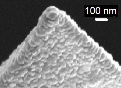

3 Experimental parameters 65 Sample 8 nm nm 5 nm 5 nm λ = 785 nm; x,.7 NA, 3 mw 3 SEM image


4 Si L-MoS /Nanocylinders heterostructure Optical image 6 nm L-MoS Intensity /cts s - 8 Micro-Raman spectra Exp E g A g Fit 9.9 cm - E g A g 53 nm, l/mm Raman shift /cm - AFM topography Intensity / cts s Au cylinders Photon energy / ev PL on MoS 53 nm Raman spectra of MoS + Si B A Wavelength / nm μm

 cm -.")


 - 785 nm, 6")
5 TERS on L-MoS /Nanocylinders heterostructure TERS (39 3) cm -.5 Intenisty / cts 8 E z 65 E E x z A g TERS enhancement, E Electric field, E x TERS spectra y LA (M) + A u E g x Si nm.5 kcts E / V m Fit 8 5 = (..) nm E Raman shift / cm - (V m V m - ) nm, 6 l/mm, 3 mw approx Milekhin et al., Nanoscale, Laterial distance / nm x k y z E 3 nm 5
 cm -.")


6 Enhancement factor and spatial resolution TERS (39 3) cm -. Milekhin et al., Nanoscale, Gauss fit to the edge + kcts 5 nm.5 Topography TERS enhancement E y k E Au λ = 785 nm R = nm EF hot spot L-MoS 6.5 X 6 (V m - ) (E / V m - ) x 6 EF = Contrast TERS = Contrast. 5 TERS 3 w = (5.3.) nm = 5. 8 nm 6 8 Au E fit R far R tip R far R hot spot Lateral distance / nm

7 Investigation of local heterogeneities Strain Peak position map Temperature rise Hot electron doping TERS (39 3) cm - 5 nm Milekhin et al., Nanoscale, kcts Normalized intensity cm - cm - / /5 / Raman shift/ cm

8 Investigation of local heterogeneities TERS (36 8) cm - E-6 nm nm E- E-3 E- V E- Topography E-5 kcts s - x cm - nm Rahaman et al., Nano Lett., (7), 7, 67 Raman shift / cm TERS intensity/ a.u Raman shift due to strain A u V E E E3 E E5 E6 cm - 3L-MoS.9 % strain Position Strain induced shift. cm - / /5 / cm Raman shift/ cm - Local heating effect.8 cm
9 Normalized intensity Raman shift / cm - Local heating due to hot spots formation Temperature dependent micro-raman study of 3L-MoS A g E g - C -5 C -5 C C 5 C 5 C 6 C C A g :. cm - /K E g :. cm - /K A g E g Fit Raman shift / cm Temperature / K Temperature rise in the hot spots =.8. 5 C 9
,6, 5836.9 % strain induced shift for A g.5 cm - Temperature induced shift for A g.8 cm -. Li et al.; ACS Nano (5),9, 58. Yu et al., Adv. Func. Mat.")
10 Quantifying hot electron doping Doping induced Raman shift = 6.7 cm - Doping gradient of phonon modes TERS intensity/ a.u. 5 5 cm - cm - / Raman shift/ cm /5 Hot electron doping of.6 3 cm - / 3 Lloyd et al.; Nano Lett. (6),6, % strain induced shift for A g.5 cm - Temperature induced shift for A g.8 cm -. Li et al.; ACS Nano (5),9, 58. Yu et al., Adv. Func. Mat. (6), 6, Najmaei et al., ACS Nano (), 8, 68 Chakraborty et al. Phys. Rev. B (), 85, 63(R) Doping gradient for A g mode =.3 3 cm - /cm -


11 Doping induced phase transition Plasmonic hot electron induced phase transition Kang et al. Adv. Mat.(),, 667
12 Doping induced phase transition Plasmonic hot electron induced phase transition 5 nm TERS (39 3) cm kcts Normalized intensity T- MoS Raman shift / cm - Milekhin et al., Nanoscale, 755 8


13 Normalized intensity Summary + 5 nm kcts Gauss fit to the edge TERS cm - EF = TERS 39 3 cm nm T- MoS.5..5 kcts 3 5 Estimated strain of.9 % and temperature rise of 5 C Plasmonic hot electron doping concentration of.6 3 cm Raman shift / cm - 3


14 Thank you for attention