CHAPTER 6 STRUCTURAL AND OPTICAL PROPERTIES OF. CdSe/CdTe MULTILAYER THIN FILMS
|
|
|
- Alexia Eaton
- 5 years ago
- Views:
Transcription
1 CHAPTER 6 STRUCTURAL AND OPTICAL PROPERTIES OF CdSe/CdTe MULTILAYER THIN FILMS
2 CHAPTER 6 STRUCTURAL AND OPTICAL PROPERTIES OF CdSe/CdTe MULTILAYER THIN FILMS 6.1 INTRODUCTION Quantum size effects in semiconductors occur when the size of the particle is small in comparison with Bohr excitonic radius which acts as a natural length scale of the electron hole pair. This effect is a direct consequence of the confined electron and hole motions in three dimensional spaces. Quantum confinement effect is characterized by discrete energy level structure and electronic transitions which have been shifted to higher energies upon decrease of the size of the particle. Qualitatively this confinement effect is similar to the problem of particle in a box. Size dependant reactivity (Beck et al. 1992), optical non linearity (Wang.Y. et al. 1987), efficient photo electron emission (Alfassi et al., 1982) and melting point reduction (Goldstein et al., 1992) are some of the interesting properties exhibited by nanoparticles. Size controlled spectral tunability adds advantage to quantum dots in the fields of optoelectronic devices, bio-labeling and photovoltaic applications (Alivisatos.A.P. 1998). The nanostructures of II-VI materials such as CdS (Potter et al. 1988), CdSe (Nesheva 1997) and CdTe (Potter.B.G. 1990) have attracted more attention for their great fundamental, experimental and applied interests. Combination of heterostructures form II-VI semiconductors promises the techniques for band engineering. Heterostructure multilayer thin films result in the formation of type I and type II band alignments (Lee.H. et al. 2009) as shown in Figure 6.1. In type I heterostructure thin films, the energy levels (valance band and conduction band) of lower band gap semiconductor 74

3 is placed in between the energy levels of higher band gap semiconductor. Whereas in type II heterostructure thin films, only valance band energy levels of lower band gap semiconductor is kept in between the energy levels of higher band gap semiconductor. The conduction band of lower band gap material is seen above the conduction band of higher band gap semiconductor. Type II heterostructure nanocrystals spatially separates photo generated carriers within the nanostructure such that the electron wave function mainly resides in one semiconductor and hole wave function in the other (Delia et al. 2004). Figure 6.1 Schematic diagrams of a) type I and b) type II heterojunction band alignment Recent investigations of type II CdSe/CdTe heterostructure nanocrystallites are ideal materials for their long range photo induced charge separation and could be applied in photovoltaic devices (Lee.H. et al. 2009; Sandeep et al. 2007; Peng et al. 2005). CdSe, CdTe and CdTe/CdSe tetrapod nanocrystals perform well in nanocrystal-polymer hybrid solar cells (Huynh et al. 2002; Sun et al. 2003; Gur et al. 2006). Few researchers have prepared type II CdSe/CdTe tetropod nanocrystals 75
4 in chemical synthesis route (Jing.W. et al. 2010; Saad et al. 2011; Kim.S. et al. 2003). In the present work, there is a formation of type II nanocrystals in CdSe/CdTe multilayer thin films prepared by physical vapour deposition method where thickness of each layer can be controlled accurately upto few nanometers. Alternate coating of CdTe and CdSe heterostructure semiconductors under high vacuum condition provides an uniform sequential arrangement of layers in the order of few nanometers so that trapping of electron-hole pair is made possible in simple steps. Crystallite sizes calculated by both Debye-Scherer formula and effective mass approximation of Brus model were smaller than the Bohr-excitonic radius. It has been generally shown that the quantum confinement effect should be observable if the radius of nano crystallites becomes less than the Bohr excitonic radius for corresponding material. 6.2 EXPERIMENTAL DETAILS CdSe/CdTe nanocrystalline multilayer thin films were prepared by consecutive thermal evaporation of CdSe and CdTe (99.99% Aldrich Chem. Co.,) from two independent molybdenum crucibles in vacuum condition at a pressure of 5x10⁻⁵ mbar. Glass substrates were used for coating thin film samples and were not intentionally heated. The nominal film thickness and deposition rate of each sub layer were controlled by calibrated digital thickness monitor (DTM). The substrates were fixed at the greatest possible distance for which the tooling factor was calculated. Step -by- step procedure was applied in the deposition of each sub layer in the multilayer structures. CdSe and CdTe single layer thin films with 50 nm thickness as reference films and three CdSe/CdTe multilayer thin film samples namely T1, T2 and T3 with different sublayer thicknesses were prepared as given in Table 6.1, to find out the changes taking place in the structural and optical properties. 76
5 Table 6.1: Details of the CdSe/CdTe multilayer thin film samples preparation S.No Name of the Sample Total Number of Layers in the sample Order of sublayers Bottom Layer Top Layer Thickness of Sublayers (Å) CdTe CdSe Total Thickness of the film (Å) 1 CdSe 1 CdSe CdTe 1 CdTe T 1 10 CdTe CdSe T 2 7 CdTe CdTe T 3 10 CdTe CdSe The structural properties of the samples were analyzed by X-Ray diffractometer (Shimadzu 6000) and Scanning Electron Microscopes (FEI Quanta FEG 200 & JEOL JSM 6390). The absorption and emission properties of the samples were studied by using UV-VIS spectrophotometer (JASCO V-550) and Photo Luminescence spectrometer (Fluorolog 3 HJY) respectively. 6.3 RESULTS AND DISCUSSION Structural Properties Structural properties of CdSe/CdTe multilayer thin films coated under specific conditions were analysed using X-ray diffraction spectra. XRD measurements allowed the identification of the nanocrystalline phases and the determination of the average crystallite sizes. The XRD profiles for the samples T1, T2 and T3 are shown in Figure 6.2. Broadness of the XRD peak indicates that the size of the crystallites is very small (Arizpe-Chávez et al., 2000). 77
6 Figure 6.2 X-Ray Diffraction Pattern of CdSe/CdTe heterostructure multilayer thin film samples T1, T2 and T3 Since the thickness of each sub layer and the size of the crystallites are in the order of few nanometers, the XRD spectra have small spike like structures throughout the range of diffraction angle. A prominent peak approximately at 24.5 o appears in all the spectra referring [JCPDS ] to (111) plane of the CdTe with cubic structure. An additional peak approximately at 25 o referring [JCPDS ] to (100) plane of CdSe with wurtzite structure is observed in the samples T1 and T3 78
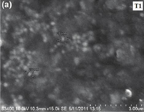
7 since CdSe was coated as top layer of few nanometer thickness intentionally on those samples. For sample T2, the peak corresponding to CdSe was concealed, as X-rays get diffracted mainly from top surface. This shows the presence of CdTe and CdSe with zincblende and wurtzite structures respectively in all CdTe/CdSe heterostructure multilayer thin films. The average sizes of nanocrystallites were determined using Scherer s expression (Klug.H.P. 1954) as given in equation 4.1. In this equation, D is the crystallite size, is the wavelength of x-ray, is the full width at half maximum (FWHM) after correcting the instrument peak broadening ( expressed in radians), and is the Bragg s angle. This method provides an estimation of the CdSe crystallite size with a maximum error of about 20 % (Arizpe-Chávez et al., 2000). Calculated size of the nanocrystallites is between 5 and 14 nm and is tabulated in Table 6.2. Table 6.2 : Size of the crystallites calculated from XRD data S.No Sample 2(deg) d(å) FWHM(deg) D (nm) 1 T T T Usually one can expect quantum size effect in this range. Surface images of CdSe/CdTe heterostructure multilayer thin film were recorded using scanning electron microscope (SEM) as shown in Figures 6.3 (a), (b) and (c). 79

8 80
, T2 (b) and T3 (c) showing distribution of the particles on the surface The particles are smoothly and uniformly distributed on")
9 Figure 6.3 Scanning Electron Microscope images of CdSe/CdTe ML samples T1 (a), T2 (b) and T3 (c) showing distribution of the particles on the surface The particles are smoothly and uniformly distributed on the surface. It is seen that the cluster of particles have formed batches on the surface of the samples. Images of HRSEM and composition ratios of CdSe and CdTe recorded using Energy Dispersive Analysis of X-rays (EDX) of sample T2 are shown in Figures 6.4 and 6.5. The layer formation in CdSe/CdTe ML thin films is seen from High Resolution Scanning Electron Microscope (HRSEM). The edges of the ML samples are scratched using micro blades to view the arrangements of CdSe and CdTe sublayers. The sublayer thickness (which is calculated from DTM) of CdSe and CdTe materials in ML sample T2 is given in Table

10 Figure 6.4 HRSEM image of sample T2 showing layer formation Figure 6.5 EDX spectra of sample T2 showing composition ratios of CdSe and CdTe 82
11 In Figure 6.5, the standard EDX spectrum recorded on ML sample T2 is given. This spectrum proves the existence of Cd, Se and Te in CdSe/CdTe ML samples. The peaks located at 3.9 and 4.2 kev confirm the presence of Tellurium characteristic lines K and L. The XPS spectrum of CdSe/CdTe ML sample T2 is shown in Figure 6.6 for further evidence for the compound formation and purity. In the XPS survey, Cd 3d peak was fitted with two components corresponding to 3d 5/2 and 3d 3/2 at and ev. The characteristic peaks at 42,573 and 583 ev confirmed the presence of Te 4d, Te 3d 5/2 and Te 3d 3/2 states. The XPS results confirmed the elemental composition of the CdSe/CdTe ML films. Figure 6.6 X- ray Photoelectron spectrum of CdSe/CdTe ML thinfilm sample T2 83
12 6.3.2 Optical properties Absorption spectra of CdSe, CdTe single layer thin films and CdSe/CdTe ML samples T1, T2 and T3 are shown in Figures 6.7 and 6.8 respectively. Figure 6.7 Absorption spectra of CdSe and CdTe single layer thin films The absorption edges of the CdSe/CdTe ML samples gradually shifted from 697 to 766 nm when the thicknesses of sublayers are changed. Since the CdSe/CdTe ML system exhibits type-ii band alignment, the possible electronic transitions may take place between valance bands of CdTe to conduction band of CdSe (Delia et al. 2004). The energy corresponding to the possible electronic transition in non quantized type II CdSe/CdTe system will be lesser than the band gaps of both the mentioned semiconductors. But these electronic transitions can be shifted to higher energies upon decrease of particle size (Pejova, 2008). 84
13 Figure 6.8 Absorption spectra of CdSe/CdTe ML samples indicating the shift of absorption edges Substructures are seen in the absorption spectra of CdSe/CdTe ML samples (Figure 6.8) but not in the spectra of CdTe and CdSe single layer thin films (Figure 6.7), which may be related to electronic transitions between discrete hole and electron energy levels in the valance and conduction bands due to spin-orbit coupling (Nesheva et al., 2002).As a result of spin-orbit interaction, valance band of CdTe semiconductor splits into an energetically higher and lower components which were usually labeled as v 7 and v 8. Transition energies between valance bands and conduction band of CdTe/CdSe ML samples T1,T2 and T3 are calculated by plotting a typical graph between energy(h) and (h) 2 as shown in Figure 6.8 by using the following relation (Tauc.J, 1979) as given in equation 4.3. Two electronic transitions were observed in Figures 6.9 (a), (b) and (c) rather than obtaining a single transition as in bulk CdSe and CdTe material. The transitions close to the fundamental band gap (E g ) of II-VI semiconductors arise due to the spin-orbit split 85
14 of valance band energy levels (Baldereschi et al. 1971). Based on the model proposed by Chestnoy et.al (1986), the valance band components v 7 and v 8 are split into discrete hole states as depicted in Figure 5.9. This proposed model has made the task of assigning the electronic transitions with the energy values quiet straightforward. 86
15 Figure 6.9 The plots of (h) 2 versus (h) graph for the samples T1(a), T2(b) and T3(c) with 7 v 6 c and 8 v 6 c transitions 87
16 According to the energy order, the obtained energy values in sample T1 (1.78 and 1.98eV), T2 (1.7 and 1.88 ev) and in T3 (1.62 and 1.8 ev) given in Figures 6.9 (a), (b) and (c) may be attributed to the transitions taking place between 1S-1S and 1S - 1S energy states respectively (Pejova et al. 2005; Woggon et al. 1996). The calculated band gap energies (E g ) as given in Table 6.3 are higher than the band gap of bulk CdTe (E g(bulk) ) ie., 1.54 ev at room temperature (Sharma et al., 2005). As it can be seen from Table 6.3, the confinement energies (E-E g(bulk) ) for the samples T1, T2 and T3 are large which states that the prepared ML samples are strongly quantized (Pejova et al. 2005). Size of the particles can be calculated from the band gap shift (E g - E g(bulk) ) with respect to bulk band gap value of CdTe using Brus effective mass approximation equation as given in equations 4.4 where E g is the band gap values obtained from experiment, E g(bulk) is the band gap of bulk CdTe (= 1.54 ev), d is the diameter of the crystallites and (= m e ) is the effective mass of electron-hole pair as given by equation 4.5. The bulk energy gap value of lesser band gap material should be considered in energy shift calculation for heterostructured materials. It has been generally considered that the quantum confinement effect should be observable if the radius of nanocrystallites becomes less than the Bohr excitonic radius of the corresponding material. The bulk Bohr diameter of the Wannier exciton in CdTe is 14 nm (Sharma et al., 2005). The average size of the nanocrystallites calculated using equation (4.4) varies between 7 to 12 nm as tabulated in Table
17 Table 6.3: Size of the crystallites from UV Vis data by Brus model S. No Sample E( 7 v - 6 c ) ev E g ( 8 v - 6 c ) ev (E- E g(bulk) ) ev (E- E g(bulk) ) ev Shift in Band Gap (E g - E g(bulk) ) ev D (nm) 1 T T T It is evident that the nanocrystallite sizes (D o ) of the CdTe/CdSe heterostructure multilayer thin film samples are much smaller than the Bohr exciton diameter (D B ). If D o /D B <<2, the crystal exhibits a single particle confinement behavior in which electrons and holes are independently confined. Hence, the prepared CdTe/CdSe heterostructure multilayer thin films show the quantum confinement effect. Size of the crystallites calculated from effective mass approximation is not precisely matching with the size of the crystallites calculated from X-ray diffraction spectra. In order to explain the observed discrepancy one should take into account that the full width at half maximum of X-ray diffraction peaks depends not only on the nanocrystal size but also on existing microstrains and deformations in the nanocrystal arrangement (Suchitra Sen et al. 1974). The emission spectra recorded for CdSe/CdTe heterostructure multilayer thin film samples T1, T2 and T3 are shown in Figure The emission peaks of CdTe/CdSe samples are observed at longer wavelengths than that of the individual layers as it is the characteristic feature of type II quantum dots. It is found that the intensity of emission peak and smoothness increase when the particle size increases. Moreover, the emissions of the CdSe/CdTe heterostructure samples are more structured than the individual CdSe and CdTe bands. There is a splitting of the emission maximum observed with the bands centered on 410 nm and 435 nm in ML samples. This might be due to the presence of CdSe and CdTe individual peaks appearing together with shifting at longer wavelength side. In this type of 89
18 heterostructure multilayer thin films, the energy of the emission thus depends on the band offsets of the two materials (lesser band gap and higher band gap) and can emit at energies smaller than the band gap of either material (Kim et al. 2003). Figure 6.10 Photoluminescence Spectra of CdSe/CdTe ML samples T1, T2 and T3 along with CdSe and CdTe single layers 90
19 The FWHM of the ML samples is another noteworthy entity. FWHM of CdSe/CdTe ML samples are larger than 40 nm, which is far larger than that of ordinary bulk semiconductor sample. The main reason of this phenomenon is the size fluctuation of the quantum dots (Mao et al., 2005). The FWHM of the CdSe/CdTe ML sample T1 is the largest, because the size of the particle in this sample is smallest and the quantum confinement effect is most notable. The large stokes shift between the absorption maximum and the PL band may be due to the presence of at least one deep trapping site and electron hole recombination via trap state (Chaure.S. et al. 2005). 6.4 CONCLUSION CdSe/CdTe multilayer thin films with various sublayer thicknesses were prepared using physical vapor deposition technique. Sequential thermal evaporation technique is made possible to adjust the layer thickness precisely. This method gives the possibility of preparing nanocrystals of various semiconductors with a relatively smaller size distribution than the conventional method. Quantum confinement effect is explained in connection with structural and optical properties of CdSe/CdTe ML systems. XRD studies are used to calculate average size of the crystallites using the peaks corresponding to (111) and (100) planes of CdTe and CdSe respectively. Bulk CdTe has band gap energy of 1.54eV that can be shifted to larger values by reducing the crystallite size to dimensions smaller than the Bohr radius of the exciton. Experimentally measured energy levels show the spin-orbit split of valance band of CdTe. Spin-orbit split of valance band of CdTe has been discussed from (h) 2 versus (h) graph and absorption spectra. Crystallite sizes (7-12 nm) are determined with the predictions of effective mass approximation model (i.e., Brus model) which shows that the diameter of crystallites is smaller than the Bohr exciton diameter (14 nm) of CdTe. It is found that the emission peaks of the prepared CdSe/CdTe ML samples were shifted from the peaks of CdSe and CdTe single layers towards red region as a characteristic feature of type II band alignment 91
20 and FWHM is a size dependent quantity which changes with change of the particle size. It is concluded that the sublayer thickness in ML systems is one of the factors which plays an important role in quantum confinement effect. 92