Materials Science and Engineering
|
|
|
- Dwain Stephens
- 5 years ago
- Views:
Transcription
1 Introduction to Materials Science and Engineering Chap. 3. The Structures of Crystalline Solids How do atoms assemble into solid structures? How does the density of a material depend on its structure? When do material properties vary with the sample (i.e., orientation)? 1
2 Content 1 Introduction 2 Unit Cell 3 Crystal Structure 4 Crystallographic Directions and Planes 5 Interstitial Position & Coordination Number 6 Structure Determination (X-Ray Diffraction) 2
3 Introduction In chapter 2, you have learned the various types of atomic bonding. In chapter 3, we will learn the atomic arrangements in the solid state. Solid materials are classified according to the regularity with which atoms and ions are arranged with respect to one another. 3 Solid So, Materials how are : they arranged? Solid Materials a) Periodically having a long range order in 3-D: Crystalline b) Randomly having a short range order with the characteristics of bonding type, but losing the long range order: Amorphous
4 Introduction Materials and Packing 1. Crystalline materials Atoms pack in periodic, 3D arrays. Typical of - metals - many ceramics - some polymers 2. Noncrystalline materials... Atoms have no periodic packing. Occurs for - complex structures -rapid cooling Amorphous = Noncrystalline Si crystalline SiO2 Oxygen 4 noncrystalline SiO2
5 Introduction The arrangement of atoms in a material influence its physical and mechanical behavior: - Remember that most of the properties of materials result from the bonding nature of atoms in solids, not the properties of atoms by itself. Al provides good ductility. Fe provides good strength. Polyethylene is easily deformed. Rubber can be elastically stretched. 5
6 Content 1 Introduction 2 Unit Cell 3 Crystal Structure 4 Crystallographic Directions and Planes 5 Interstitial Position & Coordination Number 6 Structure Determination (X-Ray) 6
7 Lattice Unit cell 3D point array in space, such that t each point has identical surroundings. These points may or may not coincide with atom positions. example: iron (Fe) -- body centered cubic (Fig. 3-2) 7


8 Unit cell Unit cell Smallest repetitive volume which contains the complete lattice pattern of a crystal. 8
9 Unit cell Unit cell 9
10 Unit cell Lattice parameters length: a, b, c angle: α, β, γ 10
11 Unit cell 7 crystal systems (Table 3-2) 11
12 Unit cell 7 crystal systems (continued) (Table 3-2) 12


13 Unit cell 14 Bravais Lattice - Only 14 different types of unit cells are required to describe all lattices using symmetry cubic hexagonal rhombohedral (trigonal) tetragonal orthorhombic monoclinic triclinic P I F 13 C
14 Content 1 Introduction 2 Unit Cell 3 Crystal Structure 4 Crystallographic Directions, and Planes 5 Interstitial Position & Coordination Number 6 Structure Determination (X-Ray) 14
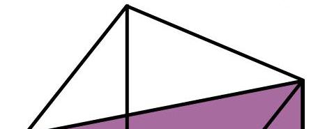
15 Crystal system Hard Sphere model is used to describe crystalline structures. t s (Fig. 3-1) face-centered cubic (FCC) 15
16 Crystal system Tend to be densely packed. Have several reasons for dense packing: Typically, several elements are present, and each atomic radius is the same. Metallic bonding is not directional. Nearest neighbor distances tend to be small, for lower bond energy. Have the simplest crystal structures. 16
17 Crystal system Simple Cubic Structure t (SC) Rare due to low packing density Only Po (polonium) has this structure. Close-packed directions are cube edges Coordination # = 6 (# of nearest neighbors) 1 atom/unit cell: 8 corners X 1/8 17 (Courtesy P.M. Anderson)
18 Crystal system Atomic Packing Factor (APF) Volume of atoms in unit cell* APF = Volume of unit cell (Eq. 3-2) *assume hard spheres APF for a simple cubic structure = 0.52 a R=0.5a close-packed directions atoms / unit cell volume / atom π (0.5a)3 APF = a 3 volume / unit cell 18 contains 8 x 1/8 = 1 atom / unit cell
, Ta, Mo Coordination # = 8 (# of nearest neighbors) 2 atoms/unit cell: 1 center + 8 corners X 1/8 (Fig. 3-2) 19 (Courtesy P.M. Anderson)")
19 Crystal system Body Centered Cubic Structure t (BCC) Atoms touch each other along cube diagonals Close packed directions are cube diagonals <111> Highest density plane {110} ex: Cr, W, Fe (α), Ta, Mo Coordination # = 8 (# of nearest neighbors) 2 atoms/unit cell: 1 center + 8 corners X 1/8 (Fig. 3-2) 19 (Courtesy P.M. Anderson)
20 Crystal system APF of BCC structure = a a 2 a Close-packed directions: R length = 4R = a 3 a 20 atoms / unit cell APF = π ( 3a/4)3 a 3 volume / atom volume / unit cell
 4 atoms/unit cell: 6 face X 1/2 + 8 corners X 1/8 (Fig. 3-1) 21 (Courtesy P.M.")
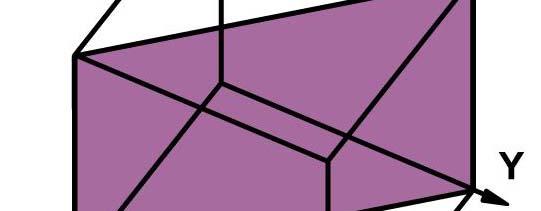
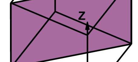
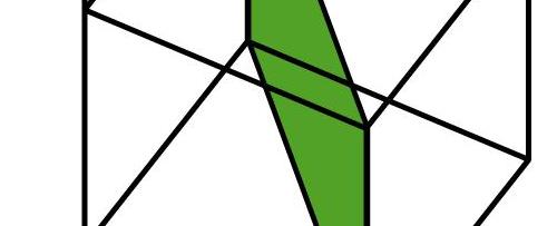
21 Crystal system Face Centered Cubic Structure (FCC) Atoms touch each other along face diagonals Close packed directions are edge diagonals <110> Highest density plane {111} ex: Al, Cu, Au, Pb, Ni, Pt, Ag Coordination # = 12 (# of nearest neighbors) 4 atoms/unit cell: 6 face X 1/2 + 8 corners X 1/8 (Fig. 3-1) 21 (Courtesy P.M. Anderson)
22 Crystal system APF of FCC structure = 0.74 Close-packed directions: length = 4R = 2 a a atoms / unit cell APF = π ( 2a/4)3 a 3 volume / atom volume / unit cell
 ex: Cd, Mg, Ti, Zn Coordination # = 12 (# of")
 a / c = 1.633 APF = 0.74 (Fig.")
23 Crystal system Hexagonal Closed Packing Structure (HCP) ex: Cd, Mg, Ti, Zn Coordination # = 12 (# of nearest neighbors) 2 atoms / unit cell (1 + 4 x 1/6 + 4 x 1/12) a / c = APF = 0.74 (Fig. 3-3) 23 Unit cell
 (Fig.")
24 Crystal system Hexagonal Closed Packing Structure (HCP) (Fig. 3-3) 24

25 Crystal system 25
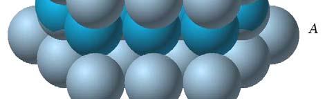
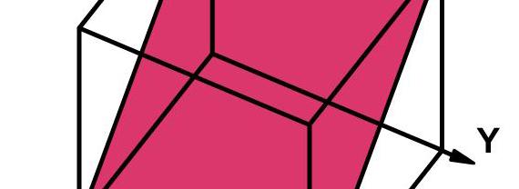
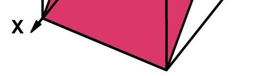
26 Crystal system Close Packing Crystal structure How can we stack metal atoms to minimize empty space? close packed atomic arrangement in 2-D Now stack these 2-D layers to make 3-D structures 26
 (Fig. 3-14) (Fig. 3-15) 27")
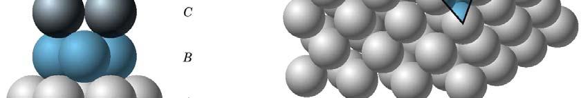
27 Crystal system Stacking sequence A A A A A B B B B C C C C A A A A A B B B B C C C C A A A A A B B B B C C C C A A A A A B B B B C C C C A A A A A (Fig. 3-13) (Fig. 3-14) (Fig. 3-15) 27

 (Fig.")
28 FCC A B C A B C stacking sequence FCC A A A A A B B B B C C A A A C C A A B B B B C C C C A A A A A B B B B C C C C A A A A A B B B B C C C C A A A A A (Fig. 3-13) (Fig. 3-15) B A C B A C B A 28


 (Fig.")
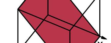
29 HCP A B A B A B stacking sequence HCP A A A A A B B B B C C C C A A A A A B B B B C C C C A A A A A B B B B C C C C A A A A A B B B B C C C C A A A A A ? 29 (Fig. 3-14) (Fig. 3-15) A B A B A B A


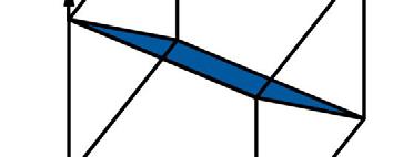
30 Crystal system FCC vs. HCP HCP FCC 30 Both have the same APF.
31 Crystal system Density Density = ρ = Mass of Atomsin UnitCell TotalVolume ofunitcell n A ρ = (Eq. 3-5) V C N A where n = number of atoms/unit cell A = atomic weight (g/mol) V C = Volume of unit cell = a 3 for cubic (cm 3 /unit cell) N Avogadro s A = number = x (atoms/mol) 31
32 Crystal system Density Example Copper (from Periodic Table) Crystal structure = FCC: 4 atoms/unit cell Atomic weight = g/mol (1 amu = 1 g/mol) Lattice constant a = nm (1 nm = 10-9 m) ρ(cu) = 8.97 g/cm 3 32
33 Crystal system Density Example - Cr (BCC) A = g/mol R = nm n = 2 a = nm R a ρ = 7.19 g/cm 3 ρ = a x
34 Crystal system Densities of Material Classes ρ(metals) > ρ(ceramics) > ρ(polymers) 34 Why? Metals have... close-packing (metallic bonding) large atomic mass Ceramics have... less dense packing often lighter elements Polymers have... ρ(g/ /cm 3 ) poor packing (often amorphous) 1 lighter elements (C, H, O) Composites have... intermediate values Metals/ Alloys Platinum Gold, W Tantalum Silver, Mo Cu,Ni Steels Tin, Zinc Titanium Aluminum Magnesium Graphite/ Ceramics/ Semicond Polymers Composites/ Fibers *GFRE, CFRE, & AFRE are Glass, Carbon, & Aramid Fiber-Reinforced Epoxy composites (values based on 60% volume fraction of aligned fibers in an epoxy matrix). Zirconia Al oxide Diamond Si nitride Glass -soda Concrete Silicon Graphite PTFE Data from Table B1, Callister 7e. Silicone PVC PET PC HDPE, PS PP, LDPE Glass fibers GFRE* Carbon fibers CFRE * Aramid fibers AFRE * Wood
35 Content 1 Introduction 2 Unit Cell 3 Crystal Structure 4 Crystallographic Directions and Planes 5 Interstitial Position & Coordination Number 6 Structure Determination (X-Ray) 35


 P: q, r, s (Fig.")
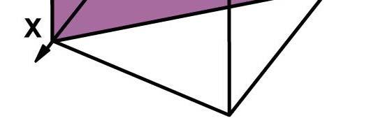
36 Crystallographic Directions and Planes Crystallographic Coordinates Position: fractional multiples of unit cell edge lengths ex) P: q, r, s (Fig. 3-5) 36
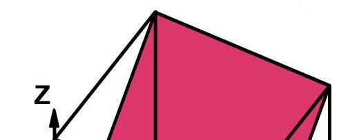
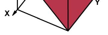
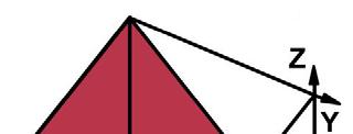
37 Crystallographic Directions and Planes Crystallographic Directions: a line between two points or a vector [uvw] square bracket, smallest integer families of directions: <uvw> angle bracket A (Fig. 3-6) 37
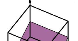
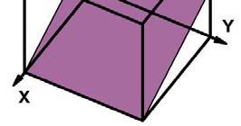
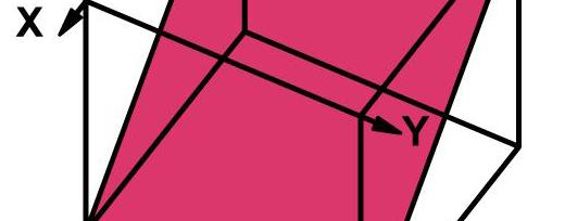
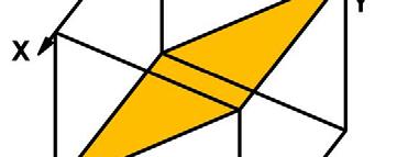
38 Crystallographic Directions and Planes Crystallographic Planes (hkl): p Miller Indices: Reciprocals of the three ur axial intercepts for a plane, cleared of c fractions & common multiples. All parallel ur ur a b n y planes have the same Miller indices h k l (hkl) m n p x m z Algorithm 1. Read off intercepts of plane with axes in terms of a, b, & c. 2. Take reciprocals of intercepts. 3. Reduce to smallest integer values. 4. Enclose in parentheses, no commas i.e., 38 (hkl). Example 1. let m = 2, n = 1, p = 2. reciprocals are 1/2, 1, 0 3. then, h = 1, k = 2, l = 0 4. Miller index is (120)
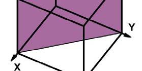

39 Crystallographic Directions and Planes Crystallographic Planes (Fig. 3-9) A B C D E F
40 Crystallographic Directions and Planes Crystallographic Planes (Fig. 3-9) 40

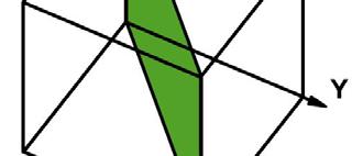

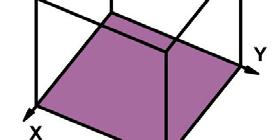
41 Crystallographic Directions and Planes Crystallographic Planes Family: ex. {110} 41
42 Crystallographic Directions and Planes Crystallographic Planes Family: ex. {110} 42

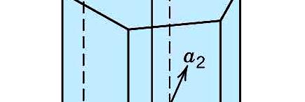
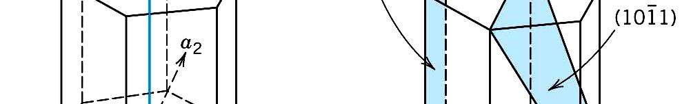
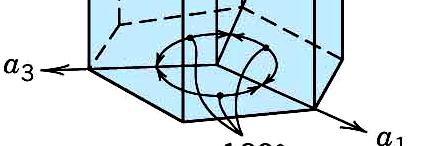
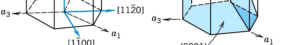
43 Crystallographic Directions and Planes Hexagonal Crystal System Miller-Bravais Scheme (skip) 43 [ uvtw ] ( hkil ) t = ( u+ v) i = ( h+ k)
44 Crystallographic Directions and Planes Directions, Planes, and Family Line and direction [111] square bracket <111> angular bracket - family Plane (111) round bracket (Parentheses) {111} braces - family 44


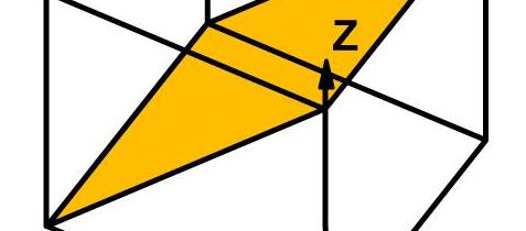
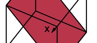
45 Crystallographic Directions and Planes Linear & Planar Density number of atoms centered on direction vector LD= length of direction vector number of atoms centered on a plane PD= area of plane 2 atoms 1 2 atoms 1 ex) LD = 110 PD = = = (Fig. 3-10) 4R 2R 8 2R 4 2R 45 Slip occurs on the most densely packed crystallographic planes, along directions having the greatest atomic packing in those planes
 46")
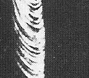
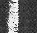
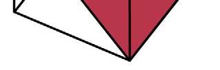
46 Slip (Fig. 7-9) 46 Plastically stretched zinc single crystal
47 Content 1 Introduction 2 Unit Cell 3 Crystal Structure 4 Crystallographic Directions, and Planes 5 Interstitial Position & Coordination Number 6 Structure Determination (X-Ray) 47
48 Interstitial Position & Coordination Number Interstitial sites in FCC 48 Octahedral sites Tetrahedral sites
49 Content 1 Introduction 2 Unit Cell 3 Crystal Structure 4 Crystallographic Directions, and Planes 5 Interstitial Position & Coordination Number 6 Structure Determination (X-Ray Diffraction) 49


 (Fig.")


50 Crystals as Building Blocks Some engineering applications require single crystals: - diamond single-crystal powders for abrasives - turbine blades (Fig. 8-33) (Fig. 3-16) 50 Crystal properties reveal features of atomic structures. Ex: Certain crystal planes in quartz fracture more easily than others.
51 Polycrystals Most engineering materials are polycrystals 1 mm Nb-Hf-W plate with an electron beam weld Each "grain" is a single crystal. If crystals are randomly oriented, overall properties are not directional. 51


52 Crystalline nature of materials - Grains A grain is a region of distinct crystal orientation within a polycrystalline material. The grain boundary is the interface between individual grains. Grain boundaries have significant influences on the properties of the material. 52 Silicon iron alloy Oxford instrument
53 Various stages in the solidification of a polycrystalline p y y material (Fig 3-17) (Fig. 3 17) Grain boundary Grain 53
54 Structure Determination (X-Ray) Diffraction of Light Young s experiment 54
55 Structure Determination (X-Ray) Diffraction The scattering centers (atoms), have spacing comparable in magnitude to the wavelength. Diffraction results from specific phase relationships established among the waves scattered by the scattering atoms (centers). 55
56 Structure Determination (X-Ray) Electromagnetic wave 56
 X-ray Diffraction")


57 Structure Determination (X-Ray) X-ray Diffraction Detector X-ray source Specimen X-ray source Detector Goniometer 2d sinθ = nλ hkl hkl Al powder (Fig. 3-21) 57
58 Structure Determination (X-Ray) Bragg s Law AB+BC = 2dsinθ = nλ O A B C 58 Interplanar spacing (Fig. 3-19) a d hkl = (in cubic) h+k+l
59 Structure Determination (X-Ray) Determination of Crystal Structures Problem: Determine the d-spacing for the (111) plane, the lattice parameter a 0 and the atomic radius for Al. 59 o 2 θ = 38 θ = λ d 19 o for ( 111) λ nm = 2 d sin θ d 111 = = = o 2 sin θ 2 sin 19 hkl = h 2 a o + k 2 + l ( ) nm 2 a o = d hkl h 2 + k a o = x nm = x 3 nm 4 r a o 2 a o = nm; a o = r = = nm l 2
60 Structure Determination (X-Ray) Indexing example: polycrystalline p y y α-iron (BCC) z c z y c a b x a b x y a x z c b y 60
")
61 Scanning Tunneling Microscopy (STM) 61
62 Scanning Tunneling Microscopy Silicon (001) Surface 62
![The Si(001)-(2 1) Reconstruction [010] [110] Unreconstructed Si(001)-(1 1) surface.](/docs-images/88/116845820/images/63-2.jpg "The Si atoms of the topmost layer are highlighted in orange.")
-(2 1) ( ) surface.")
63 The Si(001)-(2 1) Reconstruction [010] [110] Unreconstructed Si(001)-(1 1) surface. The Si atoms of the topmost layer are highlighted in orange. These atoms are bonded only two other Si atoms, both of which are in the second layer (shaded grey). [010] [110] Reconstructed Si(001)-(2 1) ( ) surface. The Si atoms of the topmost layer form a covalent bond with an adjacent surface atom are thus drawn together as pairs. Z. Zhang et al. (Oak Ridge National Laboratory) Annual. Rev. Mater. Sci. 27, 525 (1997) 63


64 Scanning Tunneling Microscopy Atoms can be arranged and imaged: 64 Carbon monoxide molecules arranged on a platinum (111) surface. Iron atoms arranged on a copper (111) surface.
65 Summary Atoms may assemble into crystalline or amorphous structures. We can predict the density of a material, provided we know the atomic weight, lattice constant, and crystal geometry (e.g., FCC, BCC, or HCP). Material properties generally vary with the single-crystal orientation (i.e., they are anisotropic). In polycrystals with randomly-oriented grains, properties are generally non-directional (i.e., they are isotropic) Problems from Chap. 3 Prob. 3-1 Prob. 3-4 Prof. 3-8 Prob Prob Prob Prob Prob Prob Prob Prob Prob Prob. 3-60(a) Prob Prob. 3-66