3. Solidification & Crystalline Imperfections
|
|
|
- Regina Hall
- 5 years ago
- Views:
Transcription
 formation of a grain structure formation of stable nuclei two main mechanisms a.")
1 3. Solidification & Crystalline Imperfections solidification (casting process) of metals divided into two steps (1) nucleation formation of stable nuclei in the melt (2) growth of nuclei into crystals (3) formation of a grain structure formation of stable nuclei two main mechanisms a. homogeneous nucleation liquid metal is cooled below freezing point, slow-moving atoms bond together to create homogeneous nuclei nucleus larger than critical size, can grow into a crystal embryo smaller than critical size, continuously being formed and redissolved in the molten metal 1
2 two kinds of energies involved in homogeneous nucleation: (1) the volume free energy ΔG V free energy difference between the liquid and solid ΔG V = 4/3πr 3 ΔG v (2) the surface energy ΔG s the energy needed to create a surface for the spherical particles ΔG s = 4πr 2 γ γ: specific surface free energy of the particle total free energy ΔG T = ΔG V + ΔG s ΔG T = 4/3πr 3 ΔG v + 4πr 2 γ r* : critical radius ΔG T reaches the maximum 2
3 d(δg T )/dr = 0 when r = r* 2γ r* = - ΔGv critical radius versus undercooling critical nucleus size mainly determined by ΔG V amount of undercooling increases, the critical nucleus size decreases the relationship is 2γT m r* = ΔH f ΔT γ: surface free energy T m : freezing temperature ΔH f : latent heat of fusion ΔT: amount of undercooling 3
4 ex. calculate the critical radius of homogeneous nucleus forms from pure liquid Cu. Assume ΔT = 0.2ΔT m (γ = J/cm 2, T m = 1083 o C, ΔH f = 1826 J/cm 3 ) calculate the number of atoms in criticalsized nucleus at this undercooling ΔT = 0.2ΔT m = 1356 K 0.2 = 271 K 2γT m 2( J/cm 2 )(1356 K ) r* = = ΔH f ΔT (1826 J/cm 3 )(271 K) = cm volume of nucleus = 4/3 π ( cm) 3 = cm 3 Cu: FCC structure, unit length a = cm 4 atoms per unit cell volume of unit cell = ( cm) 3 = cm cm 3 number of atoms = 4 = 325 atoms cm 3 b. heterogeneous nucleation occurs in a liquid on the surface of its container, insoluble impurities and other structural materials that lower the critical free energy required to form a stable nucleus 4
")
5 the surface energy to form a stable nucleus on the nucleating agent is lower much smaller amount of undercooling is required to form a stable nucleus crystal growth and grain formation nuclei crystals grains polycrystalline solidified metal containing many crystals grains crystals in solidified metal grain boundaries the surfaces between the grains two major types of grain structures: (1) equiaxed grains crystals grow about equally in all directions, commonly found adjacent to a cold mold wall (2) columnar grains long, thin, coarse grains, created when metal solidifies 5

6 rather slow in the presence of a steep temperature gradient columnar grains grow perpendicular to the mold surface Al ingot solidification of single crystals solidification takes place around a single nucleus, no other crystals are nucleated and grow the interface temperature between solid and liquid must be slightly lower than m.p. of solid and the liquid temperature must increase beyond the interface 6
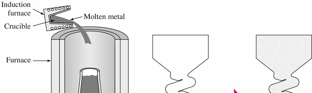
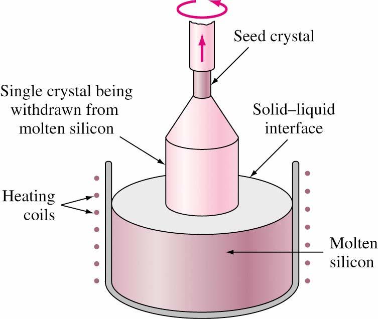
7 single-crystal gas turbine airfoil Si single crystal Czochralski method 7

8 metallic solid solution metal alloy mixture of two or more metals or a metal (metals) and a nonmetal (nonmetals) ex. cartridge brass: 70% Cu + 30% Zn Ni-base superalloy Inconel 718: about 10 elements in its nominal composition solid solution solid that consists o two or more elements atomically dispersed in a singlephase structure (1) substitutional solid solution solute atoms can substitute for parent solvent atoms in a crystal lattice ex. (111) plane in an FCC crystal lattice Hume-Rothery rules: the following conditions are favorable for extensive solid solubility of 8 one element in another:
9 (a) the diameters of the atoms of the elements must not differ by more than about 15% (b) the crystal structures of the two elements must be the same (c) no appreciable difference in the electronegativites of the two elements (d) two elements should have the same valence ex. Using the following data, predict the relative degree of atomic solid solubility of the elements in copper atomic radius crystal structure electro- negativity valence Cu nm FCC Zn nm HCP Pb nm FCC , +4 Si nm diamond cubic Ni nm FCC Al nm FCC Be nm HCP Cu-Zn Cu-Pb Cu-Si Cu-Ni Cu-Al Cu-Be Δr +3.9% +36.7% -8.6% -2.3% +11.7% -10.9% Δχ predict B E C A C C solubility exp. 38.3% 0.1% 11.2% 100% 19.6% 16.4% 9

 2 R")
10 (2) interstitial solid solution the solute atoms fit into the spaces between the solvent atoms, the spaces are called interstices interstitial solid solution can form when one atom is much larger than another C in γ-fe max. 2.08% C can dissolve ex. calculate the radius of the largest interstitial void in FCC γ-fe lattice 2R + 2r = a 2R = 2(R + r) 2 R = R + r r = ( 2-1) R = R = nm = nm 10

11 crystalline imperfection zero-dimensional or point defects one-dimensional or line defects (dislocation) two-dimensional or planar defects three-dimensional or volume defects (1) point defects vacancy atom is missing, may be created by local disturbances during the crystal growth atomic arrangements in an existing crystal plastic defromation, rapid cooling bombardment with energetic particles interstitialcy or self-interstitial an atom in a crystal can occupy an interstitial site between surrounding atoms can be introduced by irradiation 11
 line defects (dislocations)")
12 Schottky imperfection two oppositely charged ions are missing form an ionic crystal a cation-anion divacancy Frenkel imperfection a cation moves into an interstitial site, and a cation vacancy is created vacancy-interstitialcy pair the presence of these defects in ionic crystals increases their electrical conductivity impurity is also a type of point defect (2) line defects (dislocations) crystalline solids are defects that cause lattice distortion centered around a line formed by plastic deformation, vacancy condensation, and atomic mismatch 12


13 two types of dislocations a. edge dislocation created by the insertion of an extra half plane of atoms above slip or Burgers vector displacement distance of atoms around the dislocation and is perpendicular to the edgedislocation line region of compressive strain where the extra half plane is, region of tensile strain below the extra half plane 13

14 b. screw dislocation formed by applying upward and downward shear stress to a perfect crystal that have been separated by a cutting plane the slip vector is parallel to the dislocation line most dislocations are of the mixed type 14

15 (3) planar defects external surface the most common type of planar defect, the atoms on the surface are bonded to other atoms only on one side, the higher energy associated with these atoms makes the surface susceptible to reaction grain boundaries a narrow region between two grains of about 2~5 atomic diameters in width and a region of atomic mismatch between adjacent grains the higher energy of grain boundaries and more open structure make them more favorable for nucleation and growth of precipitates 15

16 twin or twin boundary a region in which a mirror image of the structure exists across a plane or a boundary ex. twin boundaries in the grain structure of brass small-angle tilt boundary small-angle twist boundary misorientation angle θ is generally < 10 o small-angle boundaries are regions of high energy and tend to strengthen a metal 16
17 stacking faults or piling-up faults one or more of the stacking planes may be missing, give rise to another twodimensional defect ex. ABCABAACBABC in FCC crystal ABAABBAB in HCP crystal (4) volume defects a cluster of point defects join to form a three-dimensional void or a pore a cluster of impurity atoms join to form a three-dimensional precipitate the size from a few nm to cm 17
18 identification of microstructure and defects (1) optical metallography technology at the μm level (magnification 2000 ) information about grain size, grain boundary, existence of various phases, internal damage, defects may be extracted sample preparation: i grinding stage ii polishing stage smooth, mirror-like surface must be produced after polishing stage iii etching process the atoms at the grain boundary will be attacked at a much more rapid rate than the atoms inside the grain tiny groves along the boundaries are produced grain size and average grain diameter American Society for Testing and Materials (ASTM) method N = 2 n-1 n : grain-size number n < 3 : coarse-grain, 4 < n < 6 : medium-grain 7 < n < 9 : fine-grain n > 9 : ultra-large grain 18
19 average grain diameter d = C/(n L M) C = 1.5 constant M : magnification n L : the ratio of the number of grains intersected by a line of known length schematic diagram of optical microscope 19


20 microstructure observed in optical microscope low-carbon steel magnesium oxide (magnification 100 ) (magnification 225 ) ex. 64 grains/in 2 in a photomicrogarph of a metal are observed at a magnification of 100. What is the ASTM grain size number? N = 2 n-1 64 = 2 n-1 n = 7 20


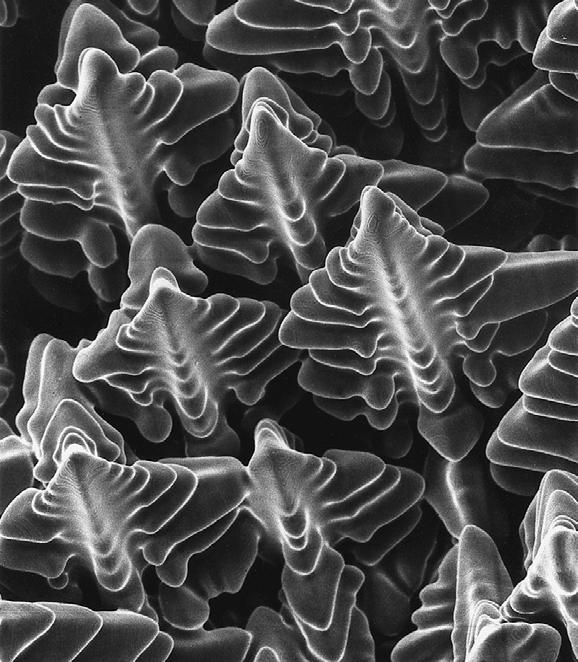
21 (2) scanning electron microscopy (SEM) used for microscopic feature measurement, fracture characterization, microstructrue studies, thin coating evaluation, surface contamination examination, failure analysis wide range of magnification 15 ~ 100,000 resolution to about 5 nm easy to prepare sample, often coated with Au SEM of intergranular corrosion fracture 21

22 schematic diagram of SEM 22
 in materials resolved features in the")

23 (3) transmission electron microscopy (TEM) important technique for studying defects and precipitates (secondary phase) in materials resolved features in the nm range samples have a thickness of several hundred nm and sample preparation is complex bright-field image the direct electrons dark-field image the scattered electrons 23

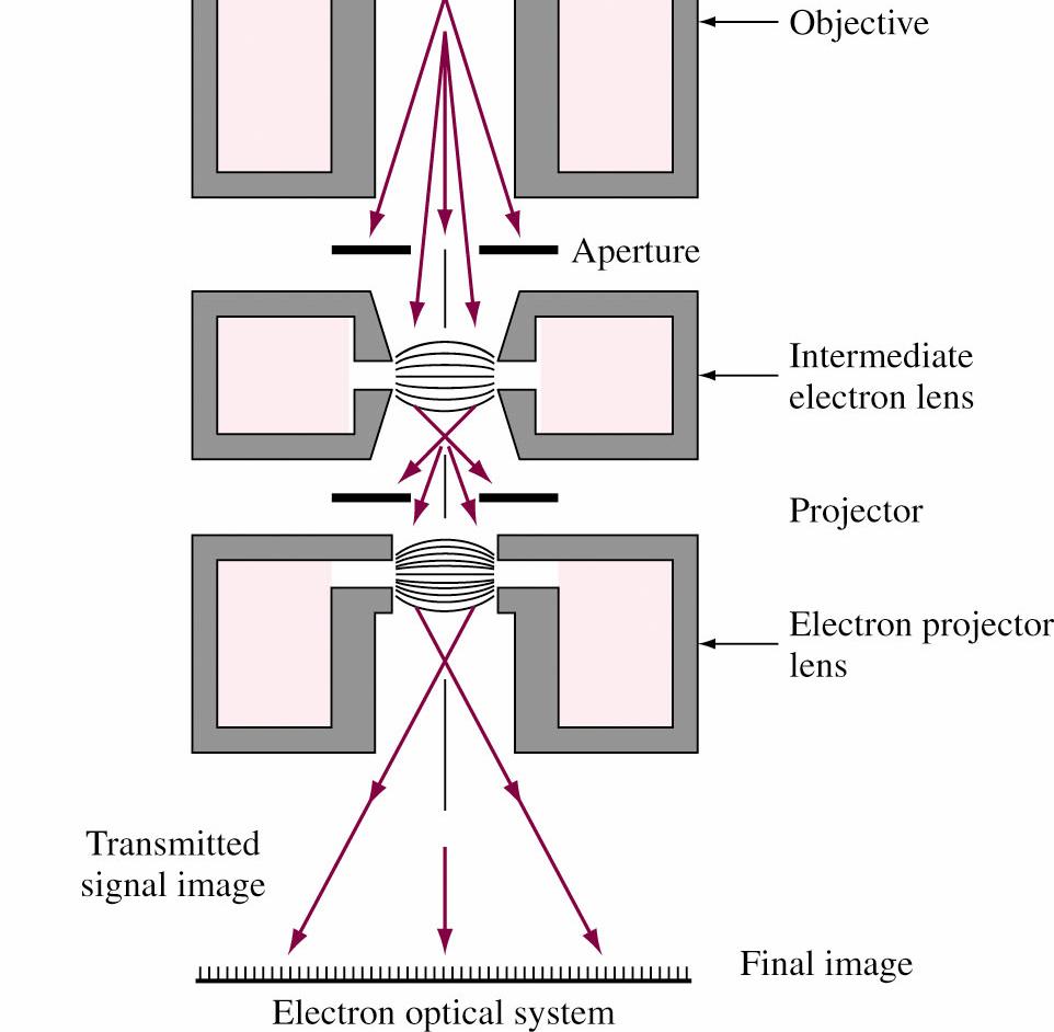
24 schematic diagram of TEM 24

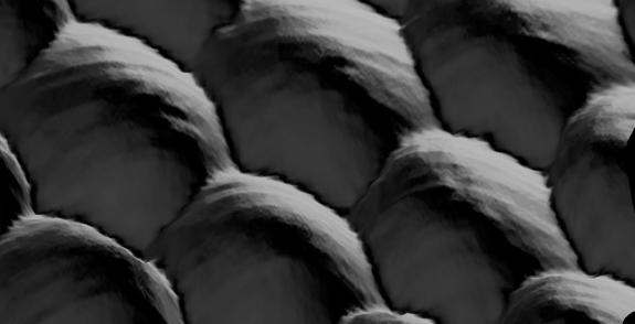
25 (4) high-resolution transmission electron microscopy (HRTEM) has a resolution of about 0.1 nm allowing viewing of crystal structure and defects at the atomic level sample must be significantly thin 10 ~ 15 nm HRTEM image of several dislocations forming a small-angle boundary 25


26 (5) scanning probe microscopes (SPM) tools allow scientist to analyze and image materials at the atomic level (a) scanning tunneling microscope (STM) invented by Binnig and Rohrer in early 1980s extremely sharp tip (made of W, Ni, Pt-Ir, Au, or carbon nanotube) to probe the surface constant current mode constant height mode 26
27 (b) atomic force microscope (AFM) contact mode short-range repulsive force noncontact mode long-range attractive force AFM can be applied to all materials even nonconductor 27
28 28