Notable Trends in CMP: Past, Present and Future
|
|
|
- Muriel Wilkinson
- 5 years ago
- Views:
Transcription


1 Notable Trends in CMP: Past, Present and Future Semiconductor International February 15 th, 2007 Pete Singer Editor-in-Chief Levitronix CMP Users Conference 2007


2 April 1988: Etchback, SOG


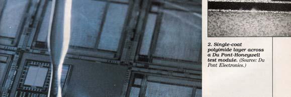
3 November 1990: SOG, Etchback, CMP


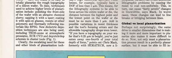
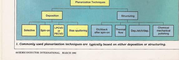
4 March 1992: Local vs Global


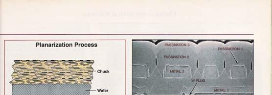
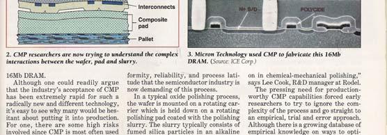
5 February 1994: Pads and Slurries


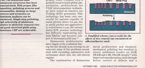
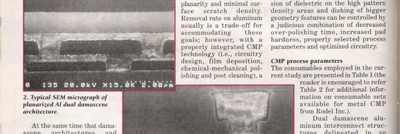

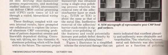
6 October 1995: Dual Damascene Al

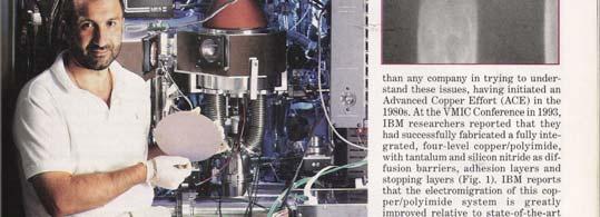
7 November 1994: Cu and Low k

8 Albany Nanotech Today

9 November 1995: Maturation

10 0.8 Advanced Electronic Materials Film Characteristics Fracture/Mechanical Toughness Physical/Electrical Film Character Integrat -ion F Toughness, MPa-m^1/ Oxide SiLK* Dielectric Constant Empirical data indicates fracture toughness below 0.3 MPa-m^1/2 is problematic for CMP stacks and back-end packaging (wire bonding) * Trademark of The Dow Chemical Company
11 2002: Endpoint enhances Copper CMP Process Control Stages of Copper polish: (for edge thin Cu deposition or edge-fast Cu CMP removal) Pre-CMP Topography: Copper Planarized Edge clearing first Center last to clear Copper cleared to barrier Edge: From ECP None Just Clear 5% Over Polish 10%Over Polish Middle: From ECP None None Just Clear 5% Over Polish Center: From ECP None None None Just Clear Center No Signal No Signal No Signal No Signal Endpoint Signal Endpoint Barrier removal FullScan No Signal No Signal Endpoint with Non-Selective slurry Dishing minimized with FullScan + Non-Selective slurry


12 Advantages of Cu ECMD Technology Proprietary Information Copyright 2002 by NuTool Inc. All rights reserved. Tel: Fax:

13 2004: CMP Failure Model Analysis for Cu/ULK Integration F sc H T dc F dc F dc Mechanical Strength nm 130 nm 100 nm 70 nm 50 nm 35 nm F sc Line Width Fsc w Deformation = C W 3 H ACM Research, Inc.


 Step 3:")

14 2004: DFM Optimization Step 1: Copper Plating Step 2: Bulk Polish. Sheet 60 (ohm/sq) Step 3: Copper Clear or Touchdown Step 4: Barrier Removal. Source: Pregasus
15


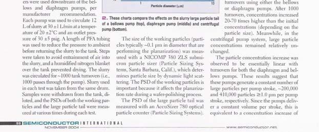
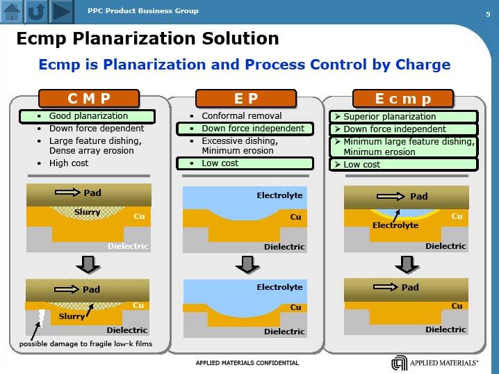
16 November 2004: Slurry Pumping


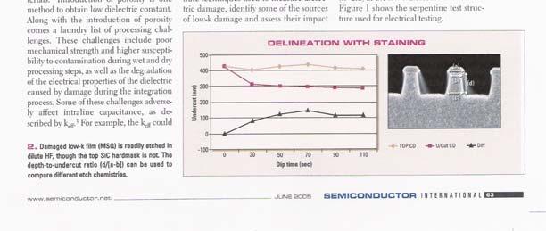
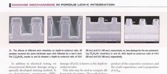
17 June 2005: Low-k Damage

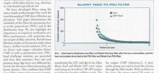
18 August 2005: Slurry Filtration
19 Cu/Low-k Integration Issues that Impact Performance and Reliability Issue Tradeoffs Example This Work ~ C Polish stop TDDB, erosion vs. C -10% Etch stop Rs tolerance -10% Cap thickness, k E-M, T/C, via-yields vs. C -10% SiCOH damage S-M, E-M, CD, strip vs. C -5% CD control TDDB, RIE/strip vs. C -15% Via heights T/C, yields vs. C -5% D. Edelstein, IEEE IITC (2004). The challenge: retain a manufacturable process with minimal capacitance and maximal reliability No poisoning, plasma damage, CMP damage, residual moisture, CD control problems, defects, etc. Webcast: Advanced Material Solutions for Interconnects, Semiconductor International, 9/13/06

20 November 2006: Outsourcing
21 Critical Factors for Any CMP Process Wafer / Materials Parameters Size / Shape / Flatness Film Stack Composition Metals (Al, Cu, W, Pt, etc.) Oxide (TEOS, PSG, BPSG, etc.) Other (polysilicon, low-k polymers, etc.) Film Quality Issues Stress (compressive or tensile) Inclusions and other defects Doping or contaminant levels Final Surface Requirements Ultralow surface roughness Extreme planarization, esp. Copper Low defectivity at <0.12 um defect size Pad Issues Materials (polyurethane, felt, foam, etc.) Properties must be chosen for the job Conditioning method often not optimized Lot-to-lot consistency Slurry Issues Chemistry optimization often required Mixing and associated inconsistency Shelf life and pot life sometimes very short Slurry distribution system (design, cost, upkeep) Agglomeration and gel formation Filtration is often required Cleaning method specific to slurry and film Waste disposal and local regulations Process Issues Long list of significant input variables Downforce Platen speed Carrier speed Slurry flow Conditioning method Disk used (material, diamond size, spacing, etc) Force Speed Sweep profile Highly sensitive to local pattern variation Must maintain consistency at high throughput Must optimize for variation of incoming films Integration Issues Materials Compatibility Electrochemical interactions with two or more metals Film integrity and delamination, esp. low-k Film stack compressibility Interactions with adjacent process modules Photolithography Metal deposition and metal etch Dielectric deposition and etch Electrical design interactions Feature size constraints Interactions with local pattern density Line resistance variation, esp. damascene copper Dielectric thickness variation Contact resistance variation Development and manufacturing teams must achieve technical performance requirements while balancing complexity, cost, risk and timelines.

22 The Future Thank You!