QUANTAX CrystAlign. Innovation with Integrity. Reinventing EBSD EBSD
|
|
|
- Vernon Bryant
- 5 years ago
- Views:
Transcription

1 Reinventing EBSD QUANTAX CrystAlign Innovation with Integrity EBSD


2 CrystAlign the User-friendly EBSD System Bruker s QUANTAX CrystAlign EBSD analysis system is the easy-to-use, multi-purpose tool for users of all levels. CrystAlign offers the versatility and flexibility for the investigation of all kinds of crystalline materials, whether standalone or in full integration with Bruker s QUANTAX EDS for combined EBSD and EDS analysis. The high performance e Flash EBSD detector series is a vital part of the package. Bruker has taken great care in the design of the e Flash detector series. The result of decades of experience in the development of electron microscopy equipment and in the needs of users associated with it, these detectors display outstanding usability and safety features and support the whole range of EBSD applications from high speed to high resolution and high sensitivity. Indexing speed and precision of the e Flash 1000 The e Flash 1000 for maximum speed The e Flash 1000 is currently the fastest detector in the market by far. In 8x8 binning mode the detector provides unparalleled 850 patterns/s. Using 4x4 binning mode 630 patterns/s can be acquired, the speed normally expected as maximum from other EBSD systems running in 8x8 binning mode. This detector impressively demonstrates that speed, accuracy and precision can be attained simultaneously. Accurate phase discrimination is guaranteed even at the highest acquisition speed. Precision in orientation determination is also a standard feature of the e Flash This can be taken from the misorientation plot in the figure on the right. Operating at its native resolution (640 x 480 pixels) the e Flash 1000 can acquire 210 patterns/s. Top: Austenite sample measured at full speed (620 patterns/s) with 4x4 binning. The misorientation plot along the white line (insert) shows orientation noise of only 0.4. Bottom: Raw map (no data cleaning) of an austenite sample, obtained at 845 patterns/s with only 2.7% zero solutions.


3 Excellence in EBSD detector manufacture: The Bruker e Flash series The e Flash HR maximum resolution detector The highest speed detector in the market is complemented by the highest resolution detector available. Bruker s e Flash HR detector operates with a native resolution of 1600x1200 pixels providing pattern images with incredible detail. Its pattern resolution and ultra-high signal sensitivity make the e Flash HR the detector of choice for difficult materials analysis tasks, like low beam current operation low kv operation poorly conducting samples nanomaterials analysis of pseudosymmetries lattice strain investigation In its native resolution the detector operates at speeds of up to 35 pattern/s. At maximum binning (20x20) the e Flash HR reaches a speed of 170 patterns/s. This makes it the fastest high resolution detector currently available. The vertical shift of the screen, accomplished by tilting the detector, allows to capture the optimum signal. The tilt angle is read out automatically and considered in detector calibration. Vertical screen positioning is also a precondition for producing the best possible measurement conditions during simultaneous EBSD and EDS acquisition. e Flash HR high resolution EBSD patterns In-situ adjustment of the vertical screen position The capability of vertical screen positioning under vacuum and when the detector is in working position is a unique feature of the e Flash detectors. This provides unprecedented flexibility in measurement setup and user comfort. As the spatial distribution of backscattered electrons depends on many factors, e.g. working distance and density, it is very convenient to have a mechanism to compensate the effects induced by the change of these parameters. Top: High resolution pattern of pyrite (iron sulfide, FeS 2). Bottom: Detail of the pyrite pattern.

 cables for signal transfer and detector control, the third is for power supply.")


4 Vertical screen adjustment The center image shows the raw image produced by an optimally positioned screen. Left and right the screen is either too low or too high. This will result in noisy pattern images in the bottom, or, the top half respectively after processing. Unique safety features The e Flash detectors have a closed encasement with all moving parts inside, which practically excludes all injury through moving parts. The detector is connected with three cables only, two Ethernet (RJ45) cables for signal transfer and detector control, the third is for power supply. Cable entanglement is avoided as the cables are stationary. A bright blue LED screen position indicator on the top of the encasement is always visible, even if the detector is switched off. This helps reduce the risk of screen damage through collision with parts in the SEM chamber. In the event of a collision the fast retraction mechanism will trigger immediately and move the screen out of the chamber with a high speed of 10 mm/s. Nevertheless, should the screen be damaged, it can be easily replaced by the user. Flexibility to suit any analytical environment and task The maximum insertion length of the e Flash detectors fits even the largest SEM chambers. The fast detector movement and positioning accuracy are very useful for repetitive tasks like 3D EBSD.
 and backscattered electron detectors (above the screen) is optimally aligned with respect to the sample, capturing maximum signal.")

 detectors above the phosphor screen provide a phase density signal, where the SEM s built-in BSE detector is likely to fail due to adverse geometrical conditions")

5 The revolutionary ARGUS forescattered / backscattered electron imaging system Forescattered electron detectors add color to microstructures Left: The imaging system using forescattered (below the screen) and backscattered electron detectors (above the screen) is optimally aligned with respect to the sample, capturing maximum signal. Center: Backscattered electron image of a high speed steel, showing matrix and precipitates. The precipitates appear bright due to their higher density. Right: Color coded orientation contrast image of the same area of a high speed steel sample, using forescattered electron detectors to show microstructural detail. The e Flash series is now optionally available with the ARGUS forescattered / backscattered imaging system (e Flash / e Flash HR+ ). The backscattered electron (BSE) detectors above the phosphor screen provide a phase density signal, where the SEM s built-in BSE detector is likely to fail due to adverse geometrical conditions during EBSD analysis. The three FSD detectors arranged horizontally below the phosphor screen are a novel design. As the forescattered electrons carrying the orientation information are distributed highly anisotropically, the three detectors are likely to register different intensities. Automatic setup and color coding produce high contrast colorful images showing even the slightest orientation change. Image acquisition is as fast as BSE detection. All electronics are inside the detector housing, ensuring minimal signal loss. This color adds information to microstructures The ARGUS FSE detectors produce colors where traditional detectors only show greyscale images. Naturally, any orientation difference will be much easier to detect in color coded images produced by the ARGUS, as the colorful image of a nickel sample shows.

6 ESPRIT Software for EBSD During the development of a complex analytical system like CrystAlign the biggest challenge is to simplify but not limit the operation so that both experienced and novice users are able to control the acquisition and post-processing software with ease and maximum efficiency. Two main approaches have been chosen to implement this goal: First, automatic features that take care of time-consuming tasks and simplify operation, and second, all analytical techniques are integrated under a single user interface unifying the operation of all software components. Signal Assistant The Signal Assistant is an automatic software tool that sets the camera to the optimum exposure time to obtain the necessary pattern quality to provide the best available conditions for band detection. Of course manual adjustment is also possible. The determined settings are stable and readjustment is only necessary if beam energy or detector and sample position have been altered. If pattern resolution (binning) is changed the acquisition time is adapted automatically. Complicated calibration is a thing of the past For a correct interpretation of the diffraction pattern one needs to know the so-called pattern center. Its determination is referred to as calibration. Knowledge of the pattern center is essential for deriving a crystallographic orientation with maximum precision and for correct phase discrimination. CrystAlign is the only EBSD system that can work in an auto calibration mode using a calibration method known as Iterative Pattern Fitting. CrystAlign automatically reads out tilt and detector position. In exceptional cases, where these parameters are not available, the Calibration Assistant allows manual entry. This assistant uses the current sample, no standard is required. Re-calibration is only necessary if the geometric setup (excluding working distance) is changed. If a measurement is launched with the wrong calibration values, CrystAlign allows an offline re-calibration and the subsequent correction of the EBSD data set. Functional principle of the Signal Assistant 1. Raw signal optimization Underexposed Optimized raw image Overexposed 2. Pattern image processing Image with optimally illuminated and resolved pattern


7 Screenshot of the versatile Calibration Assistant. Get started immediately No unanswerable questions asked Other commercially available EBSD analysis systems may require additional information from the user before data acquisition can be started. This information, e.g. number of bands to be used for indexing, Hough resolution, accuracy limits for simulated and experimental pattern comparison, etc., may be difficult to provide, even for the experienced user. This is especially the case if unknown phases are involved. Built for speed Should the region of interest be smaller than the field of view or irregularly shaped, an arbitrary region can be selected for analysis. This feature is also useful for minimizing drift phenomena. EBSD map of a resin-embedded copper wire With CrystAlign the additional setup is limited to the selection of phases, all other information is derived automatically from this selection. Actually, it is even possible to start a measurement without knowing a single phase beforehand. Detected band positions can be used for pattern interpretation including calibration after acquisition, without restrictions.


8 Pattern streaming for maximum speed and flexibility The term pattern streaming describes the process of temporary storage of an EBSD pattern and optionally an EDS spectrum for each measured point of a map in a single file on a storage medium, which is unique to CrystAlign. This allows live display of the collected experimental data during acquisition. After finishing the measurement CrystAlign offers the user the option to save patterns and / or spectra together with band positions, phase and orientation information. Alternatively experimental data can be deleted and only solutions saved, as commonly done. Keeping the experimental data is very useful for subsequent band detection and/or spectra quantification using different approaches. Moreover, if unknown phases are present it would be very helpful to use the original patterns during the offline phase identification procedure. Advanced pattern interpretation The secret of success of an EBSD system consists of correct band detection combined with a robust indexing algorithm. If a local orientation determination fails it mostly happens along grain or phase boundaries where patterns are superimposed. Since in this case detected bands belong to both patterns the assignment to a certain orientation/phase is not that simple anymore. CrystAlign uses robust band detection and indexing algorithms that rarely fail, even at high speed settings or in case of overlapping patterns. These are the most important prerequisites for correct interpretation of orientation data. This means that CrystAlign does not require data cleaning for the majority of applications, which always carries the risk of false or skewed data. Seamless integration for comfortable operation The two different but complementary techniques, i.e. EBSD and EDS, are fully integrated in the ESPRIT software suite allowing the operator to execute different analytical tasks without constantly switching between programs. Impressive indexing accuracy Left: Raw data of a high speed orientation map of austenitic steel (630 patterns/s, 4x4 pixel binning, 0.1 % zero solutions). Right: Enlargement of the white frame in the left image, clearly showing that indexing is as accurate along grain or phase boundaries as it is within grains.

9 Fast and fully integrated EBSD and EDS: Combined measurements with ease A single mouse click changes between EBSD and EDS analysis or between different tasks in the EBSD workspace. The combination of the two techniques on the same software platform also leads to increased productivity through higher speed, improved data quality and above all processing and understanding results is much easier. Fast simultaneous EBSD/EDS measurements for efficient materials characterization State of the art high throughput SDD EDS detectors combined with innovative ideas in transferring/saving data enable simultaneous EBSD/EDS measurements at very high speeds. For instance, when using the XFlash 5030 EDS detector, automatic mapping is now possible at speeds of up to 520 points/s. CrystAlign saves the phase/orientation information delivered by the EBSD system as well as a complete EDS spectrum for each point in a map. The richness of information provided by the two techniques combined with the processing speed of the Cryst- Align software makes the Bruker EBSD/ EDS system a very powerful tool for characterizing materials. Thus, simultaneously acquired EBSD/EDS data sets can be used for: EDS-based phase discrimination possessing an extremely fast quantification procedure the CrystAlign software can use the EDS information to distinguish between phases producing similar EBSPs; this option can be used, practically without slowing down the system, on the fly during data acquisition or offline during re-analysis Offline phase identification using an advanced interactive phase identification procedure the user can easily identify missing/unexpected phases. The raw data can subsequently be re-analyzed using the complete/ corrected phase list. Due to incredible re-analysis speeds, which can be up to two orders of magnitude faster than a completely new measurement, the re-analysis procedure will take no more than a few seconds or minutes. This procedure can be done offline without further occupying the SEM. Valuable additional information through simultaneous EBSD/EDS measurements Left: Raw as acquired phase map of a friction-welded Cu-Al bar. Most of the map was indexed as Al (blue) although only the upper right corner actually is Al. The misindexing occurs because Cu and Al are practically indistinguishable by EBSD alone. Right: Final phase map after offline identification and re-analysis with EDS quantification for Al (blue) and Cu (red) for phase discrimination. Do also note the discovery of an additional intermetallic phase (Al 4Cu 9, green) through the offline identification.

10 Detailed crystallographic information is always only a mouse click away Incredibly fast re-indexing Using a sophisticated indexing algorithm and the full power of modern programming techniques CrystAlign is capable of re-indexing EBSD data sets at incredible speeds. Thus, single phase maps can be re-indexed with up to 54,000 points/s. CrystAlign is currently the only system where simultaneous indexing of multiple phases during data collection does not slow down the analysis speed significantly. Another big advantage of this fast indexing is that data sets can be re-analyzed extremely fast. The most common practical example is when phase identification has to be re-done offline after realizing that one or more additional phases might be present in the map just acquired. After identifying all present phases fast re-indexing will allow the completion / correction of a data set without the need to re-acquire data, thus keeping the SEM free for other tasks. Easy access to all measurement information The user can switch between two standard EBSD workspace displays. In acquisition mode it contains the SEM image, the phase list and a freely adaptable area for maps and point information. Screenshot of the EBSD user interface in acquisition mode, displayed is a map of duplex steel containing four phases. Superimposed in the upper left is the local interpretation dialog. In this case it displays the experimental pattern and the found solution at the current cursor position (see mouse pointer in the large map). The pattern on the right is not a second experimental pattern but a dynamic diffraction theory simulation (displayed in real time). Please note the impressive accuracy of this simulation method.

11 A variety of options for checking the quality of acquired data have been included, providing full confidence in the analysis results. The user has real time access to numerous details on any point in the map, either during measurement or offline on a loaded map. The local interpretation dialog box provides the following information at the cursor position in a map: Experimental pattern, detected bands and corresponding solution drawn in the color of the respective phase 3D view of the unit cell orientation (Orientation) Hough transform of the pattern and detected peak positions (Hough) EDS spectrum (in case of simultaneous EBSD/EDS data acquisition) Simulated patterns based on kinematic and dynamic (option) theories. Additionally, the pattern quality index and the Euler angles are displayed as figures. In evaluation mode the shared workspace enables useful interactions between orientation maps and orientation presentation tools like pole figures, inverse pole figures (IPF) or ODFs. Thus, orientation distributions displayed for each selected phase are linked to the simultaneously shown EBSD map. The orientation of a pixel in the map where the mouse pointer is currently over is automatically highlighted in each pole figure. An info bar containing miniatures of all available mapping representations can be found below the map window. Clicking on the miniature displays the corresponding map in the large results window. Many orientation presentation options are provided for a profound interpretation of a data set, e.g. pattern quality map, inverse pole figure maps, Euler angle maps, Schmid factor map, different misorientation maps, grain and phase boundary The EBSD workspace in evaluation mode simultaneously displays overlaid maps and pole figures. All figures are automatically updated during measurement.

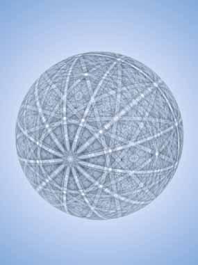
12 descriptions, but also numerous other tools like histograms reflecting e.g. the grain size distribution for each phase. Similar miniatures can be found beneath the pole figures window as well. Here the user can add self-defined pole figures and IPFs. The selectable tabs enable access to the information specific to each phase. The predefined pole figures are phase and Laue group specific and already show the orientation distribution of relevant poles. 3D pole figures All maps and pole figure representations are dynamically refreshed during acquisition. Both maps and pole figures can be displayed in full screen mode. Alternatively to the pole figure representation in 2D CrystAlign can display pole figures also in 3D as projection onto a unit sphere. This supports the conception of the density distribution of each lattice plane {hkl} since the spheres rotated in real-time give a fast and undistorted overview of the orientation distribution. Advanced user-friendly phase editor and phase search For the successful use of EBSD the crystallographic description of the investigated phases is essential. Therefore, CrystAlign also contains a powerful phase editor which provides the user with full access to all relevant crystallographic data. The main characteristic of this phase editor is the simultaneous visualization of the spatial distribution of atoms in the unit cell and the resulting EBSD pattern. The representations of diffraction patterns and crystal structures are linked so that during real-time rotations the user can see why certain bands appear stronger than others. The band intensity simulation is based on the kinematic theory and it includes an improved model for band brightness prediction, especially where bands cross. The simulated EBSD patterns can be displayed as a projection on a sphere or Alternative representations of pole density distributions for different lattice planes projected on a sphere. The small transparent sphere in the lower right shows the sample reference coordinate system, X (red), Y (green) and Z (blue). as a projection onto a screen, so that they appear like experimental patterns. The Hough transform derived from the simulated pattern is also available to support the understanding of band detection and pattern interpretation. CrystAlign is shipped with a representative cross section of the ICSD (Inorganic Crystal Structure Database) consisting of more than 3400 phases as well as a Bruker phase database containing entries for the most common phases. Of course, new phase files can be created and existing files can be modified and saved as desired. CrystAlign is *.cif -compatible (Crystal Information File), enabling the user to import any phase file from databases available free of charge, like the American Mineralogist Crystal Structure Database. Even direct import of cry-files
 is possible.")
 is simple and straightforward.")
13 Phase editor dialog showing the crystallographic details of the Sigma intermetallic phase as well as the corresponding crystal structure, spherical EBSP and the reflector list. ( HKL Technology) is possible. Editing the phase list before launching a measurement can easily be done, either by searching for phases inside a crystallographic database, loading a saved phase list or by loading a *.cif file, previously downloaded from the Internet. Searching for a phase in the crystallographic database(s) is simple and straightforward. The search can be done based on name, chemical composition and/or crystal symmetry. Phase search dialog showing the various options available when searching for phases in a crystallographic database, e.g. ICSD.

14 Realistic pattern simulation Viewer for simulated EBSD patterns showing the projection on a sphere for cementite. A double click on the sphere will change the display to gnomonic projection, equivalent to experimental patterns. It is a fact well known among experts that EBSD patterns clearly show dynamic effects in their intensity distribution, which are caused by multiple scattering and diffraction within a crystal. Until recently this phenomenon was ignored in the simulation of EPSPs because of its complexity, and the time needed for a single diffraction pattern simulation was in the scale of many hours to days. A simplified kinematic approach was and is still used instead, accepting the disadvantage that it can provide wrong results for complex cases of phase identification. It ignores the higher order effects as well as the fact that bands may cross. This is problematic, especially when dealing with more complex phases. Treading new paths for the advance of science and technology Bruker has known about these problems since its involvement in the EBSD field and seen the great potential that lies in their solution. This led to the development of a set of algorithms for pattern simulation according to dynamic theory. The results of this development are overwhelming: not only could the simulation be sped up greatly, but the simulated patterns are much richer in detail and closer to reality than those by any other simulation method. The biggest difference to conventional (kinematic) pattern simulation lies in vastly improved band intensity predictions. Also the brightness distribution across bands is far more realistic. Still, Bruker uses an improved algorithm based on kinematic theory for fast intensity prediction.
 as an option to its analytical software package.")
 takes from several seconds to a few minutes only. The actual duration depends on several factors, e.g. the complexity of the crystal structure and excitation conditions.")

15 Bruker is proud to be the first and at the date of publication of this brochure only supplier of commercially available EBSD software to have included realistic intensity prediction (dynamic pattern simulation) as an option to its analytical software package. Easy and comfortable operation Pattern simulation is possible for any three-dimensional periodic crystal structure available in a suitable database, e.g. ICSD, American Mineralogist, etc. An entire simulation (not only a single pattern) takes from several seconds to a few minutes only. The actual duration depends on several factors, e.g. the complexity of the crystal structure and excitation conditions. Moreover, once calculated the pattern can be displayed/ rotated in real time as spherical EBSP as well as single pattern projections that resemble experimental data. Parameters can be set to match experimental conditions. These are the acceleration voltage, pattern resolution and the number of reflectors. In the userfriendly style of CrystAlign, numerous phase-specific presets are used for all other parameters which are hard to predict, even for an expert user. Benefits for novices and experienced users The simulated EBSD patterns can be used for convenient evaluation of experimentally collected data and the derived orientation. In general, the simulation is extremely useful since it is the only way to become familiar with the formation of EBSD patterns, and to recognize key factors, e.g. by varying the numerous parameters to be considered. Also, simulations once made for specific experimental conditions are stored and can be retrieved for unlimited reuse without re-calculation. In summary, dynamic pattern simulation is useful for Fundamental understanding of EBSD pattern formation, regarding information depth energy distribution Extraction of real band intensities indexing for crystallographically more complex phases Pseudo-symmetries Generation of reference patterns for phase verification & identification point group determination (e.g. polar direction, etc.) lattice strain approximation Comparing different simulations with the experiment Fast intensity prediction Experimental pattern Realistic intensity prediction Comparison between experimental data and simulated patterns using kinematic (fast) and dynamic diffraction theory (realistic).

16 All configurations and specifications are subject to change without notice. Order No. DOC-B82-EXS002, Rev Bruker Nano GmbH. Printed in Germany. Technical Specifications Excellent speed, accuracy and sensitivity... In-situ vertically adjustable detector for maximum analytical flexibility (WD) in optimized signal conditions Independent data acquisition, pattern streaming with up to 630 patterns/s (4x4 binning) or 850 patterns/s (8x8 binning) using the fast e Flash 1000 detector Ultra-sensitive high resolution EBSD detector e Flash HR delivering EBSPs with 1600x1200 pixels when used in its native resolution mode; maximum speed of 170 patterns/s at 20x20 binning Simultaneous EBSD and EDS data acquisition at speeds of up to 520 points/s (recommended combination with the high throughput XFlash 5030 EDS detector) ARGUS, high-sensitivity optional FSE/BSE imaging system delivering high detail color coded orientation contrast images as well as phase contrast images State of the art optical system for minimal EBSP distortion High accuracy software controlled detector positioning for precise fully automatic calibration Improved signal and higher speed through rectangular phosphor screen design, screen mounted on a tapered frame allowing simultaneous EBSD/EDS measurements with close detector/ sample distance LED phosphor screen position indicator and various other safety features All electronics inside the detector housing no external moving parts Bruker Nano GmbH Berlin Germany Phone +49 (30) Fax +49 (30) info@bruker-nano.de Bruker Nano Ewing, NJ USA Phone +1 (609) Fax +1 (609) info@bruker-nano.com Sales representative: