nitride (% 300A) around the island sidewalls such oxide recessed below the silicon active regions, beak local oxidation process can be realized
|
|
|
- Phyllis Sanders
- 5 years ago
- Views:
Transcription

1 THE SWAMI - A DEFECT FREE AND NEAR-ZERO BIRD'S-BEAK LOCAL OXIDATION PROCESS AND ITSAPPLICATION INVLSI TECHNOLOGY K.Y. Chiu*, R. Fang*, 3. Lin*, J.L. Moll*, C. Lage**, S. Angelos**, R. Tillman** * Hewlett Packard Laboratories, Palo Alto, California, ** Hewlett Packard Company, Corvall is, Oregon, nitride ABSTRACT at the foot of island sidewalls. A new SWAMI scheme is presented which takes full ad- A new scneme for SWAMI (Side fll1 Masked vantage of LOCOS processing without suffering the - Isolation) process is presented which takes difficulties. The modified SWAMI process incorfull advantage of LOCOS processing without porates a sloped sidewall and a layer of thin suffering the difficulties. The new SWAMI nitride (% 300A) around the island sidewalls such technology incorporates a sloped silicon side- that both intrinsic nitride stress and volume exwall and thin nitride around the island side- pansion induced stress are greatly reduced. A walls such that both intrinsic nitride stress defect free and near-zero bird's-beak local oxidaand volume expansion induced stress are greatly tion process, with more than 70% of the field reduced. A defect free and near-zero bird's oxide recessed below the silicon active regions, beak local oxidation process can be realized can be realized by the SWAMI. by the SWAMI. Fabrication technology and MOSFET electrical characteristics will be dis- This paper describes the new SWAMI fabrication cussed. A SWAWI/CMOS circuit including 60K process, the device electrical characteristics, and ROM, 2.5K SRAM, and 100 segments of display its impact on scaled VLSI technology. A P-well driver with 5.13 x 5.22 m2 chip size has been CMOS circuit including 60K ROM, 2.5K SRAM, and 100 successfully fabricated. The results indicate segments of display driver with 5.13 x 5.22 mm2 that the SWAMI is capable of replacing the chip size fabricated with the SWAMI isolation LOCOS as the isolation technology for scaled process is also presented. VLSI circuit fabrication. The SWAMI Isolation Process INTRODUCTION As device geometries are scaled down to Table I outlines the sequence of steps in the the micrometer and submicrometer range, a new fabrication process to form the new SWAMI isolaisolation technology to provide the smallest tion structure. The process is identical to the pattern transfer difference between rrask and conventional ful ly-recessed oxidation process active device geometry for any giving lithoexcept that steps (6) through (10) are added to graphic technique is required. It is desirable form this near-zero bird's-beak and defect free that the new isolation technology have the isolation scheme. In order to avoid the formation following properties: 1) defect free; 2) require of a thick nitride layer perpendicular to the no scaling down of the field oxide thickness as silicon substrate and around the island sidewalls, other geometries are scaled down; 3) planar a C2F6 plasma was employed to etch nitride, oxide, surface; 4) require no additional photomasking and single crystal silicon in one operation after steps; and 5) compatible with existing LSI island patterning. Figure 1 exhibits the etching processing techniques. characteristics of Cz F6 plasma. The sloped sidewall on (100) single crystal silicon can also be A sidewall masked isolation technology obtained by a KOH wet etching. Figure2 illustrates (SWAMI) was reported [l] by empl'oying anisotropic schematically the major processing steps of the silicon and silicon nitride etching to form a new SWAMI approach. After island patterning and C2Fs bird's-beak free isolation structure. The SWAMI plasma etching of nitride/oxide/silicon, process is compatible with the conventional channel stop boron was implanted. A layer of LPCVD oxide was deposited, as shown in Figure 2(b), after LOCOS [2] and has a zero bird's-beak and a second stress relief oxide wasgrown and the second nearly planar surface. However, due to the nitride was deposited. The LPCVD oxide serves as nature of the vertical sidewalls in the original a mask for second nitride SWAMI structure, the thickness of the second etching such that thin second nitride on sloped sidewall can be implenitride in the direction perpendicular to sub- mented without additional photomasking steps. strate is actually very thick. This nitride, After ani sotropi c plasma (C 2F6) oxi de/ni tri de around the sidewalls of the island region, forms etching and wet oxide etching to remove the LPCVD a rigid film perpendicular to the silicon sub- oxide ribbon around the island sidewalls, the thin strate. It was found [3] that the original second nitride remains around the sloped sidewall SWAMI is vulnerable to the formation of dis- and extends into the planar field regions as locations during field oxidation due to volume shown in Figure 2(d). During field oxidation, expansion from oxide intrusion under the second IEDM 82 CH1832-5/82/ $ IEEE

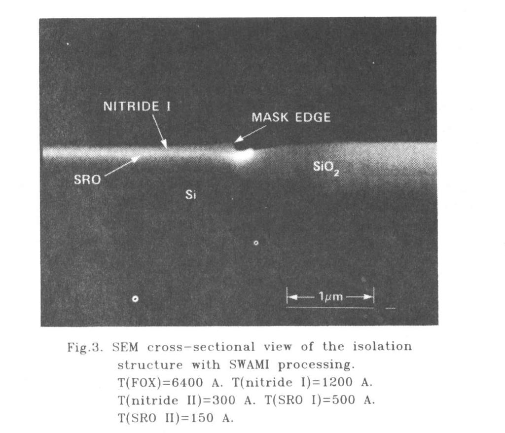
2 the thin nitride layer on the sloped sidewall wil be pushed up due to volume expansion of the oxide without causing large stress acting on the silicon substrate. The new SWAMI provides the flexibility of using relatively thinner nitride and thicker stress relief oxide such that the intrinsic nitride stress can be drastically reduced. No oxide re-fill and etch-back are required. Due to the sloped silicon sidewalls, channel stop boron can be implanted onto the silicon sidewalls such that no double threshold voltage effect occurs at the corner of the islands [4,5]. Figure 3 shows an SEM cross-sectional view of the isolation structure with SWAMI processing after growth of 640 nm of field oxide at 900 OC in steam anhient The length of the bird's-beak can be controlled to less than 0.1 um for a field oxide thickness thicker than 0.8 um, and more than 70% of the fie1 d oxide is recessed below island surface. Devi ce Characteristics After the SWAMI isolation structure was formed, an NMOS polysilicon gate process was employed to fabricate MOSFET's. Process parameters are listed in Table 11. After MOSFET devices are fabricated, temperat.wre-bias stressed C-V and breakdown voltage of gate oxide capacitors were measured to investigate the integrity of the final gate oxide in terms of its stability of the interface charges, the breakdown field, and the defect density of the thin gate oxide. Test capacitor structure was designed with very long island edges to investigate the effect of island sidewalls on the integrity of gate oxide. Test results indicate that both fixed charge and mobile charge densities are approximately at 3E10/cm2. The histogram of the measured gate breakdown voltage is shown in Figure 4. The 25 nm gate oxide with the SWAMI isolation process has defect density below 10 defects/cm2. As mentioned earlier, defect generation during field oxidation is one of the major concerns of the sidewall masked isolation process. The defects, usually edge dislocations, are likely to cause higher diode junction leakage by providing deep recombination centers especially by attracting heavy metal impurities. Therefore, it is importdnt to measure leakage current of diodes fabricated with the SWAMI process and compare it with diodes fabricated with the LOCOS process. Figure 5 shows the diode leakage current as a function of junction temperature for three different kinds of diodes. The finger diode has the same planar area planar diode except that the total length of the as the island edges is more than 10 times longer. AS discussed previously, if there are any extra defects generated from the SWAMI process they Wil be generated along the island edges. Since firlger diode has longer island edges, it wil have higher leakage current than the planar diode and diodes fabricated with the SWAMI wil have higher leakage current than diodes fabricated with the Test results indicate that almost all three different diodes have identical leakage Current LOCOS. Wi th activation energy of 1.1 ev, which is thediffusion limited leakage current. The diode leakage current measurement confirms that the SWAMI process does not generate any extra defects as compared to the LOCOS process. Measurements of turn-on behavior of gate transistor with mask layout dimensions of W/L=1/2 um is shown in Figure 6. No double threshold voltage occurs in this subthreshold curve. The subthreshold slope obtained from this transistor is approximately 80 mv/decade. The turn off characteristics of polysi 1 i con-gated parasi ti c field oxide device with layout spacing of Zmicrons is shown in Figure 7. The turn-off rate of field transistor is about 550 mv/decade. There is little difference in transisqor turn on/off behavior for devices fabricated with the SWAMI or with the LOCOS process. The feasibility of the SWAMI isolation process for VLSI circuit fabrication has been successfully verified by fabricating a P-well CMOS ci rcui t with reasonable.yield. This CMOS ci rcui t, ashown in Figure s(a.1, contains 60K ROM, 2.5K SRAM, and 100 segnrelits of display driver with 5.13 x 5.22 mm2 chip size. Figure 8(b) illustrates the cross-sectional view of the device structure in this circuit. It shows the improvement in surface planarity over devices fabricated with the LOCOS. CONCLUSION A defect free and near-zero bird's-beak local oxidation process has been successfully demonstrated by the SWAMI. This new isolation process features: defect free, simple process, planar surface topology, no additional masking step is required, and its process is compatible with existing LSI processing techniques. It offers several advantages over the conventional LOCOS processing such as: (a) near-zero bird's-beak; (b) no scale down of field oxide thickness is required as other device geometries are scaled down, and (c) planar surface topology. These advantages not only enhance VLSI circuit performance and packing density, but also improve the production yield especially when device feature size is shrinking down below one -micron level. ACKNOWLEDGMENT The authors would like to thank the entire staff of HP IC Processing Laboratory for processing the wafers. Thanks are due to Fred Schwettmann and Bob Grimm for their support and encouragement during the course of this work. REFERENCES (1) K.Y. Chiu, J.L. Moll, J. Manoliu, "A Bird's Beak Free Local Oxidation Technology Feasible for VLSI Circuits Fabrication," IEEE Trans. Electron Devices, ED-29, 536, IEDM
3 (2) J.A. Appels, E. Kooi, MM. Paffen, J.J.H. Schatorji, W.H.C.G. Verkuylen, "Local Oxidation of Silicon and its Application in Semiconductor Device Technology," Philips Research Reports, Vol. 25, No. 2, pp. 118, 1970, (3) R.C.Y. Fang, K.Y. Chiu, J.L. Moll, "Defect Characteristics and Generation Mechanism in a Bird's Beak Free Structure by Sidewall Masked Technique," Accepted for publication in J. Electrochemical Society. (4) T. Iizuka, K.Y. Chiu, and J.L. Moll, "Double Threshold MOSFET's in Bird's Beak Free Structure," IEEE IEDM Tech. Dig., Paper #16.3, Table II. Process parameters of NMOS/SWAMI devices Field oxide : 700 nm Gate oxide : 25 nm Field implant : B+, 7OKev, 3E12/cm2 Channel implant : B+, BOKev, 9Ell/cm2 Gate electrode : N+, 350 nm S/D junction : 250 nm THE SWAMI (5) K. Kurosawa, T. Shibata, and H. Iizuka, "A New Bird's Beak Free Field Isolation Technology for VLSI Devices," IEEE IEDM Tech. Dig., Paper , Table I. Sequence of processing steps in SWAMI approach (1) Grow stress relief oxide (SRO I) (2) Deposit LPCVD nitride (nitride I) (3) Pattern island region (mask I) (4) Plasma etch nitride I, SRO I, and silicon step (in one operation) (5) Channel stop field implant (B+) (6) Grow stress relief oxide (SRO 11) (7) Deposit second nitride (nitride 11) (8) Deposit LPCVD oxide (9) Plasma etch LPCVD oxide and second nitride in one operation (no mask) (10) Wet etch LPCVD oxide (11) Grow field oxide (12) Strip nitrides (chemical) m PHOTORESIST 1 A c SI02 SI (100) (dl... (e) 3-E (1) SlO2 j '. SlO, Fig.2. The major processing steps of the SWAMI. (a). After island patterning and etching. (b). After nitride I1 and LPCVD oxide deposition. (c). After plasma oxidebitride etching. (a). Island structure before field oxidation. (e). After field oxidation. (f). Final isolation structure. C2 F6 PLASMA ETCH RATE SI H/rn,n SISN, : looo~lm~n SI (100) : 3008/mm AZ RESIST: ~ 1 ~ ~ ~ Fig.1. C2F6 plasma etching characteristics Flg.3. SEM cross-sectional view of the isolation structure with SWAMI processing. T(FOX)=6400 A. T(nitride 1)=1200 A. T(nitride 11)=300 A. T(SR0 I)=500 A. T(SR0 II)=l50 A IEDM 82
4 TOTAL NUMBER OF CAP4CITORS = 1.8 x 10⁻¹ Plll2 L = Ljcm [,$PI****** GRAPHICS PLOT X***** I os SWAMI GATE TRANSiSTOR ( A) Go?e oxide : 25 nm 1/2 ~lln I I 0 IO G4TE BREAKDObN VOLTAGE IVOIISI decade1 /dlv -1.o F~g.4. Histogram of gate oxlde breakdown voltage. lol, 90 C 70 C 25% c PLANAR DIODE 1 1 ~:f672~~0- Cm OFINGER DIODE {t ;:2i:m10- cm.finger DIODE WITH LOCOS IO VGS.2000/d1v ( V) Fig.6. Subthreshold curve of enhancement gate transistor. T(FOX)=7000 A, T(GOX)=250 A. IPAI IO -- IO -- [hp]****** GRAPHICS PLOT ****** I os SWAMI FIELD TRANSISTOR 100/2 dm ( A) Fieid oxide : 700 im IOOOlT Fig.5, Dmde leakage current versus Junctlon temperature. Fig.7. Turn-off behavior of parasitic field transistor. Fig.8. (A). Photomicrograph of CMOS circuit containing 60K ROM, 2.5K SRAM, and 100 segments of display driver. Chip size is 5.13 * 5.22 mm2. (B). SEM cross-sectional view of device structure with SWAMI processing. T(poly)= 500 nm, T(Fox)=BOOnm,and T(Gox)=dOnm. IEDM
5