Oki M A-60J 16Mbit DRAM (EDO)
|
|
|
- Baldric Lawson
- 5 years ago
- Views:
Transcription
1 Construction Analysis Oki M A-60J 16Mbit DRAM (EDO) Report Number: SCA Global Semiconductor Industry the Serving Since N. Hartford Drive Scottsdale, AZ Phone: Fax: Internet:
2 INDEX TO TEXT TITLE PAGE INTRODUCTION 1 MAJOR FINDINGS 1 TECHNOLOGY DESCRIPTION Assembly 2 Die Process 2-3 ANALYSIS RESULTS I Assembly 4 ANALYSIS RESULTS II Die Process and Design 5-7 ANALYSIS PROCEDURE 8 TABLES Overall Evaluation 9 Package Markings 10 Wirebond Strength 10 Die Material Analysis 10 Horizontal Dimensions 11 Vertical Dimensions 12 - i -
3 INTRODUCTION This report describes a construction analysis of the 16Mbit DRAM. Two devices which were encapsulated in 28-pin small-outline packages with J-leads (SOJs) were received for the analysis. No date code was decipherable (1996?). MAJOR FINDINGS Questionable Items: 1 Metal 2 aluminum thinned up to 95 percent 2 at most vias. The barrier metal remained intact to provide continuity. Special Features: Bit line over capacitor stacked cell design. Textured poly capacitor plates. 1 These items present possible quality or reliability concerns. They should be discussed with the manufacturer to determine their possible impact on the intended application. 2 Seriousness depends on design margins
4 TECHNOLOGY DESCRIPTION Assembly: 28-pin small-outline plastic packages with J-leads (SOJs). LOCEB (lead-on-chip, edge bonded) leadframe design. A double backed adhesive tape connected the leadframe to the die surface. A polyimide die coat was present over the die surface. Lead-locking provisions (anchors) were present at all pins. Multiple bonding wires were used at pins 1, 14, 15 and 28 to provide additional current-carrying capacity to the power buses. All pins were connected. Dicing was by sawing (full depth). Wirebonding was by the thermosonic ball bond method using 1.0 mil O.D. gold wire. Die Process and Design: The 16Mbit DRAM was organized as 2,097,152 words x 8 bits. The device features fast page mode of operation with EDO. Devices were fabricated using a selective oxidation CMOS process with N-wells in a P-substrate. It is believed a twin-well process was employed; however, the P-well could not be delineated. No epi was present. A patterned polyimide die coat was present to protect against packaging stresses. Final passivation consisted of a single layer of nitride
5 TECHNOLOGY DESCRIPTION (continued) Two levels of metal were used. Both employed aluminum with titanium-nitride (TiN) caps and barriers. Metal 1 also employed a titanium adhesion layer. Both metal levels were defined using a dry-etch technique. Standard vias were used between metal 2 and metal 1. Tungsten plugs were used as the vertical interconnect under metal 1. Intermetal dielectric consisted of two layers of silicon-dioxide. The second layer of glass had been subjected to an etchback. No spin-on-glass (SOG) was employed. Pre-metal dielectric consisted of three layers of reflow glass and densified oxide. The glass was reflowed prior to contact cuts. One additional layer was present in the array. Four levels of dry-etched polysilicon were used. Poly 1 (poly and tungsten silicide) formed all gates on the die. Poly 2 and 3 were used exclusively in the cell array. Poly 2 was used to form the individual plates of all capacitors. This poly layer was textured to increase the capacitor surface area. Poly 3 formed the common plate of the capacitors. Poly 4 (poly and tungsten silicide) formed the bit lines in the array and was used throughout the die as an interconnect layer. N+ and P+ implanted source/drain diffusions formed N- and P-channel transistors. All gates used oxide sidewall spacers that were left in place. The memory cells used an NMOS DRAM cell design consisting of a select gate and a stacked capacitor. Poly 1 formed the word lines/select gates and was piggybacked by metal 1. Stacked capacitors were formed by poly 2 plates covered by a poly 3 sheet separated by a thin dielectric. The poly 2 plate was textured providing increased area (capacitance). Poly 4 formed the bit lines. Redundancy was implemented using poly 4 fuses. Laser blown fuses were noted on both samples inspected. Cutouts were present above fuse locations
6 ANALYSIS RESULTS I Assembly: Figures 1-4 Questionable Items: 1 None. Special Features: LOCEB leadframe design. General Items: 28-pin small-outline plastic packages with J-leads (SOJs). All pins were connected. Overall package quality: Normal. No defects were noted on the external portions of the package. No voids or cracks were noted in the plastic material. Leadframe: LOCEB leadframe design. No header/paddle was used. Pin condition was good, intact solder coating externally and silver spot plating internally. Lead-locking design: Good. Anchors were present at all pins. Wirebonding: Thermosonic ball bonds using 1.0 mil O.D. gold wire. No bond lifts occurred and bond pull strengths were normal (see page 10). Bonding wire spacing was good, no excessive wire sweep. Multiple bonding wires were present at pins 1 and 14 (Vcc) and 15 and 28 (Vss) to provide additional current-carrying capacity to the power buses. Die dicing: Die separation was by sawing with normal quality workmanship. No large chips or cracks were noted. A patterned polyimide die coat was present over the surface of the die. 1 These items present possible quality or reliability concerns. They should be discussed with the manufacturer to determine their possible impact on the intended application
7 ANALYSIS RESULTS II Die Process: Figures 4-45 Questionable Items: 1 Metal 2 aluminum thinned up to 95 percent 2 at most vias. Barrier metal maintained continuity. General Items: Fabrication process: Selective oxidation CMOS employing twin-wells in a P substrate (no epi). Process Implementation: Die layout was clean and efficient. Alignment was good at all levels. No damage, process defects, or contamination was found. A patterned polyimide die coat was employed. Final Passivation: Single layer of nitride. Integrity tests indicated defect-free passivation. Edge seal was good. Metallization: Two levels of metallization were used. Metal 2 consisted of aluminum with a titanium-nitride (TiN) cap and barrier. Metal 1 consisted of aluminum with a titanium-nitride cap and a titanium-nitride on titanium (Ti) barrier/adhesion layer. Standard vias were used as the interconnect between metal 1 and metal 2. Tungsten (W) plugs were used under metal 1. 1 These items present possible quality or reliability concerns. They should be discussed with the manufacturer to determine their possible impact on the intended application. 2 Seriousness depends on design margins
8 ANALYSIS RESULTS II (continued) Metal patterning: Both metal levels were defined by a dry etch of good quality. Metal 2 was widened around vias. All vias were completely surrounded by metal. Metal one design rules were fairly aggressive providing a 1.3 micron pitch with 0.45 micron wide metal lines in the array. Metal defects: No notches or voids were noted in either metal layer. Fairly large silicon nodules were found during cross sectioning. They occupied in excess of 90 percent of the metal line thickness (Figure 20). Metal step coverage: Metal 2 aluminum thinned up to 95 percent at most vias. The barrier aided in retaining the connections. Metal 1 thinned up to 50 percent at some contacts. The tungsten plugs were fairly level with the oxide surface, so no large steps were present for the metal to cover. Via and contact defects: Some minor over-etching of was noted under tungsten plugs, however; no problems are foreseen. Intermetal dielectric: This dielectric consisted of two layers of silicon-dioxide. The second layer had been subjected to an etchback for planarization. No spin-on-glass was employed between these layers. Pre-metal dielectric: The dielectric between metal 1 and poly 4 consisted of a BPSG reflow glass and was reflowed prior to contact cuts. An additional layer of this material was present between poly 4 and poly 3, and yet another between poly 2 and poly 1. No problems were found. Polysilicon: Four levels of dry-etched polysilicon were used. Poly 1 (poly and tungsten silicide) formed all gates on the die. Poly 2 and 3 were used exclusively in the cell array. Poly 2 was used to form the individual plates of all capacitors. This poly layer was textured to increase the capacitor surface area. Poly 3 formed the common plate of the capacitors. Poly 4 (poly and tungsten silicide) formed the bit lines in the array and was used throughout the die as an interconnect layer
9 ANALYSIS RESULTS II (continued) Isolation: Local oxide (LOCOS). No problems were present, and no step was found at the well boundaries. Diffusions: Implanted N+ and P+ diffusions formed the sources and drains. The process employed oxide sidewall spacers that were left intact. No problems were found. Wells: N-wells were employed in a P substrate. It is believed that the P-well could not be delineated in the P substrate. Epi: No epi layer was employed. Redundancy: Redundancy was implemented by laser blowing poly 4 fuses. Passivation and intermetal dielectric cutouts were present above fuse locations. Buried contacts: Direct poly 4-to-N+ diffusion (buried) contacts were present throughout the die. In addition, poly 2 made direct contact to N+ in the cell array. Memory cells: Bit line over capacitor DRAM cell design consisting of a select transistor with a stacked capacitor as the storage element. Poly 1 was piggybacked by metal 1 to form the word lines/select gates. Poly 2 (textured) and the poly 3 sheet formed the plates of the storage capacitor. Poly 3 also distributed memory enable throughout the cell array. Poly 4 formed the bit lines. Cell size was 1.25 x 2.6 microns (3.25 microns 2 ). This is considered quite large for a 1996 era design
10 PROCEDURE The devices were subjected to the following analysis procedures: External inspection X-ray Decapsulation Internal optical inspection SEM of assembly features and passivation Wirepull test Passivation integrity test Passivation removal SEM inspection of metal 2 Delayer to metal 1 SEM inspection of metal 1 Delayer to poly and inspect poly structures and die surface Die sectioning (90 for SEM) * Measure horizontal dimensions Measure vertical dimensions Die material analysis * Delineation of cross-sections is by silicon etch unless otherwise indicated
11 OVERALL QUALITY EVALUATION: Overall Rating: Normal/Poor DETAIL OF EVALUATION Package integrity Package markings Die placement Die attach quality Wire spacing Wirebond placement Wirebond quality Dicing quality Wirebond method Die attach method Dicing method N N G N G G N N Thermosonic ball bonds using 1.0 mil gold wire. Double backed adhesive tape. Sawn Die surface integrity: Toolmarks (absence) Particles (absence) Contamination (absence) Process defects (absence) General workmanship Passivation integrity Metal definition Metal integrity 2 Metal registration Contact coverage Contact registration N N N N N G G NP N N N 2 95 percent metal 2 aluminum thinning, and fairly large silicon nodules in both metals. G = Good, P = Poor, N = Normal, NP = Normal/Poor - 9 -
12 PACKAGE MARKINGS OKI JAPAN M A-60J A9Z WIREBOND STRENGTH Sample 1 Wire material: 1.0 mil diameter gold (Au) Material at package lands: silver (Ag) # of wires tested: 14 Bond lifts: 0 Force to break - high: 10g - low: 7.5g - avg.: 8.4g - std. dev.: 1.5 DIE MATERIAL ANALYSIS Final passivation: Metallization 2: Intermetal dielectric: Metallization 1: Plugs: Pre-metal glass: Silicide on poly 4: Silicide on poly 1: Nitride. Aluminum with a titanium-nitride cap and barrier. Two layers of silicon-dioxide. Aluminum with a titanium-nitride cap and titanium-nitride/titanium barrier/adhesion layer. Tungsten. BPSG. Tungsten. Tungsten
13 HORIZONTAL DIMENSIONS Die size: 6.9 x 15.4 mm (271 x 606 mils) Die area: 106 mm 2 (164,664 mils 2 ) Min pad size: 0.12 x 0.12 mm (4.8 x 4.8 mils) Min pad window: 0.11 x 0.11 mm (4.3 x 4.3 mils) Min pad space: 0.06 mm (2.2 mils) Min metal 2 width: 1.4 micron Min metal 2 space: 1.6 micron Min metal 2 pitch: 3.0 microns Min via size: 1.4 micron (dia.) Min metal 1 width: 0.45 micron Min metal 1 space: 0.7 micron Min metal 1 pitch: 1.3 micron Min metal 1 contact: 0.6 micron (dia.) Min poly 4 width: 0.35 micron Min poly 4 space: 0.8 micron Min poly 4 contact: 1.0 micron (dia.) Min poly 1 width: 0.3 micron Min poly 1 space: 0.6 micron Min diffusion space: 0.7 micron Min gate length * - (N-channel): 0.45 micron - (P-channel): 0.55 micron Cell size: 3.25 microns 2 Cell pitch: 1.25 x 2.6 microns * Physical gate length
14 VERTICAL DIMENSIONS Die thickness: 0.35 mm (13.8 mils) Layers Passivation: Metal 2 - cap: 0.7 micron 0.12 micron - aluminum: 0.65 micron - barrier: 0.12 micron Interlevel dielectric - glass 2: Metal 1 - cap: Contact plugs: 0.5 micron (average) - glass 1: 0.4 micron 0.12 micron - aluminum: 0.5 micron - barrier/adhesion layer: 0.1 micron Pre-metal dielectric: Poly 4 - silicide: Poly 3: Poly 2: micron 0.4 micron (average) 0.1 micron - poly: 0.1 micron Poly 1 - silicide: 0.1 micron 0.05 micron (approx.) 0.1 micron - poly: 0.1 micron Interpoly dielectric - LOCOS: - poly 4 - poly 3: 0.5 micron (average) - poly 2 - poly 1: 0.3 micron 0.4 micron N+ S/D diffusion: 0.2 micron P+ S/D diffusion: 0.3 micron N-well: 3.3 microns (approx.)
15 INDEX TO FIGURES ASSEMBLY Figures 1-4 DIE LAYOUT AND IDENTIFICATION Figures 5-8 PHYSICAL DIE STRUCTURES Figures 9-45 REDUNDANCY FUSES Figures COLOR DRAWING OF DIE STRUCTURE Figure 32 DRAM MEMORY CELL STRUCTURES Figures CIRCUIT LAYOUT AND I/O Figures ii -


16 Figure 1. Package photographs of the. Mag. 4.2x.

17 PIN 1 Figure 2. X-ray view of the package. Mag. 8x.


18 DIE Mag. 140x EDGE OF PASSIVATION Mag. 960x Figure 3. SEM views illustrating dicing and edge seal. 60.


19 PLASTIC PACKAGE POLYIMIDE DIE COAT Mag. 800x DIE DIE COAT EDGE OF PASSIVATION Mag. 3200x DIE COAT BOND PAD Mag. 3200x DIE Figure 4. SEM section views illustrating the edge seal and polyimide die coat.

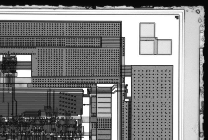
20 Figure 5. Portion of the whole die photograph. Mag. 26x.

21 Figure 6. Remaining portion of the whole die photograph. Mag. 26x.


22 Figure 7. Optical views of die markings. Mag. 600x.


23 Figure 8. Optical views of die corners. Mag. 150x.


24 PASSIVATION METAL 2 W PLUG METAL 1 LOCOS N+ S/D POLY 1 GATE PASSIVATION METAL 1 POLY 4 POLY 1 W PLUG glass etch Figure 9. SEM section views illustrating general structure. Mag. 6500x.


25 Mag. 3000x Mag. 12,000x Figure 10. SEM views illustrating final passivation. 60.


26 PASSIVATION METAL 2 INTERLEVEL DIELECTRIC Mag. 13,000x PASSIVATION TiN CAP ALUMINUM 2 TiN BARRIER Mag. 26,000x Figure 11. SEM section views of metal 2 line profiles.


27 METAL VIAS Figure 12. Topological SEM views of metal 2 patterning. Mag. 3000x, 0.


28 Mag. 4000x Mag. 4000x TiN CAP Mag. 13,500x ALUMINUM 2 TiN BARRIER Figure 13. Perspective SEM views of metal 2 step coverage. 60.


29 METAL 2 ILD METAL 1 TiN/Ti BARRIER Mag. 26,000x PASSIVATION 95% THINNING ALUMINUM 2 TiN BARRIER ALUMINUM 1 TiN CAP Mag. 52,000x Figure 14. SEM section views illustrating a via and interlevel dielectric composition.


30 METAL 1 ILD POLY 4 Mag. 26,000x TiN CAP DELINEATION ARTIFACT ALUMINUM 1 TiN BARRIER Ti ADHESION LAYER Mag. 52,000x Figure 15. SEM section views of metal 1 line profiles.


31 POLY 4 VIAS Mag. 3200x METAL 1 CONTACTS Mag. 5000x Mag. 6500x Figure 16. Topological SEM views of metal 1 patterning. 0.


32 POLY 4 Mag. 8000x METAL 1 Mag. 8000x TiN CAP ALUMINUM 1 Mag. 30,000x TiN BARRIER W PLUG Figure 17. Perspective SEM views of metal 1 step coverage. 60.


33 METAL 1 W PLUG POLY 4 METAL 1 W PLUG REFLOW GLASS POLY 1 LOCOS Figure 18. SEM section views illustrating typical metal 1 contacts. Mag. 26,000x.


34 METAL 1 W PLUG LOCOS POLY 4 P+ Mag. 13,000x METAL 1 W PLUG POLY 1 GATE N+ S/D Mag. 26,000x Figure 19. Additional SEM section views of typical metal 1 contacts.


35 PASSIVATION METAL 2 Si ILD METAL 1 Si W PLUG Figure 20. SEM section views illustrating silicon nodules in the aluminum. Glass etch, Mag. 26,000x.


36 POLY 1 INTERPOLY CONTACTS POLY 4 BURIED CONTACTS Figure 21. Topological SEM views of poly 4 patterning. Mag. 3200x, 0.


37 Mag. 6000x Mag. 7000x POLY 4 Mag. 28,000x Figure 22. Perspective SEM views of poly 4 coverage. 60.


38 POLY 4 POLY 1 LOCOS POLY 4 LOCOS N+ S/D POLY 1 Figure 23. SEM section views illustrating typical poly 4 contacts. Mag. 26,000x.


39 W SILICIDE SIDEWALL SPACER LOCOS POLY 4 POLY 1 GATE POLY 4 POLY 1 LOCOS Figure 24. SEM section views illustrating typical poly 4 contacts. Glass etch, Mag. 26,000x.


40 Mag. 3200x P+ Mag. 3200x N+ POLY 1 Mag. 6500x Figure 25. Topological SEM views of poly 1 patterning. 0.


41 Mag. 7000x Mag. 8000x POLY 1 GATE LOCOS Mag. 28,000x Figure 26. Perspective SEM views of poly 1 coverage. 60.


42 POLY 1 GATE N-channel N+ S/D GATE OXIDE POLY 1 GATE SIDEWALL SPACER P-channel P+ S/D POLY 1 W SILICIDE SIDEWALL SPACER glass etch Figure 27. SEM section views of typical transistors. Mag. 52,000x.


43 POLY 1 LOCOS GATE OXIDE Figure 28. SEM section view of a typical birdsbeak. Mag. 52,000x. AREA SHOWN BELOW DELINEATION ARTIFACT optical, Mag. 1500x N-WELL P-SUBSTRATE REFLOW GLASS LOCOS SEM, Mag. 13,000x N+ GUARDBAND N-WELL Figure 29. Section views illustrating well structure.


44 CUTOUT Mag. 620x CUTOUT BLOWN FUSE Mag. 1200x Figure 30. Optical views of typical fuses.


45 INTACT FUSE BLOWN FUSE Mag. 1600x PASSIVATION CUTOUT Mag. 3200x Figure 30a. Topological SEM views of typical fuses. 0.


46 LASER BLOWN FUSE Mag. 2000x PASSIVATION CUTOUT Mag. 4000x Figure 31. Perspective SEM views of typical fuses. 60.
47 REFLOW GLASS W SILICIDE POLY 4 PRE-METAL GLASS TiN CAP TiN CAP ALUMINUM 2 TiN BARRIER TiN BARRIER Ti ADHESION LAYER W SILICIDE PASSIVATION ALUMINUM 1 INTERLEVEL DIELECTRIC,,,,,,,, PRE-METAL GLASS,,,,,,,,,,,,,,,, N+ S/D P-WELL W PLUG LOCAL OXIDE P SUBSTRATE P+ S/D Orange = Nitride, Blue = Metal, Yellow = Oxide, Green = Poly, Red = Diffusion, and Gray = Substrate Figure 32. Color cross section drawing illustrating device structure. POLY 1 N-WELL


48 PIGGYBACK WORDLINE metal 1 MEMORY ENABLE BIT LINE poly 4 Figure 33. Perspective SEM views of the DRAM cell array. Mag. 8000x, 60.


49 POLY 3 SHEET poly 3 POLY 1 WORD LINE poly 2 and poly 1 Figure 34. Perspective SEM views of the DRAM cell array. Mag. 8000x, 60.
 POLY 1 poly")


50 poly 4 poly 3 POLY 2 (TEXTURED) POLY 1 poly 2 and poly 1 Figure 35. Detailed perspective SEM views of the DRAM cell array. Mag. 20,000x, 60.


51 POLY 2 PLATE POLY 1 WORD LINE Mag. 40,000x POLY 2 PLATE POLY 1 WORD LINE LOCOS Mag. 52,000x Figure 36. Detailed SEM views of the textured poly 2 plates. 60.


52 PIGGYBACK WORD LINE metal 1 BIT MEMORY ENABLE poly 4 Figure 37. Topological SEM views of the DRAM cell array. Mag. 6500x, 0.


53 MEMORY ENABLE poly 3 POLY 1 POLY 2 POLY 1 WORD LINE poly 2 and poly 1 Figure 38. Topological SEM views of the DRAM cell array. Mag. 6500x, 0.


54 BIT poly 4 BIT MEMORY ENABLE poly 3 Figure 39. Topological SEM views of a DRAM cell. Mag. 26,000x, 0.

55 C 1 BIT WORD BIT 1 C MEMORY ENABLE Figure 40. Topological SEM view and schematic of a DRAM cell. Mag. 26,000x, 0.


56 METAL 1 PIGGYBACK WORD LINE POLY 4 BIT LINE Mag. 13,000x LOCOS N+ S/D POLY 1 SELECT GATE POLY 4 BIT LINE POLY 3 SHEET POLY 2 PLATE LOCOS Mag. 26,000x POLY 1 SELECT GATE CAPACITOR DIELECTRIC POLY 3 SHEET POLY 2 PLATE Mag. 52,000x N+ S/D Figure 41. SEM section views of the DRAM cell array (parallel to bit line).


57 POLY 4 BIT LINE POLY 4 BIT LINE CONTACT LOCOS N+ Mag. 13,000x POLY 4 BIT LINE POLY 4 BIT CONTACT POLY 3 SHEET N+ LOCOS Mag. 26,000x Figure 42. SEM section views of the DRAM cell array (perpendicular to bit lines).


58 METAL 1 PIGGYBACK WORD LINE POLY 4 BIT LINE Mag. 13,000x POLY 1 WORD LINE POLY 4 BIT LINE POLY 3 SHEET Mag. 26,000x LOCOS POLY 1 WORD LINE POLY 3 SHEET Mag. 52,000x POLY 2 PLATE LOCOS N+ Figure 43. SEM section views of the DRAM cell array (perpendicular to bit lines).


59 Mag. 300x Mag. 600x Figure 44. Optical views of typical circuitry and input protection.


60 PASSIVATION METAL 1 Mag. 6500x W PLUG POLY 1 GATE N+ S/D METAL 1 REFLOW GLASS POLY 1 GATE Mag. 13,000x N+ S/D REFLOW GLASS POLY 1 GATE Mag. 26,000x N+ S/D N+ S/D Figure 45. SEM section views of typical I/O structure.