Cleanroom, Wafer Clean and Gettering
|
|
|
- Melissa Blair
- 5 years ago
- Views:
Transcription


1 Principles of Micro- and Nanofabrication for Electronic and Photonic Devices Cleanroom, Wafer Clean and Gettering Xing Sheng 盛兴 Department of Electronic Engineering Tsinghua University 1

2 Integrate Circuits Moore's law transistor number transistor size 5


3 Technology Evolution 1947 today 1 cm < 100 nm 6

4 Factory Evolution cost of new fab million $ today billion $ Video TSMC < 100 nm 2016 长江存储, 武汉 24 billion $$ 7
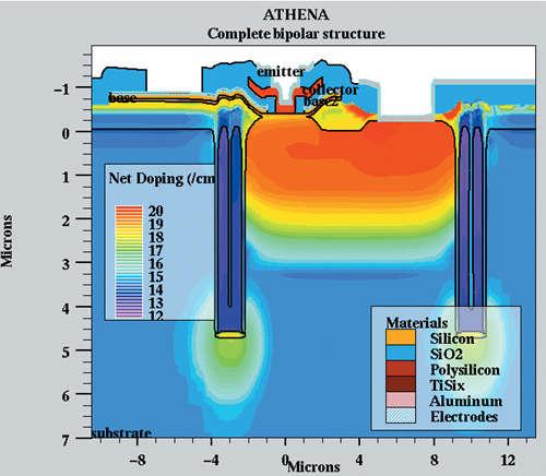
5 Process Simulations Silvaco 8

6 Manufacturing Yield Yield: rate of success assume yield = 99% per step: = = 0.02 every 1% yield means $$$ 9
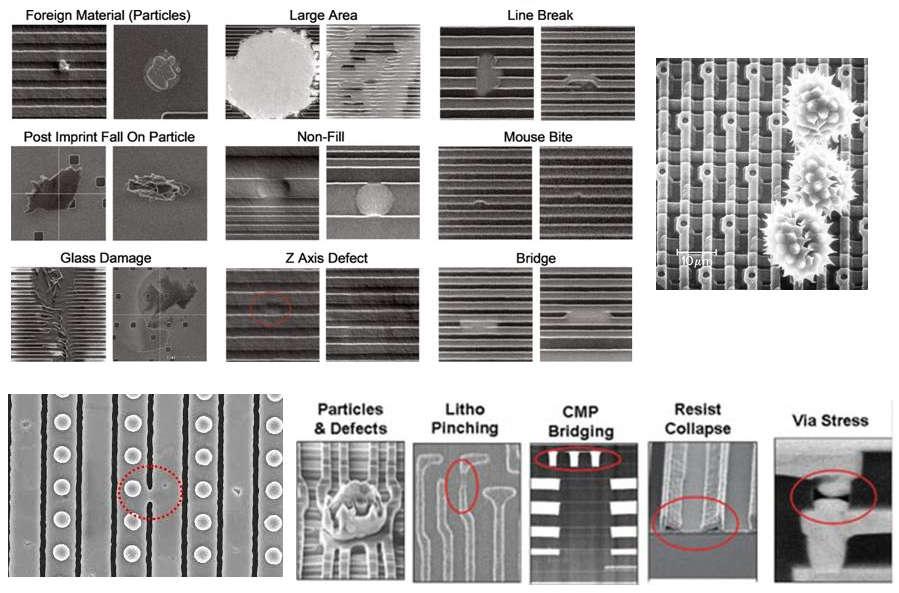
7 Manufacturing Defects 10

8 Defects in Silicon 11
9 Defects in Silicon Q: why? dopants deep level defects Na, K, Au, Cu, Fe, O,... 12


10 Defects in Silicon ions in gate oxide deep level defects in Si dopants 13
11 Defects in Silicon Deep level defects (e.g. Au) reduce minority carrier lifetime in Si bad for solar cells 14

12 Defects recombination at defect sites reduce efficiencies of LEDs / solar cells 15
 J D diffusion flux (mol/m 2 /s) diffusivity (m 2 /s)")
13 Diffusion of Defects Liquid Solid C concentration (mol/m 3 ) J D diffusion flux (mol/m 2 /s) diffusivity (m 2 /s) 16
14 Diffusion of Defects Diffusivity ( 扩散系数 ) D rate of spread unit: cm 2 /s fast D D 0 exp( E A kt ) Diffusion length L slow L Dt Q: why? diffusivity of defects in Si 17

15 Defect Diffusivity in Silicon Si, B, P, As, Sb,... Cu, Fe, Li, H, Au,... Slow Fast 18
 in gate oxide 19")
16 Defects in Oxide V th V FB 2 f 2 qn s C A ox (2 f ) qq C M ox defect density Na, K,... alkali ions (Na, K,...) in gate oxide 19
17 Defects on Surface E bd (MV/cm) E bd (MV/cm) Surface roughness (nm) Surface roughness (nm) Surface roughness reduces breakdown voltages (E bd ) 20
18 Defects Control environment cleanroom control surface clean Si wafer gettering 21

19 Contaminations particles: - hair - pollen - bacteria - PM chemicals: - organics - Cu, Au - Na, K

20 Sources of Contaminations particles from human sitting 100,000 /min walking 1,000,000 /min running 10,000,000 /min 23

21 Particles 24

22 IC Roadmap 25
23 Cleanroom class X: less than X particles larger than 0.5 m per cubic feet 26
24 Cleanroom class X: less than X particles larger than 0.5 m per cubic feet 27

25 Cleanroom 'PM2.5 index' << 1 g/m 3 class X: less than X particles larger than 0.5 m per cubic feet 28
26 Defects Control environment cleanroom control surface clean Si wafer gettering 29
 5 10 13 15 leakage current (A/m 2 ) 12*10-9 10*10-9 5*10-9")
27 Defects in Water defects in water effects of water cleaning on transistor performance water resistivity (M*cm, at 25 o C) leakage current (A/m 2 ) 12* *10-9 5*10-9 1*
28 Water Types purified water, distilled water, tapping water,... 自来水, 矿泉水, 纯净水, 超纯水, 蒸馏水,... In cleanroom, deionized (DI) water ( 去离子水 ) is used free of any mineral ions only H +, OH - In water, at 25 o C H 2 O <-> H + + OH - [H + ]*[OH - ] = K w = (mol/l) 2 in DI water, [H + ] = [OH - ] = 10-7 mol/l, ph = 7.0 resistivity = 18.5 M*cm 31


29 Si Wafer Clean Ultrasonic / megasonic clean in DI water remove: large particles, water soluble ions (Na, K, Cl,...) 32
30 Standard Si Wafer Clean (RCA) Step 1 (SC-1) Step 2 NH 4 OH : H 2 O 2 : H 2 O = 1:1:5, at 80 o C, 10 mins remove organic residues HF : H 2 O = 1:50, at 25 o C, 20 secs remove native SiO 2 Step 3 (SC-2) HCl : H 2 O 2 : H 2 O = 1:1:6, at 80 o C, 10 mins remove metals Step 4 clean in DI water 33
31 Metal Removal 34
 clean H 2 O + O 3 remove organic residues Organic solvent Acetone / Isopropanol / DI water remove organic residues not used for standard CMOS process!")
32 Other Si Clean Recipes Piranha clean SPM: Sulfuric-Peroxide Mixture H 2 SO 4 : H 2 O 2 = 3:1, mins extremely exothermic, self heating up to 80 o C remove organic residues and some metals Ozone (O 3 ) clean H 2 O + O 3 remove organic residues Organic solvent Acetone / Isopropanol / DI water remove organic residues not used for standard CMOS process! 'wet' method 35


33 Other Si Clean Recipes UV Ozone clean clean organic residues Plasma clean clean organic residues 'dry' method 36
34 Clean other Materials SiO 2 (glass, quartz,...) GaAs piranha clean, H 2 SO 4 : H 2 O 2 = 3:1, mins SC-1, NH 4 OH : H 2 O 2 : H 2 O = 1:1:5, at 80 o C, 10 mins NH 4 OH : H 2 O = 1:10, for stoichiometric surface (Ga/As 1:1) H 3 PO 4 or HCl, for As rich surface Acetone / Isopropanol / DI water generally works well for most non-cmos process 37
35 Surface Roughness Surface roughness (nm) Surface roughness (nm) Surface Roughness of Si after cleaning ammonia (NH 4 OH) and HF slightly etches Si 38
36 Defects Control environment cleanroom control surface clean Si wafer gettering 39

37 Gettering( 吸杂 ) 'gettering' in the vacuum tube use titanium to absorb gases in vacuum tubes titanium 40

38 Si Wafer Gettering( 吸杂 ) intrinsic gettering extrinsic gettering: Si 3 N 4, P 2 O 5,... 41
 intrinsic gettering")

39 Si Wafer Gettering( 吸杂 ) intrinsic gettering easy hard O defects in Si diffusivity of defects 42
40 Si Wafer Gettering( 吸杂 ) Minority carrier lifetime Au doped Si: Typical Si: Gettered Si: 10-9 s 10-6 s 10-3 s 43
41 Principles of Micro- and Nanofabrication for Electronic and Photonic Devices Lab Safety Xing Sheng 盛兴 Department of Electronic Engineering Tsinghua University 44


42 Lab Safety Chemicals HF, H 2 SO 4,... KOH, NH 4 OH,... Acetone,... Electricity instruments,... Fires Acetone, Alcohol,... Sharps... silicon, glass,... 45


43 Lab Safety Lab orientation exits, showers,... Proper protection gloves, goggles, aprons,... Materials Data Safety Sheets (MSDS)... 46


 47")
44 Lab Safety Materials Data Safety Sheets (MSDS) 47


45 Chemical Safety NFPA diamond 0: no hazard 4: highest risk HF acetone H 2 O 2 48
 slowly etches glass HF strongly etches glass!")
46 Chemical Safety Choose proper containers Most solvents glass, Teflon,... Be careful alkali (NaOH, etc) slowly etches glass HF strongly etches glass! glass art by HF etch 49


47 Chemical Safety glass art by HF etch 50

48 Radiation Safety XRD SEM & TEM Ebeam Evaporator 51


49 Laser Safety wear goggles Q: O.D. 52
50 Biological Safety 53

51 Cleanroom Orientation Video always gown up! 54

52 Process References 55