3. Photolithography, patterning and doping techniques. KNU Seminar Course 2015 Robert Mroczyński
|
|
|
- Agatha Lloyd
- 5 years ago
- Views:
Transcription

1 3. Photolithography, patterning and doping techniques KNU Seminar Course 2015 Robert Mroczyński
2 Critical technology processes Photolithography The aim of this process is to transfer (in the most accurate way) of the mechanical quartz mask pattern to the mask material photoresist Photoresist is a material which protects (selectively) the underlaying material during subsequent processing step etching or implantation Etching The aim of this process is to transfer (in the most accuarte way) the pattern developed in the photoresist into underlaying material (dielectric, conductive, etc.) 2

3 Photolithography the idea M. Quirk, J. Serda; Semiconductor Manufacturing Technology 3
4 Classical (subtractive) method before the process after layer fabrication after photoresist coating after photolithography after etching after photerisist removal The development of selective remover/etchant is needed Problems with patterning of some conductive materials, e.g. Cu, Au, Pt 4
5 Additive ( lift-off ) method before the process after photoresist coating after photolithography after layer fabrication after lift-off The low-temperature layer fabrication and non-continuosity of layer are needed Lift-off procedure has to be highly selective to other materials present on the substrate 5
6 Photolithography modes Proximity Contact Projective (wafer stepper) 6
7 Double-side photolithography It was used for the first time in the course of MOEMS devices fabrication Two methods: Simultaneous exposure of both sides of semiconductor substrate Quasi-double-side photolithography -> the alignment of new objects with already fabricated onto other side of semiconductor substrate the method for look-up onto other side is crucial (e.g. in infrared light) 7
8 Photolithography summary UV Light HMDS Resist Mask 1) Vapor prime 2) Spin coat 3) Soft bake 4) Alignment and Exposure 5) Post-exposure bake 6) Develop 7) Hard bake 8) Develop inspect M. Quirk, J. Serda; Semiconductor Manufacturing Technology, Prentice Hall
9 Photolithography steps alignment Pattern on the substrate Mask Alignment of pattern on the quartz mask with pattern developed onto photoresist The alignment procedure occurs during the observation of patterns in the microscopy objectives In order to accurate alignemnt teh special alignment marks are needed they are located on particular plae in each IC module The first step is to align the angle between both patterns and the second step is to use apropriate movement in x and y directions 9
 Hg lamp M. Quirk, J.")
10 Relative Intensity (%) Photolithography steps exposure (nm) UV Visible light EUV VUV DUV Mid-UV Violet Blue Green Yellow Orange Red KrF laser i h g Excimer laser Hg lamps Wavelength (nm) Hg lamp M. Quirk, J. Serda; Semiconductor Manufacturing Technology 10
 and Depth of Focus (DOF) R = kλ NA We want to have the")
 the longer exposure time - + Depth of")
 2 R DOF 365 nm 0.45 486 nm 901 nm 365 nm 0.60 365 nm 507 nm 193 nm 0.")
11 The accuracy of petterning process Two parameters which describe the quality of photolithography process Resolution (R) and Depth of Focus (DOF) R = kλ NA We want to have the best R (smallest R) simultaneously with high DOF the compromise arises! Center of focus Lens The higher NA (numeric aperture) the longer exposure time - + Depth of Focus Photoresist Film R 365 nm nm 365 nm nm 193 nm nm 193 nm nm DOF = λ 2(NA) 2 R DOF 365 nm nm 901 nm 365 nm nm 507 nm 193 nm nm 476 nm 193 nm nm 268 nm 11
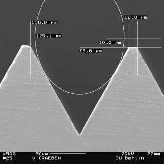
12 Resolution Rozdzielczość 365nm Patterning accuracy the gap between mask and photoresist s surface 5,0 3,3 1,7 1,0 0,8 0,7 0, Photoresist s Grubość fotorezystu thickness [µm] [µm] 3 µm 2 µm 1 µm 0,5 µm The obtaining of the lowest R (the smallest feature size) needs following: The minimalization of the gap between mask and photoresist s surface The minimalization of photoresist s thickness The minimalization of wavelenght 12
13 Rozdzielczość Resolution [µm] [µm] Patterning accuracy the gap between mask and photoresist s surface 2,0 1,8 1,5 1,3 1,0 zbliżeniowa proximity 0,5 365nm kontaktowa contact 0,8 kontaktowa 124nm 0, Grubość fotorezystu [µm] Photoresist s thickness [µm] 13
14 Etch selectivity Etch rate rate of material removal (e.g., nm/min) Relative (ratio) of the etch rate of the thin film to mask material, substrate or another film The ideal selectivity occurs when the desired material is only etched without any other materials removal 14

")
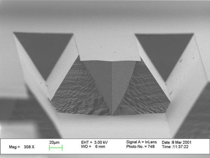
15 Etch anisotropy The etch rate ratio of particular material in both directions lateral and horizontal Isotropic etching the same etch rate in all directions characteristic for wet etching visible undercutting Anisotropic etching minimal undercutting with almost vertical sidewalls characteristic for dry (plasma) etching 15
16 Anisotropic etch perspectives Monocrystalline materials The presence of periodic structure results in intrinsic of distinguished etch direction Anisotropic etchant is needed Wet anisotropic, as well as dry etching process are possible in order to obtaine vertical sidewalls Polycrystalline and amorphous materials The lack of crystallographic order results in the same etch rate towards all direction The only solution for anistropic etching is the use of dry method 16
 Temperature Dopining concentration Chemical compounds based on: KOH (NaOH,")
) Silicon nitride the best masking material photoresist, as well as oxide")
17 Anisotropic wet etching of silicon (Si) The tech rate is dependent on: Crystalographic orientation (plane) Temperature Dopining concentration Chemical compounds based on: KOH (NaOH, CeOH, NH 4 OH, ) TMAH EDP (ethylenediamene pyrocatecol) N 2 H 4 (hydrazine) Used at the elevated temperature (~80 o C)) Silicon nitride the best masking material photoresist, as well as oxide is etched 17
18 18

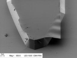
19 Anisotropic etching of amorphous materials Only anisotropic process allows for the full control of feature size, and thus, the device s dimensions Etching processes are of the most importance in the case of etching of windows with high aspect ratio - very important for MOEMS fabrication Dimensions of nowadays ICs do not allow for wet etching techniques -> the dry etching process is the only option 19
20 Anisotropy mechanisms Electric field it s arised between glow discharge (plasma) and bottom electrode where the silicon substrate is located A plasma is fully or partially ionized gas composed of equal number of positive and negative charges and a different number of unionized molecules A plasma is produced when an electric field of sufficient magnitude is applied to a gas which resuts in the gas breakdown and ionization The direction of electric field s lines is vertical to the semiconductor substrate Positive ions are accelerated and strike the substrate with high kinetic energy -> sputtering process physical etching Very anisotropic but small selective 20
21 Anisotropy mechanisms Anisotropy can be obtained also by a combination of chemical (chemical reaction on the surface) and physical (ion bombardment) etching Chemical etching etching done by reactive species such as free radicals Neutral or/and ionized species interact with the material s surface to form volatile products Another mechanism is the use of non-volatile fluorocarbon films that are deposited on the sidewalls Fluorocarbon films deposit on all surfaces but the ion velocity is vertical, and thus, as the etching proceeds there is a little ion bombardment of the sidewalls and the inhibitor film is accumulated 21

22 Reactive Ion Etching (RIE) Gas inlet ~ PLASMA R.F. generator with matching network Electrodes Cooled table To pumps Wafers with material to be etched lay on the smaller electrode Higher voltage drop near the lower electrode -> higher ion bombardment, more directional etch but less selectivity Physical and chemical etch component can be easily controlled by plasma chemistry Process parameters: Power Pressure Gas composition and flows Time Electrodes geometry 22

 etching (in")
23 Deep etching of silicon DRIE Deep RIE Process based on the two classical process PECVD and RIE RIE etching of non-covered by photoresist silicon surface (usually in SF 6 plasma) PECVD polymer deposition on silicon sidewalls the protection of sidewall against lateral (chemical) etching (in C 4 F 8 plasma) 23
24 Physical <-> chemical etching Wolf S., Tauber R.N.: Silicon Processing for the VLSI Era, Lattice Press, Sunset Beach, California
25 Silicon doping Semiconductors are not intrinsically conductive they are perfect materials totally useless in technology In order to make them conductive, the replace of silicon atoms with dopant atoms is needed doping process which is essential in ICs fabrication The dopant atom has to be characterized with fewer or more electrons on valence band than 4 of silicon 25
 then it is a DONOR atom, e.g.")
26 Silicon doping If atom has more electrons (e - ) then it is a DONOR atom, e.g. Phosphorus (P), Arsenic (As), Antymony (Sb) The extra e - is effectively released from the bonded atoms to join a cloud of free e - s, free to move like e - in a metal If atom has less electrons then it is a ACCEPTOR atom, e.g. Boron (B) lack of e - = hole (h + ) Si h + is a mobile (+) charge carrier Si Si Si Si + P Si Si Si Si + B Si P Si B Si Si extra free electron Si Si hole 26
27 Diffusion Movement of dopants within the silicon at high temperatures (950 o C or above) Three possible mechanisms (in Si): dopant Si Si Si Si Si Si Si Si vacancy Si Si Si Si Si Si Si Si Si Si Si Si Si Si Si Si Si Si Substitutional impurity atom moves along vacancies in the lattice Interstitial impurity atoms jump from one interstitial site to another Mixing impurity atom replaces a Si atom in the lattice Substitutes for a free Siatom place in the lattice Rapid diffusion hard to control and impurity not in lattice site not electrically active Si atom is displaced to an interstitial site 27
28 Masking during diffusion process 28

 GASEOUS inert gas (np. nitrogen, argon) dopants source (depending on dopants type e.g. POCl 3 or B 2 H 6 ) 29")
29 Diffusion process Furnace system using solid, liquid or gaseous dopants source SOLID Furnace system with heating Dopants source + inert gases To reactor LIQUID Diffusion stages: Glass deposition (phospho- or boron-silicate glass) Prediffusion (diffusion from unlimited source) Rediffusion (diffusion from limited source) GASEOUS inert gas (np. nitrogen, argon) dopants source (depending on dopants type e.g. POCl 3 or B 2 H 6 ) 29
30 Dopants profile after diffusion process Concentration Pre-diffusion Concentration Re-diffusion Time Time Depth Time Depth The result of diffusion process is described by a concentration of dopants and junction depth -> dopant profile 30
31 Diffusion s parameters Temperature Dopants source Source s parameters (temperature, composition, ) Composition and flows of inert gases Dopant is electrically active just after the diffusion process Each high temperature process occured after diffusion process can strongly influence onto dopant profiles! 31
32 Ion implantation M. Quirk, J. Serda: Semiconductor Manufacturing Technology, Prentice Hall, 2001 Ion source Plasma Extraction assembly Analyzing magnet Acceleration Ion beam column Process chamber 32
33 Implantation mechanism lectronic collision Energetic dopant ion Crystall lattice Si Si Si Si Si Si X-rays Si Si Si Si Si Si Atomic collision Si Si Si Si Si Displaced Si Si Si Si atom Si Si Si Si Charged dopant (ion) accelerated to high energy by an electric field (e.g. 100 kv) Control current and time to control the dose Depth determined by energy and type of dopant Semiconductor material damaged -> top surface becomes amorphous Ion collides with atoms and interacts in the lattice -> slow down and eventually stop -> statistical process, can be approximated by a Gaussian distribution Dopants not in the lattice sites -> not electrically active 33


34 Crystall lattice damage <100> <110> Light ion <111> Heavy ion chanelling M. Quirk, J. Serda: Semiconductor Manufacturing Technology, Prentice Hall,
35 Dopants profile after implantation Concentration Concentration Thin oxide material Dose Energy Depth Depth The possibility to obtain similar dopants prfile as in the diffusion case only by using thin dielectric material 35
36 Implantation s parameters Type of implanted ions Type of substrate (composition, crystallographic lattice, ) Energy of ions Implantation s direction Substrate s temperature Dopant is not electrically active just after the diffusion process! Post-implantation annealing process necessary in order to put dopants into lattice sides and rebuild damages of the substrate! 36
37 Diffusion <-> Implantation Diffusion Implantation Control of profile Very small Large Control of dose (+/- 20%) (+/- 1%) Substrate damage None Can be large Process temperature High Very low (but PIA needed) Junction s depth Large Can be very shallow Concentration s homogeneity Mask material Low Resistant of high temperature High Photoresist 37
38 Mask thickness [um] Mask thickness [um] Masks for doping processes 1 0,1 Oxide mask Boron Phosphorus 1 0,1 Photoresist Boron Phosphorus Arsenic 0, Diffusion time [min] 0, Energy [kev] 38
39 CMOS structure with doped regions p-channel Transistor n-channel Transistor p + LI oxide n + n + p STI n STI n STI p p + + n + n n + p + p p+ n-well G p-well n ++ D n + H p p ++ p epitaxial layer p + silicon substrate M. Quirk, J. Serda; Semiconductor Manufacturing Technology 39


40 Thank you for attention! 40