INFN School on Electron Accelerators. Superconducting RF Concepts
|
|
|
- Scot Stone
- 5 years ago
- Views:
Transcription
1 INFN School on Electron Accelerators September 2007, INFN Sezione di Pisa Lecture 4a Superconducting RF Concepts Carlo Pagani University of Milano INFN Milano-LASA & GDE
2 RF to transfer Energy to the Beam To give energy to a charged particle beam, apart from details, you need to let him move across a region in which an electric field exists and is directed as the particle motion. ΔE particle = r F Lorentz r ds = r r E v In the accelerator world RF takes care of all the variety of items that are required to accomplish this task of creating a region filled of electromagnetic energy that can be sucked by the beam while crossing it. An RF power source is used to fill, via a coupler, the RF cavity, or resonator that is the e.m. energy container from which the beam is taking its energy. What we ask to a good cavity? High Q for losses: U = stored energy P diss = dissipated power U Q = ω P diss q dt Small R s for high Q: R s = surface resistance G = cavity geometrical factor Q = G Rs Carlo Pagani 2

3 The ILC technology choice Standing wave: V ph = 0 and Vg = 0 TESLA: f = 1.3 GHz π mode The power is deposited at the operating temperature of few K We need to guarantee and preserve the 2 K environment Cavity is sensitive to pressure variations, only viable environment is sub-atmospheric vapor saturated He II bath We need a thermal machine that performs work at room temperature to extract the heat deposited at cold We can t beat Carnot efficiency! Remembering that the power dissipated on the cavity walls to sustain a field is: P diss = R 2 s S H 2 ds standing wave case a pulsed operation is required to reduce the time in which the maximum allowable field is produced to accelerate the particles Ratio between Nb and Cu Rs 1.0E E E E E E f [MHz] 2 K 4.2 K Cryogenics and cryomodules Carlo Pagani 3
4 RF Losses in NC and SC Cavities H t Normal conducting δ = skin depth of microwave for good conductor: Surface resistance: δ R s = σ ωε >> 1 μω 2σ = 1 σδ H t Superconducting λ = London penetration depth BCS theory λ R s ω 2 T e Δ/k B = 1.76 T C e Δ k BT Δ k B T i s Surface currents Metal P = RF losses P = 1 2 R 2 s i s ds = 1 2 R s H 2 s ds i s Surface currents Superconductor T=T c T=0 2Δ normal super Q 0 = ωu/p = G/R s Carlo Pagani 4
5 The Residual Resistance 2 A ω Δ R s = exp + T k BT Constant R res at T 0 for small H 0 is inconsistent with the BCS theory Mechanisms of R res are likely unrelated to superconductivity Field, temperature and frequency dependences of R res are poorly understood Effect of surface oxides (hydrides) or more fundamental mechanisms? R res 1-20 nω R res R res T = 1.8 K T = 4.16 K f = 1.3 GHz Δ = 1.9 k B T C R res = 3 nω R BCS R res From: H. Padamsee s Book Carlo Pagani 5


6 Other Physical Limits Critical Magnetic Field Limit Vortex state of trapped Magnetic Field Limited thermal conductivity Thermal Conductivity of the bulk Nb Kapitza resistance at the surface B max 180 mt Carlo Pagani 6


7 Low Field Quenches: Surface Defects For decades Niobium has been a by-product of Tantalum production Inclusion No foreign materials found Holes Cracks Nb on niobium surface Surface defects, holes can also cause TB Cu Sputter balls Foreign materials Carlo Pagani 7


8 SRF before TESLA Livingston Plot from Hasan Padamsee Carlo Pagani 8
9 From the pioneering age to 1984 Argonne National Labs ATLAS: Heavy-ion Linac Originatedat Caltech Implementd and used in other labs for β ~ 0.1 Stanford University HEPL: Electron Linac for FEL First multicell electron cavity Carlo Pagani 9
10 Limiting Problems Poor material properties Moderate Nb purity (Niobium from the Tantalum production) Low Residual Resistance Ratio, RRR Low thermal conductivity Normal Conducting inclusions Quench at moderate field Poor cavity treatments and cleanness Cavity preparation procedure at the R&D stage Poor rinsing and clean room assembly not yet introduced Microphonics Mechanical vibrations in low beta structures High RF power required Multipactoring Major limit for HEPL and electron linacs to 1984 Poor codes and surface status Quenches/Thermal breakdown Low RRR and NC inclusions Field Emission General limit at those time because of poor cleaning and material defects Carlo Pagani 10


11 R&D waiting for big projects Multipactoring A few computer codes developed Spherical shape realized at Genova and qualified at Cornell & Wuppertal Field Emission Emitters were localized and analyzed Improved treatments and cleanness Quenches/Thermal Breakdown Higher RRR Nb Deeper control for inclusions E acc >5 MV/m 1984/85: First great success A pair of 1.5 GHz cavities developed and tested (in CESR) at Cornell Chosen for CEBAF at TJNAF for a nominal E acc = 5 MV/m Carlo Pagani 11
 75/30 MV peak RF voltage to the electron beam One string of 16 x 4-cell cavities @ 500 MHz CERN/LEP II (SC upgrade from 1996 to 2000) > 3.")
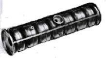
12 Exponential grow from middle 80 Multi-cell, β = 1, cavities for large storage rings KEK/TRISTAN (from 1987 to 1989) 200 MV peak RF voltage to the beam per revolution 32 x 5-cell 508 MHz DESY/HERA (from 1991 to 1993) 75/30 MV peak RF voltage to the electron beam One string of 16 x 4-cell 500 MHz CERN/LEP II (SC upgrade from 1996 to 2000) > 3.65 GV peak RF voltage to the beam per revolution 288 x 4-cell MHz (256 Sputtered) Multi-cell, β = 1, cavities for recirculating linacs TJNAF/CEBAF (from 1995 to 1999) 600 MV RF voltage to beam per linac pass 338 x 5-cell 1497 MHz RF Carlo Pagani 12

13 CEBAF and LEP II CEBAF 338 bulk niobium cavities Produced by industry Processed at TJNAF in a dedicated infrastructure 5-cell cavities 1.5 GHz, L act =0.5 m 4-cell cavities 352 MHz, Lact=1.7 m LEP II & CERN 32 bulk niobium cavities Limited to 5 MV/m Poor material and inclusions 256 sputtered cavities Magnetron-sputtering of Nb on Cu Completely done by industry Field improved with time <E acc > = 7.8 MV/m (Cryo-limited) Carlo Pagani 13


14 Large project impact on SRF technology The decision of applying this unusual technology in the largest HEP and NP accelerators forced the labs to invest in Research & Development, infrastructures and quality control The experience of industry in high quality productions has been taken as a guideline by the committed labs At that time TJNAF and CERN played the major role in SRF development, mainly because of the project size The need of building hundreds of cavities pushed the labs to transfer to Industry a large part of the production The large installations driven by HEP and NP produced a jump in the field R&D and basic research on SRF had also a jump thanks to the work of many groups distributed worldwide CEBAF LEP Carlo Pagani 14

 Integration of cavity ancillaries That is New level on Quality Control Carlo")
15 Important technological steps Use of the best niobium (and copper) allowable in the market at the time Industrial fabrication of cavity components with high level quality control Assembly of cavity components by Industry via Electron Beam welding in clean vacuum Use of ultra pure water for all intermediate cleaning Use of close loop chemistry with all parameters specified and controlled Cavity completion in Class 100 Clean Room Final cleaning and drying (UV for bacteria and on line resistivity control) Integration of cavity ancillaries That is New level on Quality Control Carlo Pagani 15

16 A great success for CEBAF Processing and conditioning improve cavity performances, when not limited by material defects (hard quench) Field emission moves to higher field Accelerating Field improves with time 2 K operation very reliable and well understood All ancillaries perform quite well Maximum energy and beam current above the design values CEBAF performances limited by the installed cryo-power and RF-power Guns 8.1% RF 6.1% Mag 5.5% Sft 4.4% Cryo 2.8% Control Net 2.5% FSD Trips 2.1% Vacuum 1.4% Plant 1.4% Other 1.2% PSS 1.1% MPS 0.8% Diag 0.6% RAD 0.5% SRF 0.3% 0 Excellent reliability of SRF technology High availability for physics The only warm-up for Isabelle Hurricane Lost Time Totals June'97-May'01 RF Problems 1.5 % in FY 01 FSD Faults CEBAF 0.0 % in FY 01 SRF Carlo Pagani 16
17 A great success for LEP II Accelerating Field Evolution with time from G. Geschonke s Poster for the ITRP visit to DESY Number of cavities GeV 100 GeV 104 GeV 96 GeV: Mean Nb/Cu 6.1 MV/m design 100 GeV: 3500MV Mean Nb/Cu 6.9 MV/m 104 GeV: 3666MV Mean Nb/Cu 7.5 MV/m Final energy reach limited by allowable cryogenic power Accelerating field [MV/m] Carlo Pagani 17
18 Same lessons learned Bulk Niobium is preferred to push for gradient and quality factor Magnetron sputtering looks better in some cases (LHC) when beam current is more important than accelerating field Cryogenics systems are highly reliable and produced by industry SRF ancillaries can be designed to be as reliable as the one required by the Normal Conducting RF technology 2 K operation and SRF quality controls end to be key factors For high gradient, E acc, and high quality factor, Q, Niobium quality has to be pushed to the possible limit Quality control during cavity production and surface processing has to be further improved. High Pressure Rinsing can make the difference Basic R&D and technological solutions must move together When fabrication procedures are fully understood and documented, Industry can do as well and possibly better Carlo Pagani 18
19 The TESLA Mission Develop SRF Technology for the future Linear Collider Basic goals on SRF Technology Increase gradient by a factor of 5: from 5 to 25 MV/m (Physical magnetic field limit for Nb is ~ 180 mt) Push cavity performances close to the physical limit, understanding practical limits Set all the required quality control for reproducibility and industrial production Make possible pulsed operation: Lorentz force detuning Combine SRF and mechanical engineering in cavity design Develop efficient Modulators and Klystrons Develop slow and fast tuners Develop appropriate couplers Reduce cost per MV by a factor 20: to make the LC feasible New cryomodule concept for cryolosses, cost and filling factor (for real estate gradient) All subsystems designed for large scale production Reliability and quality control as a general guide line Basic goals on Machine Design Design a Linear Collider based on the Cold Linac peculiarities Maximize Luminosity and optimize cost for a given plug power Design and quote major subsystems: DR, Positron Source, BDS, etc. Put all together in a consistent TDR, including cost estimation Carlo Pagani 19

 Hz/(MV/m) 2 - Niobium sheets (RRR=300) are scanned by eddy-currents to detect avoid foreign material inclusions like tantalum and iron - Industrial")
 from niobium sheets - Chemical preparation for welding, cleanroom preparation - Electron-beam welding according to detailed specification - 800 C high temperature heat treatment to")
20 Optimized Cavity Design and Rules Major contributions from: CERN, Cornell, DESY, CEA-Saclay & LASA Bulk Nb, 9-cell, 1.3 GHz Figure: Eddy-current scanning system for niobium sheets Figure: Cleanroom handling of niobium cavities R/Q TESLA cavity parameters E peak /E acc B peak /E acc Δf/Δl K Lorentz khz/mm Ω mt/(mv/m) Hz/(MV/m) 2 - Niobium sheets (RRR=300) are scanned by eddy-currents to detect avoid foreign material inclusions like tantalum and iron - Industrial production of full nine-cell cavities: - Deep-drawing of subunits (half-cells, etc. ) from niobium sheets - Chemical preparation for welding, cleanroom preparation - Electron-beam welding according to detailed specification C high temperature heat treatment to stress anneal the Nb and to remove hydrogen from the Nb C high temperature heat treatment with titanium getter layer to increase the thermal conductivity (RRR=500) - Cleanroom handling: - Chemical etching to remove damage layer and titanium getter layer - High pressure water rinsing as final treatment to avoid particle contamination Carlo Pagani 20


21 Eddy Current Scanner for Nb Sheets Scanning results Rolling marks and defects are visible on a niobium disk to be used to print a cavity half-cell. Surface analysis is then required to identify the inclusions Carlo Pagani 21


22 Cavity Production: EB welding and QC Carlo Pagani 22


23 Chemistry, HPR and String Assembly Carlo Pagani 23

24 HPWR crucial to cure Field Emission Field emission is normally caused by foreign particle contamination Emitted electron current grows exponentially with field Reaching the surface accelerated electrons produce cryo-losses and quenches Part of the electrons reaches high energies: Dark Current Particle causing field emission Temperature map of a field emitter Simulation of electron trajectories in a cavity Pictures taken from: H. Padamsee, Supercond. Sci. Technol., 14 (2001), R28 R51 Carlo Pagani 24


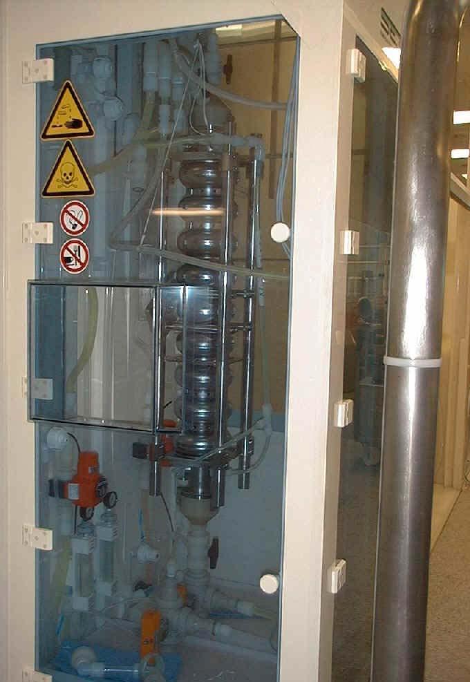
25 TTF: a new infrastructure at DESY TTF as operated for SASE FEL Carlo Pagani 25

26 Learning curve with BCP BCP = Buffered Chemical Polishing 3 cavity productions from 4 European industries: Accel, Cerca, Dornier, Zanon Cornell 1995 <E acc Q <E acc Q at Q = few 10 9 <2001> <1999> <1997> 5-cell Improved welding Niobium quality control Module performance in the TTF LINAC Carlo Pagani 26
27 3 rd cavity production with BCP 1E+11 1E+10 Q Still some field 3rd emission Production at high field- BCP Cavities Q-drop above 20 MV/m not cured yet Just AC67 discarded (cold He leak) TESLA original goal Q-drop AC55 AC57 AC59 AC61 AC63 AC65 AC67 AC69 AC56 AC58 AC60 AC62 AC64 AC66 AC68 AC79 1E Vertical CW tests of naked cavitis E acc [MV/m] Carlo Pagani 27
28 Two major contributions for high field In-Situ Baking ( C) from CEA-Saclay Cures Q-drop at High Field Formation of a uniform Nb 2 O 5, dielectric, layer on the surface Reduction of the normal conducting dissipation from NbO and NbO 2 Diffusion of the oxygen from the superconducting layer Some effect at the grain boundaries? Electro-polishing (EP) from KEK Improves field emission onset and maximum field Much smoother surface, less local field enhancement Better cleaning with high pressure water rinsing Foreign particles better removed High temperature (1400 C) heat treatment possibly avoidable Carlo Pagani 28
29 In-situ Baking effect 1,00E+11 Thermal breakdown 1,00E+10 Q 0 Strong degradation of the quality factor - No field emission! 1,00E+09 Electropolishing + after 120 C in-situ baking Power limit of the amplifier 1,00E E acc [MV/m] Carlo Pagani 29


30 Electro-Polishing for 35 MV/m Coordinated R&D effort: DESY, KEK, CERN and Saclay Nb sheet as delivered Main difference between BCP and EP: smoothening of grain boundaries. After 120 µm of BCP After120 µm of EP Carlo Pagani 30
31 EP & Baking for 35 MV/m The AC 70 example EP at the DESY plant Low Field Emission Vertical and System Test in 1/8th Cryomodule 800 C annealing 120 C, 24 h, Baking high field Q drop cured High Pressure Water Rinsing Few nω residual resistance Negligible Field Emission Electro-Polishing (EP) instead of Buffered Chemical Polishing (BCP) less local field enhancement High Pressure Rinsing more effective Field Emission onset at higher field In Situ C for hours to re-distribute oxygen at the surface cures Q drop at high field Carlo Pagani 31
32 Field Emission pushed to higher field BCP Cavities used in Modules 4 & 5 are in red, EP cavities in blue Radiation Dose from the fully equipped cavities while High Power Tested in Chechia Chechia is the horizontal cryostat equivalent to 1/8 of a TTF Module BCP E acc = 25 MV/m Radiation dose producing 50 na of captured Dark Current: that is the TESLA safe limit giving 200 mw of induced cryo-losses at 2 K BCP = Buffered Chemical Polishing EP = Electro-Polishing EP E acc = 35 MV/m Carlo Pagani 32
33 TESLA Cavities: all tests to June 05 Taking into account all data from Emax FE start E surf [MV/m] /1/1995 1/1/1997 1/1/1999 1/1/2001 1/1/2003 1/1/2005 Carlo Pagani 33
34 ILC is now driving SRF R&D Main Linacs are the biggest single cost item for ILC 10 years of R&D by the TESLA collaboration has produced a fantastic technology: a great proof of existence But we re not quite there yet Primary focus of the SRF R&D driven by ILC: Define/understand the QC & QA parameters for high performance Perform a coordinate engineering effort on major components Technology transfer to several industries through prototypes Cost reduction and reliability through guided industrialisation Maintain within the Institutions the full awareness of the essential technologies: the LHC dipoles example should be followed XFEL project is already doing much within Europe New Test Facilities will work in a coordinate way Effort for maximum gradient is crucial for cost and reliability Carlo Pagani 34

 Gradient MV/m Cornell and JLab are also testing low B geometries Carlo")
35 ILC Gradient and the R&D on Shapes Relative Cost 35MV/m is close to optimum 30 MV/m would give safety margin a + b G $ lin cryo G Q 2 0 KEK is pushing for 40-45MV/m ICHIRO cavity Larger magnetic volume: Lower peak magnetic field Lower cryogenic losses But: higher field emission? C. Adolphsen (SLAC) Gradient MV/m Cornell and JLab are also testing low B geometries Carlo Pagani 35

 As received After 800 C annealing Crystal grains change with the 800 C heat treatment for dehydrogenization and stress release Carlo Pagani 36")
36 JLab is driving an essential R&D on Nb Niobium quality remains the major issue to completely understand and define Quality Control & Quality Assurance parameters Most of the niobium cost is determined by the effort of preserving quality through casting rolling and heat treatments required for homogenous grain and reasonable isotropy Many producer could deliver pure Nb at the ingot state but few can supply sheets with the required minimal properties QC & QA are very difficult and expensive Microstructure is Heterogeneous (Banded) As received After 800 C annealing Crystal grains change with the 800 C heat treatment for dehydrogenization and stress release Carlo Pagani 36
 140 120 100 80 60 40 20 K P Grain size grow and orientation depend from the batch used and varies from sheet to sheet of the same batch Define QC")
37 Grain Problems in nowadays Niobium Niobium sheet cut after the 800 annealing. Colors refers to crystal orientations Grain size (μm) K P Grain size grow and orientation depend from the batch used and varies from sheet to sheet of the same batch Define QC and QA for the required mechanical properties is a concern Cavity shape and treatment results are effected by this heterogeneity, grain boundaries and their orientation 0 20' 600' 700' 750' 800' Temperture (C) Inclusions or clusters in the bulk at the several μm level are not detectable Carlo Pagani 37

38 Large or Single Crystals are promising Peter Kneisel at JLab is leading a collaboration that try to qualify niobium sheets obtained by EDM (Electron Discharge Machining) directly from the ingot Preliminary results are very promising In case of success, material QC and QA would be much easier and the cost much cheaper 2.2 GHz Single crystal single cell cavity Q 0 vs. B p ~ 80 micron BCP 1:1:2 1.0E+11 T=2K, after 120C 48h bake T=1.5K after 120C 48h bake T=2K T=1.5K Theoretical limit reached Q 0 1.0E+10 Field emission, after baking Q-drop P. Kneisel pulsed RMS Surface Roughness 27 nm 1.0E B p [mt] Carlo Pagani 38
39 Some Lessons and Hopes The presently used high RRR niobium properties appear to be not consistent from batch to batch, from sheet to sheet and even from different sheet locations Single crystal niobium discs sliced directly from the ingots can be expected to have consistent properties from batch to batch, while being less expensive. high fields close to the fundamental limit have been reached; Extrapolation to the ILC_LL shape at 1.3 GHz gives E acc ~51 MV/m, at Q 0 = 1.5x10 10 Q- drop shifted to higher gradients but still present and most likely not due to grain boundaries very low ( ~1 nω) residual resistance, because of missing grain boundaries? Material with high Ta contents (~ 800 ppm) gives good results BCP is very well a feasible process to achieve high performance and could potentially replace EP 1000 Thermal Conductivity (W/mK) 100 Thermal Conductivity Peak observed Single Crystal Heat Treated Poly Crystal Poly Crystal Heat Treated at 1250 C Two Crystals G. Rao Myneni Temperature (K) Margin for He bath temperature optimization? Carlo Pagani 39