Lattice 3256A-90LM PLD
|
|
|
- Allan George
- 5 years ago
- Views:
Transcription
1 Construction Analysis PLD Report Number: SCA Global Semiconductor Industry the Serving Since N. Hartford Drive Scottsdale, AZ Phone: Fax: Internet:
2 INDEX TO TEXT TITLE PAGE INTRODUCTION 1 MAJOR FINDINGS 1 TECHNOLOGY DESCRIPTION Die Process 2 ANALYSIS RESULTS I Die Process and Design 3-5 ANALYSIS PROCEDURE 6 TABLES Overall Quality Evaluation 7 Die Material Analysis (EDX) 8 Horizontal Dimensions 9 Vertical Dimensions 10 - i -
3 INTRODUCTION This report describes a construction analysis of the Programmable Logic Device (PLD). One decapped device was received for the analysis. The device was date coded MAJOR FINDINGS Questionable Items: 1 Aluminum 1 thinning up to 100 percent 2 (Figure 15). Total metal 1 thinning was reduced to 90 percent with the addition of the cap and barrier. Special Features: Sub-micron gate lengths (0.5 micron N-channel and 0.6 micron P-channel). Design Features: Slotted and beveled metal 2 bus lines. 1 These items present possible quality or reliability concerns. They should be discussed with the manufacturer to determine their possible impact on the intended application. 2 Seriousness depends on design margins
4 TECHNOLOGY DESCRIPTION Die Process and Design: The device was fabricated using a selective oxidation, twin-well CMOS process in a P-substrate. No epi was used. Passivation consisted of a layer of nitride over a layer of silicon-dioxide. Metallization employed two levels of metal. Both consisted of aluminum with a titanium-nitride (TiN) cap and barrier. A thin titanium (Ti) adhesion layer was used under metal 1. Standard vias and contacts were used (no plugs). The interlevel dielectric consisted of two layers of glass with a spin-on-glass (SOG) between the two layers. Pre-metal glass consisted of a layer of reflow glass over various densified oxides. Glass was reflowed prior to contact cuts only. A single layer of polycide (tungsten silicide) was used to form one plate of the capacitors and all gates on the die. Direct poly-to-diffusion (buried) contacts were not used. Definition was by a dry etch of normal quality. Standard implanted N+ and P+ diffusions formed the sources/drains of the CMOS transistors. An LDD process was used with oxide sidewall spacers left in place. Local oxide (LOCOS) isolation. A step was present at the edge of the well which indicates a twin-well process was used. No problems were noted. Two EEPROM cell arrays were used on the device. Both devices are programmed through an ultra thin (tunnel) oxide window. Metal 2 was used to form the bit lines and distribute ground on array B. Metal 1 was used for interconnect and to distribute ground on array A. Poly was used to form the gates and one plate of the capacitors and gates
5 ANALYSIS RESULTS I Die Process : Figures 1-36 Questionable Items: 1 Aluminum 1 thinning up to 100 percent 2 (Figure 15). Total metal 1 thinning was reduced to 90 percent with the addition of the cap and barrier. Special Features: Sub-micron gate lengths (0.5 micron N-channel and 0.6 micron P-channel). Design features: Slotted and beveled metal 2 bus lines. General items: Fabrication process: Devices were fabricated using a selective oxidation, twin-well CMOS process in a P-substrate. No epi was used. Process implementation: Die layout was clean and efficient. Alignment was good at all levels. No damage of contamination was found. Die coat: No die coat was present. Overlay passivation: A layer of nitride over a layer of silicon-dioxide. Overlay integrity test indicated defect-free passivation. Edge seal was good. 1 These items present possible quality or reliability concerns. They should be discussed with the manufacturer to determine their possible impact on the intended application. 2 Seriousness depends on design margins
6 ANALYSIS RESULTS I (continued) Metallization: Two levels of metal. Both consisted of aluminum with titaniumnitride (TiN) caps and barriers. A thin titanium (Ti) adhesion layer was present beneath metal 1. Standard vias and contacts were used (no plugs). Metal patterning: Both metal levels were patterned by a dry etch of normal quality. Metal defects: No voiding, notching, or neckdown was noted in the metal of either layer. Contacts and vias were completely surrounded by metal. No silicon nodules were noted following removal of either metal layer. Metal step coverage: Metal 2 aluminum thinned up to 75 percent at vias. Total metal 2 thinning was reduced to 65 percent with the addition of the cap and barrier. Metal 1 aluminum thinned up to 100 percent at some contacts. Total metal 1 thinning was reduced to 90 percent with the addition of the cap and barrier. Interlevel dielectric: Two layers of silicon-dioxide were present under metal 2 (interlevel dielectric). The first layer had been subjected to an etchback process. A layer of spin-on-glass (SOG) was present between the layers for planarization purposes. Pre-metal glass: A layer of reflow glass over various densified oxides was used under metal 1. Reflow was performed prior to contact cuts only. No problems were found. Contact defects: Contact and via cuts were defined by a two-step process. No over-etching of the contacts or vias was noted. A single layer of polycide (tungsten silicide) was used to form all gates on the die and one plate of the capacitors. Direct poly-to-diffusion (buried) contacts were not used. Definition was by a dry-etch of normal quality
7 ANALYSIS RESULTS I (continued) Standard implanted N+ and P+ diffusions formed the sources/drains of the CMOS transistors. An LDD process was used with oxide sidewall spacers left in place. No problems were found. Local oxide (LOCOS) isolation was used with a step present at the well boundary indicating that a twin-well process was employed. Two EEPROM cell arrays were used on the device. Both use the same design (but different layout) and are programmed through an ultra thin (tunnel) oxide window. Metal 2 was used to form the bit lines and distribute ground on array B. Metal 1 was used for interconnect and to distribute ground in array A. Poly was used to form the gates and one plate of the capacitors. Cell size (array A): 9.0 x 9.5 microns. Cell size (array B): 13 x 36 microns Redundancy fuses were not present on the die
8 PROCEDURE The devices were subjected to the following analysis procedures: Internal optical inspection SEM of passivation Passivation integrity test Passivation removal SEM inspection of metal 2 Metal 2 removal and inspect barrier Delayer to metal 1 and inspect Metal 1 removal and inspect barrier Delayer to silicon and inspect poly/die surface Die sectioning (90 for SEM) * Die material analysis Measure horizontal dimensions Measure vertical dimensions * Delineation of cross-sections is by silicon etch unless otherwise indicated
9 OVERALL QUALITY EVALUATION : Overall Rating: Normal DETAIL OF EVALUATION Die surface integrity: Toolmarks (absence) Particles (absence) Contamination (absence) Process defects General workmanship Passivation integrity Metal definition Metal integrity * Metal registration Contact coverage Contact registration G G G G N G N N N N N * Even with the isolated spots where metal 1 thins 100 percent we judge adequate metal remains around the contact perimeter. G = Good, P = Poor, N = Normal, NP = Normal/Poor - 7 -
10 DIE MATERIAL ANALYSIS Final passivation: A layer of silicon-nitride over a layer of glass. Metallization 2: Metallization 1: Silicide (poly): Aluminum (Al) with a titanium-nitride (TiN) cap and barrier. Aluminum (Al) with a titanium-nitride (TiN) cap and barrier on a thin titanium (Ti) adhesion layer. Tungsten (W)
11 HORIZONTAL DIMENSIONS Die size: 7.4 x 9.2 mm (290 x 364 mils) Die area: 68 mm 2 (105,560 mils 2 ) Min pad size: Min pad window: Min pad space: Min metal 2 width: Min metal 2 space: Min metal 2 pitch: Min metal 1 width: Min metal 1 space: Min metal 1 pitch: Min via: Min contact: Min polycide width: Min polycide space: Min gate length * - (N-channel): 0.1 x 0.1 mm (4.0 x 4.0 mils) 0.09 x 0.09 mm (3.8 x 3.8 mils) 28 microns 1.1 micron 1.1 micron 2.2 microns 0.8 micron 0.8 micron 1.6 micron 0.85 micron 0.8 micron 0.5 micron 0.7 micron 0.5 micron - (P-channel): 0.6 micron Cell pitch (array A): 9.0 x 9.5 microns Cell size (array A): 85.5 microns 2 Cell pitch (array B): 13 x 35 microns Cell size (array B): 455 microns 2 * Physical gate length - 9 -
12 VERTICAL DIMENSIONS Die thickness: 0.5 mm (20 mils) Layers: Passivation 2: 0.45 micron Passivation 1: 0.25 micron Metal 2 - cap: 0.05 micron (approximate) - aluminum: 0.8 micron - barrier: 0.12 micron Interlevel dielectric- glass 2: 0.4 micron - glass 1: 0.3 micron (average) Metal 1 - cap: 0.07 micron (approximate) - aluminum: 0.5 micron - barrier: 0.12 micron Pre-metal dielectric: 0.75 micron (average) Oxide on polycide: 0.15 micron Polycide - silicide: 0.1 micron - poly: 0.12 micron Local oxide: 0.45 micron N+ S/D: 0.13 micron P+ S/D: 0.2 micron N-well: 4.0 microns P-well: 4.0 microns
13 INDEX TO FIGURES DIE LAYOUT AND IDENTIFICATION Figures 1-3 PHYSICAL DIE STRUCTURES Figures 4-39 COLOR DRAWING OF DIE STRUCTURE Figure 21 EEPROM CELL (ARRAY A) Figures EEPROM CELL (ARRAY B) Figures INPUT PROTECTION CIRCUIT Figure 36 GENERAL CIRCUIT LAYOUT Figure 36 - ii -

14 Figure 1. Whole die photograph of the. Mag. 25x.

15 Figure 2. Markings from the die surface. Mag. 320x.


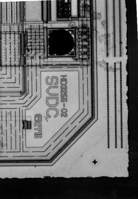
16 Figure 3. Optical views of the die corners on the. Mag. 160x.


17 Mag. 170x Mag. 600x Figure 4. Perspective SEM views of dicing and edge seal. 60.


18 DIE EDGE Mag. 1400x METAL 1 METAL 2 Mag. 3200x METAL 2 METAL 1 Mag. 6500x Figure 5. SEM section views of the edge seal.


19 METAL 2 POLY INTERLEVEL DIELECTRIC METAL 1 N+ S/D METAL 2 METAL 1 N+ S/D Figure 6. SEM section views of general device structure. Mag. 10,000x.


20 Mag. 5200x Mag. 10,000x Figure 7. Perspective SEM views of overlay passivation coverage. 60.


21 PASSIVATION METAL 2 INTERLEVEL DIELECTRIC METAL 1 Mag. 13,000x PASSIVATION 2 TiN CAP PASSIVATION 1 ALUMINUM 2 TiN BARRIER INTERLEVEL DIELECTRIC Mag. 26,000x Figure 8. SEM section views of metal 2 line profiles.


22 METAL 2 Mag. 2000x VIA METAL 2 Mag. 4000x Figure 9. Topological SEM views of metal 2 patterning.


23 METAL 2 Mag. 6500x METAL 2 Mag. 13,000x PASSIVATION Mag. 26,000x METAL 2 INTERLEVEL DIELECTRIC METAL 1 Figure 10. SEM views of metal 2 coverage and via.


24 INTERLEVEL DIELECTRIC ALUMINUM 1 PRE-METAL DIELECTRIC Mag. 40,000x TiN CAP SOG ALUMINUM 1 TiN BARRIER Mag. 52,000x Figure 11. SEM section views of metal 1 line profiles.


25 METAL 1 Mag. 3200x METAL 1 CONTACT Mag. 6500x Figure 12. Topological SEM views of metal 1 patterning. 0.


26 METAL 1 Mag. 6500x METAL 1 CONTACT Mag. 20,000x Figure 13. Perspective SEM views of metal 1 coverage. 60.


27 TiN BARRIER 60 SOG PRE-METAL DIELECTRIC METAL 1 POLY glass etch Figure 14. SEM views of barrier coverage and a metal contact. Mag. 26,000x.


28 100% THINNING PRE-METAL DIELECTRIC metal 1-to-P+ METAL 1 POLY P+ S/D P+ S/D SOG PRE-METAL DIELECTRIC metal 1-to-N+ METAL 1 POLY N+ S/D N+ S/D INTERLEVEL DIELECTRIC SOG METAL 1 metal 1-to-poly PRE-METAL DIELECTRIC POLY Figure 15. SEM section views of typical metal 1 contacts. Mag. 26,000x.


29 N+ P+ POLY Mag. 3200x POLY Mag. 6500x Figure 16. Topological SEM views of poly patterning. 0.


30 Mag. 6500x POLY POLY Mag. 40,000x LOCAL OXIDE DIFFUSION Mag. 40,000x POLY LOCAL OXIDE DIFFUSION Figure 17. Perspective SEM views of poly coverage. 60.


31 PRE-METAL DIELECTRIC SIDEWALL SPACER POLY glass etch PRE-METAL DIELECTRIC POLY METAL 1 P-channel P+ S/D P+ S/D GATE OXIDE PRE-METAL DIELECTRIC N-channel N+ S/D N+ S/D GATE OXIDE Figure 18. SEM section views of typical transistors. Mag. 52,000x.


32 PRE-METAL DIELECTRIC LOCAL OXIDE POLY BIRDSBEAK Figure 19. SEM section view of a local oxide birdsbeak. Mag. 52,000x. LOCAL OXIDE Mag. 26,000x STEP Mag. 800x P-WELL N-WELL P-SUBSTRATE Figure 20. Section views of the well structure.
33 POLY,,,,,, INTERLEVEL DIELECTRIC,,,,,,,,,,,, SOG,,,,,,,,,,,, N+ S/D P-WELL LOCAL OXIDE METAL 1 METAL 2 PRE-METAL DIELECTRIC P+ S/D Orange = Nitride, Blue = Metal, Yellow = Oxide, Green = Poly, Red = Diffusion, and Gray = Substrate Figure 21. Color cross section drawing illustrating device structure. PASSIVATION 2 PASSIVATION 1,,,,,,,,,,,,,,,,,,,,,,,,,,,,,,,,,,,,,,,,,,,,,,,,,,,, N-WELL


34 metal 2 metal 1 poly Figure 22. Perspective SEM views of the EEPROM cell array. Array A, Mag. 3200x, 60.


35 Mag. 6500x TUNNEL OXIDE DEVICE Mag. 26,000x Figure 23. Detailed SEM views of the EEPROM cell array. Array A, 60.


36 metal 2 metal 1 poly Figure 24. SEM views of the EEPROM cell array. Array A, Mag. 1600x, 0.


37 BIT B metal 2 A BIT GND metal 1 Figure 25. Additional SEM views of the EEPROM cell array. Array A, Mag. 3200x,

38 2 C 1 poly WORD BIT 2 1 C B Figure 26. SEM view and schematic of the EEPROM cell. Array A, Mag. 3200x, 0.

39 TUNNEL OXIDE WINDOW Figure 27. Topological SEM view of the tunnel oxide window. Array A, Mag. 13,000x, 0.


40 METAL 1 Mag. 13,000x SELECT GATE TUNNEL OXIDE DEVICE POLY GATE PRE-METAL DIELECTRIC Mag. 40,000x POLY SELECT GATE N+ S/D N+ S/D POLY Mag. 52,000x N+ S/D N+ S/D GATE OXIDE TUNNEL OXIDE Figure 28. SEM section views of an EEPROM cell. Array A.


41 metal 2 metal 1 poly Figure 29. Perspective SEM views of the additional EEPROM cell array. Array B, Mag. 1600x, 60.


42 metal 2 metal 1 poly Figure 30. SEM views of additional EEPROM cells. Array B, Mag. 1600x.


43 BIT 0 GND A metal 2 B BIT 1 metal 1 Figure 31. Detailed SEM views of additional EEPROM cell. Array B, Mag. 3200x. 0.

44 WORD C poly BIT 0 C1 1 A 3 WORD 2 B BIT 1 Figure 32. Detailed SEM view and schematic of additional EEPROM cell. Array B, Mag. 3200x, 0.


45 METAL 2 METAL 1 SELECT GATE TUNNEL OXIDE DEVICE POLY GATE Mag. 10,000x POLY N+ S/D N+ S/D TUNNEL OXIDE Mag. 40,000x Figure 33. SEM section views of additional EEPROM cell. Array B.


46 METAL 1 Mag. 5000x TUNNEL OXIDE DEVICE CAPACITOR PRE-METAL DIELECTRIC POLY Mag. 37,000x N+ TUNNEL OXIDE POLY Mag. 52,000x N+ TUNNEL OXIDE Figure 34. SEM section views of additional EEPROM cell. Array B.


47 METAL 1 CAPACITORS Mag. 8000x POLY CAPACITOR Mag. 20,000x Figure 35. SEM section views of additional EEPROM cell through the capacitor region. Array B.


48 Mag. 320x Mag. 800x Figure 36. Optical views of an I/O structure and general circuitry.