Influence of the acid and alkaline texturization process on basic opto-electronic parameters of the silicon solar cells
|
|
|
- Stuart Doyle
- 5 years ago
- Views:
Transcription

1 Influence of the acid and alkaline texturization process on basic opto-electronic parameters of the silicon solar cells GraŜyna Kulesza M.Sc. Supervisor: Prof. Paweł Zięba, Ph.D., D.Sc. Secondary Supervisor: Piotr Panek Ph.D. Institute of Metallurgy and Materials Science PAS, 25 Reymonta Str., Krakow, Poland Photovoltaic Laboratory, 22 Krakowska Str., Kozy


2 Texturization the aim of process Alkaline texturization of monocrystalline silicon Acid texturization of polycrystalline silicon Samples prepared for SEM investigations Pyramidal structures after alkaline texturization Rounded pits structures after acid texturization 100 % 100 % 11 % 11 % 33 % o θ X TEX 33 % 67 % 22% 67 % 22% (100) Oriented back Si surface

 Another cleaning technology : 2% HF -1 min CHCl-CCl 2 -rinsing CH 3 -CO-CH 3")

 Temperature - ambient time: 15-180 sec Acid")
3 Preliminary etching : 30% KOH, 80 C, 3 min KOH:IPA:DIW (1:3:46) 80 C (40 min) KOH:DAA:DIW C (10; 15; 17.5; 20; 30; 40 min) KOH:1,2-pentanediol:DIW (1M KOH, 2% alcohol) C, min, with and without blending) Another cleaning technology : 2% HF -1 min CHCl-CCl 2 -rinsing CH 3 -CO-CH 3 hot -rinsing H 2 SO 4 :DIW (1:1) -etching DIW -rinsing HF:DIW (1:10) - etching DIW -rinsing Texturization the mixture preparation Alkaline texturization T b H 2 O = 100 C T b CH 3 CH(OH)CH 3 = 82 C T b CH 3 CH(O)CH 2 C(CH 3 )(OH)CH 3 = 158 C T b CH 2 (OH)CH(OH)CH 2 CH 2 CH 3 = 206 C HF:HNO 3 :diluent (CH 3 COOH or DIW) Temperature - ambient time: sec Acid texturization Cz-Si before and after texturization process mc-si before and after texturization process


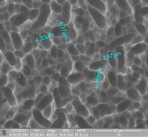
4 SEM measurements FEI E-SEM XL30; FEI QUANTA 200 3D Dual Beam; Hitachi SU µm 10 µm 20 µm defected surface after diamond saw cutting 20 µm surface after KOH preliminary etching 20 µm surface after main alkaline texturization 10 µm 10 µm


5 SEM measurements FEI E-SEM XL30; FEI QUANTA 200 3D Dual Beam; 20 µm 20 µm 7 HF : 1 HNO 3 : 2 CH 3 COOH 7 HF : 1 HNO 3 : 2 H 2 O 20 µm 20 µm 20 µm 20 µm 1 HF : 7 HNO 3 : 2 CH 3 COOH 1 HF : 7 HNO 3 : 2 H 2 O 7 HF : 1 HNO 3 : 2 H 2 O 20 µm 20 µm 20 µm 20 µm 0 sec 30 sec 45 sec 60 sec
6 Reflectance measurements Ocean Optics QE spectrometer with integrated light source DH-2000-BALL R [%] Cz-Si etched (KOH) Cz-Si grinded Cz-Si txtured (KOH:IPA:DIW) Cz-Si with AR coating (TiO 2 ) λ [nm] R [%] mc-si grinded mc-si textured (KOH:IPA:DIW) mc-si etched (KOH) mc-si with AR coating (TiO 2 ) λ [nm] Texturization in alkaline solutions reduces the reflectance of monocrystalline silicon up to 10 % but is ineffective for polycrystalline silicon there is no significant reflectance reduction after texturization process.
7 Reflectance measurements Ocean Optics QE spectrometer with integrated light source DH-2000-BALL HNO 3 CH 3 COOH (60 s) CH 3 COOH (180 s) H 2 O (60 s) HF CH 3 COOH (60 s) H 2 O (60 s) H 2 O (120 s) Ref HNO 3 CH 3 CO OH (12 0 se c) C H 3 C OO H (180 sec) H 2 O (120 sec) HF CH 3 CO OH (12 0 se c) H 2 O (60 sec) H 2 O (120 sec) R [%] R [%] λ [nm] λ [nm] Texturization in acid solutions reduces the reflectance of polycrystalline silicon up to 10 % in mixtures with high HF content with deionized wateras a diluent. Additionally the shortest process time (60 seconds) was the bestone. This is due to the larger surface roughness after wafers texturization in high HF content solution as shown by the AFM investigations in the following slide.

8 AFM, profilometer measurements AFM: Park Systems XE-100 Profilometer: Taylor Hobson Surtronic 25 Ra = 1.13 Rq = HF:1HNO 3 :1H 2 O 8HF:1HNO 3 :1H 2 O 1HF:8HNO 3 :1H 2 O Ra = Rq = HF:8HNO 3 :1H 2 O Profilometer investigations shows larger roughness for texturing in high HF content solutions. Line Min Max Mid Mean Rq Ra Line Min Max Mid Mean Rq Ra Red Green Red Green More precise from profilometer studies are AFM investigations. Again the larger roughness of texturing wafers in the high HF content solutions is observed.


9 Wettability measurements Attension optical tensiometer Theta Lite A B C 8HF:1HNO 3 :1H 2 O 1HF:8HNO 3 :1H 2 O 1HF:8HNO 3 :1CH 3 COOH D Sample number Mean Contact angle [degrees] Standard deviation [degrees] Mean Volume [microl] Standard deviation [microl] A 134,84 1,39 13,41 0,11 B 46,43 2,83 16,73 10,70 C 85,74 16,63 17,68 11,43 D 38,39 3,24 9,07 1,69 8HF:1HNO 3 :1CH 3 COOH Wafers texturing in high HF content solutions with deionized water as a diluent shows hydrophobic properties. Therefore it is necessary to rinse the wafers with isopropyl alcohol at elevated temperatures.
 phosphorous silica glass PSG removal using 10% HF passivation by thermal oxidation")
 characteristics examination: LIV simulator calibrated by the reference cell measured at the Institut für Solarenergieforshung GmbH Hameln/Emmerthal (AM 1.")
![5, 1000 W/m 2, 25 C) Type of silicon Type of texturing mixture Temperature and time I SC [ma] V OC [mv] P m [mw] FF [%] Eff [%} Cz-Si KOH:DAA:DIW 1 :3 : 46 94-96 C 10 min 845.7 592.6 385.9 77.](/docs-images/95/125309399/images/10-3.jpg "0 15.4 mc-si HF:HNO 3 :DIW 7 : 1 : 2 ambient 60 sec 769.2 583.3 340.4 75.9 13.")
10 Solar cells manufacturing process: p-n junction formation by diffusion from POCl 3 as a source at temperature 850 C for 25 min (20 min prediffusion and 5 min re-diffusion) resulting in the surface resistance R s = 53 Ω/ edge separation (CP-4 mixture: 3 HF : 5 HNO 3 : 3 CH 3 COOH in volume ratio) phosphorous silica glass PSG removal using 10% HF passivation by thermal oxidation at 800 C for 10 min antireflective coating deposition of TiO x by CVD method screen-printing ohmic contacts using Ag and Al pastes (Du Pont PV 159, PV 381) firing in III-zone belt IR furnace Light current-voltage (LIV) characteristics examination: LIV simulator calibrated by the reference cell measured at the Institut für Solarenergieforshung GmbH Hameln/Emmerthal (AM 1.5, 1000 W/m 2, 25 C) Type of silicon Type of texturing mixture Temperature and time I SC [ma] V OC [mv] P m [mw] FF [%] Eff [%} Cz-Si KOH:DAA:DIW 1 :3 : C 10 min mc-si HF:HNO 3 :DIW 7 : 1 : 2 ambient 60 sec I sc short circuit current, V oc open circuit voltage, P m maximum power, FF fill factor, E ff photovoltaic conversion efficiency
11 Future investigations: Upcoming researches: Silicon defects designation for raw material and silicon wafers after texturization process (cooperation with Institute of Physics, Wrocław University of Technology) Carrier lifetime (for the characterization of a good texture) Influence of texturization process temperature on opto-electronic parameters of silicon wafers and solar cells investigations (temperature lowering, cooling medium) Further researches: Determine the area of dislocation etching on the concentration triangle in order to avoid this type of solution (wafers fragility) Determination of the formation of porous silicon Surface development investigations: mercury porosimetry or nitrogen sorption (cooperation with Faculty of Materials Engineering and Ceramics, AGH University of Technology) Determination of recombination centers by LBIC (Light Beam Inducted Current) Determination of IQE (Internal Quantum Efficiency)