Physics and Material Science of Semiconductor Nanostructures
|
|
|
- Phebe Allen
- 5 years ago
- Views:
Transcription
1 Physics and Material Science of Semiconductor Nanostructures PHYS 570P Prof. Oana Malis
2 Today Bulk semiconductor growth Single crystal techniques Nanostructure fabrication Epitaxial growth MBE Ref. Ihn Chapter 2
3 Types of Crystalline Semiconductors: Silicon Different levels of crystal structure may exist ranging from single crystal to totally non-crystalline Single crystal silicon Multi-crystal silicon Polycrystalline Ribbon silicon Amorphous silicon The main difference between each is the crystal grain size and their growth technique
4 Different Forms of Silicon Crystal Type Symbol Crystal Grain Size Common Growth Techniques Single-crystal sc-si > 10 cm Czochralski (Cz), Float-Zone (FZ) Multicrystalline mc-si 10cm Cast, Spheral, Sheet, ribbon Polycrystalline pc-si 1 m 1mm Evaporation, CVD, sputtering
5 Crystal growth Process flow from starting material to polished wafer.
6 Semiconductor-Grade Silicon Steps to Obtaining Semiconductor Grade Silicon (SGS) Step Description of Process Reaction Reduction of silica: produce metallurgical grade silicon (MGS) by heating silica with carbon (97% pure) Purify MG silicon through a chemical reaction to produce a silicon-bearing gas of trichlorosilane (SiHCl 3 ) Additional purification via distillation CVD: SiHCl 3 and hydrogen react in a process called Siemens to obtain pure semiconductor- grade silicon (SGS) SiC (s) + SiO 2 (s) Si (l) + SiO(g) + CO (g) Si (s) + 3HCl (g) SiHCl 3 (g) + H 2 (g) + heat 2SiHCl 3 (g) + 2H 2 (g) 2Si (s) + 6HCl (g)
7 Single Crystal Growth Techniques Czochralski Growth (Cz) Most single crystal silicon made this way Lower quality silicon than FZ with Carbon and Oxygen present Cheaper production than FZ Produces cylinders and circular wafers Float Zone (FZ) Better Quality than Cz More Expensive than Cz Produces cylinders and circular wafers
 The melt temperature, rotation rate and pull rate are controlled to create an ingot of a certain")
8 Czochralski Method Pure Silicon is melted in a quartz crucible under vacuum or inert gas and a seed crystal is dipped into the melt The seed crystal is slowly withdrawn and slowly rotated so that the molten silicon crystallizes to the seed (Rock Candy) The melt temperature, rotation rate and pull rate are controlled to create an ingot of a certain diameter


9 Modern CZ Crystal Growth The raw Si used for crystal growth is purified from SiO 2 (sand) through refining, fractional distillation and CVD. The raw material contains < 0.01 ppb impurities except for O ( cm -3 ) and C ( cm -3 ) Essentially all Si wafers used for ICs today come from Czochralski grown crystals. Polysilicon material is melted, held at close to 1415 C, and a single crystal seed is used to start the crystal growth. Pull rate, melt temperature and rotation rate are all important control parameters.
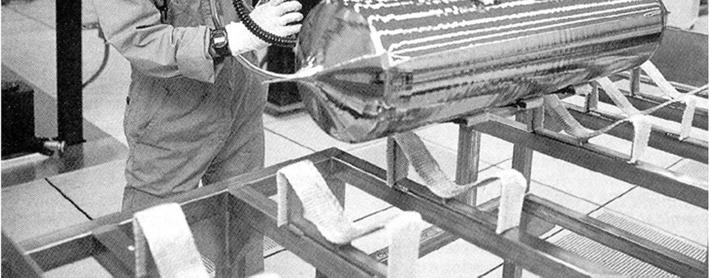
10 Czochralski Technique Spinning rod with Seed Crystal lowered into the molten silicon Slowly pulled up to allow silicon to crystallize on the seed layer Molten Silicon Once to the size desired, the crystal is pulled faster to maintain the needed diameter

11 CZ crystal growth (cont.) Sequence of photographs and drawings illustrating CZ crystal growth. The charge is melted, the seed is inserted, the neck region is grown at a high rate to remove dislocations and finally the growth is slowed down to produce a uniform crystal.

12 Czochralski Growth Entire ingots of silicon produced as one big crystal Very high quality material with few defects No boundaries between crystals because it is one crystal in one orientation Si crystal inevitably contains oxygen impurities dissolved from the quartz crucible holding the molten silicon 13
 Boule")
13 12 (30 cm) Boule

14 Drawback of the CZ method The only significant drawback to the CZ method is that the silicon is contained in liquid form in a crucible during growth and as a result, impurities from the crucible are incorporated in the growing crystal. Oxygen and carbon are the two most significant contaminants. These impurities are not always a drawback, however. Oxygen in particular can be very useful in mechanically strengthening the silicon crystal and in providing a means for gettering other unwanted impurities during device fabrication. Lacture # 3 15

15 Float Zone Method Produced by cylindrical polysilicon rod that already has a seed crystal in its lower end An encircling inductive heating coil melts the silicon material The coil heater starts from the bottom and is raised pulling up the molten zone A solidified single crystal ingot forms below Impurities prefer to remain in the molten silicon so very few defects and impurities remain in the forming crystal
16 Dopant Concentration Nomenclature Dopant Material Type < (Very Lightly Doped) Concentration (Atoms/cm 3 ) to (Lightly Doped) to (Doped) >10 19 (Heavily Doped) Pentavalent n n -- n - n n + Trivalent p p -- p - p p +

17 Basic Process Steps for Wafer Preparation Crystal Growth Wafer Lapping and Edge Grind Cleaning Shaping Etching Inspection Wafer Slicing Polishing Packaging

18 Slicing into Wafers Ingots are cut into thin wafers Two Techniques Wire sawing Diamond blade sawing Both results in loss of silicon from kerf losses silicon saw dust Time consuming Water Cooled, Dirty


19 Ingot Diameter Grind Preparing crystal ingot for grinding Internal diameter wafer saw Diameter grind Flat grind


20 Wafer Polishing: single or double side Upper polishing pad Wafer Slurry Lower polishing pad


21 Wafer Notch and Laser Scribe Notch Scribed identification number Chemical Etch of Wafer Surface to Remove Sawing Damage
22 Silicon Wafer Fabrication Review Raw materials (SiO 2 ) are refined to produce electronic grade silicon with a purity unmatched by any other available material on earth. CZ crystal growth produces structurally perfect Si single crystals which are cut into wafers and polished. Starting wafers contain only dopants, and trace amounts of contaminants O and C in measurable quantities. Dopants can be incorporated during crystal growth Point, line, and volume (1D, 2D, and 3D) defects can be present in crystals, particularly after high temperature processing. Point defects are "fundamental" and their concentration depends on temperature (exponentially), on doping level and on other processes like ion implantation which can create non-equilibrium transient concentrations of these defects.
23 Nanostructure fabrication


24 Top-down versus bottom up: An analogy If we want to make a very small tree we can either Get a very big piece of wood and carve it into a much smaller model tree (TOP DOWN APPROACH) Plant a seed and then control its growth to form a fullyfunctioning bonsai tree (BOTTOM UP APPROACH)
25 Epitaxy The wafers grown through the described bulk techniques are rarely used in direct device manufacture, but are used as substrates instead. Solution: grow one or more layers (of some < m thickness) over them. The epitaxial growth techniques have low growth rate (as low as one single layer per second in some techniques) which allows a high precision size control in the growth direction, which is essential for the heterostructure variety that is nowadays used in devices.
26 Epitaxy The extended growth of single-crystal films on single-crystal substrates Characterised by a well defined crystal orientation relationship between the film (A) and the substrate (B), e.g. (for cubic materials): (110) A //(110) B [001] A //[001] B Homoepitaxy: - Same film and substrate - Essentially no lattice mismatch - Material properties unaffected Heteroepitaxy: - Different film and substrate materials - Significant lattice mismatch - Material properties affected by biaxial strain
27 Molecular Beam Epitaxy
28 Molecular beam epitaxy MBE Thin film growth in high vacuum or ultra high vacuum (UHV) (10 8 Pa). Deposition rates are typically slow (less than 1000 nm per hour) so high vacuum is required to achieve high purity material. Ultra-pure elements (e.g. gallium and arsenic) are heated in separate crucibles until they begin to slowly sublimate. The gaseous elements then condense on the substrate, where they may react with each other (e.g. Ga + As GaAs). The term molecular beam" implies that the evaporated atoms do not interact with each other or vacuum chamber gases until they reach the substrate.

 and achieve sharp interfaces.")
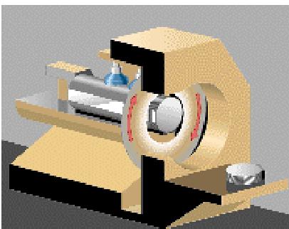
29 Effusion cells Basic schematic small aperture Real example Temperature control is very important since temperature controls equilibrium vapour pressure, and hence deposition rate solid close to equilibrium with gas Heat Shutter over aperture must operate very quickly to ensure fast switching between beams of different elements (e.g. In, Ga) and achieve sharp interfaces.