Ex: NaCl. Ironically Bonded Solid
|
|
|
- Moris Baker
- 5 years ago
- Views:
Transcription
1
2 Ex: NaCl. Ironically Bonded Solid
3
4
5


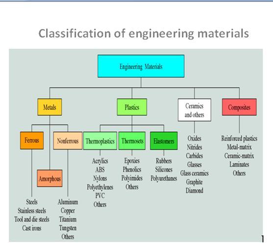
6 Lecture 2 THE STRUCTURE OF CRYSTALLINE SOLIDS 3.2 FUNDAMENTAL CONCEPTS SOLIDS AMORPHOUS CRYSTALLINE Atoms in an amorphous Atoms in a crystalline solid solid are arranged are arranged in a repetitive randomly- No Order three dimensional pattern Long Range Order All metals are crystalline solids Many ceramics are crystalline solids Some polymers are crystalline solids
7

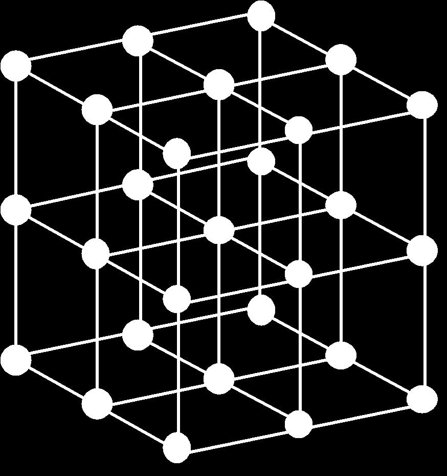
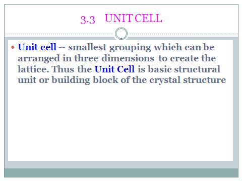
8 Unit cell & Lattice Lattice Unit Cell


 order to have lower bonding energy.")
9 3.4 METALLIC CRYSTALS Tend to be densely packed. Have several reasons for dense packing: -Typically, only one element is present, so all atomic radii are the same. -Metallic bonding is not directional. -Nearest neighbor distances SIMPLE tend CUBIC to be STRUCTURE small in (SC) order to have lower bonding energy. Let us look at three such structures... 4 SC structure
10 BODY CENTERED CUBIC STRUCTURE (BCC) Cr, Fe, W, Nb, Ba, V FACE CENTERED CUBIC STRUCTURE (FCC)

11 HEXAGONAL CLOSE-PACKED STRUCTURE HCP Mg, Zn, Cd, Zr, Ti, Be BCC FCC Number of atoms per unit cell 1/8 corner atom x 8 corners + 1 body center atom =2 atoms/uc 1/8 corner atom x 8 corners + ½ face atom x 6 faces =4 atoms/uc HCP 3 inside atoms + ½ basal atoms x 2 bases + 1/ 6 corner atoms x 12 corners =6 atoms/uc
12 Relationship between atomic radius and edge lengths For FCC: a = 2R 2 For BCC: a = 4R / 3 For HCP a = 2R c/a = (for ideal case) Note: c/a ratio could be less or more than the ideal value of Face Centered Cubic (FCC) 2a0 4r r 2r r a 0 a 0
13 Body Centered Cubic (BCC) 3a0 4r 2a 0 a 0 3a 0 Coordination Number The number of touching or nearest neighbor atoms SC is 6 BCC is 8 FCC is 12 HCP is 12


14 ATOMIC PACKING FACTOR APF for a simple cubic structure = ATOMIC PACKING FACTOR: BCC APF for a body-centered cubic structure = 0.68 a = 4R / 3 R a Unit cell contains: x 1/8 = 2 atoms/unit cell
15 FACE CENTERED CUBIC STRUCTURE (FCC) Close packed directions are face diagonals. --Note: All atoms are identical; the face-centered atoms are shaded differently only for ease of viewing. Coordination # = 12 ATOMIC PACKING FACTOR: FCC APF for a face-centered cubic structure = 0.74 a = 2R 2 a Unit cell contains: 6 x 1/2 + 8 x 1/8 = 4 atoms/unit cell

16 3.5 Density Computations Density of a material can be determined theoretically from the knowledge of its crystal structure (from its Unit cell information) Density mass/volume Mass is the mass of the unit cell and volume is the unit cell volume. mass = ( number of atoms/unit cell) n x mass/atom mass/atom = atomic weight A /Avogadro s Number N A Volume = Volume of the unit cell V c THEORETICAL DENSITY
17 Example problem on Density Computation Problem: Compute the density of Copper Given: Atomic radius of Cu = nm (1.28 x 10⁻⁸ cm) Atomic Weight of Cu = 63.5 g/mol Crystal structure of Cu is FCC Solution: = n A / V c N A n = 4 V c = a 3 = (2R 2) 3 = 16 R 3 2 N A = x atoms/mol = 4 x 63.5 g/mol / 16 2(1.28 x 10⁻⁸ cm) 3 x x atoms/mol Ans = 8.98 g/cm 3 Experimentally determined value of density of Cu = 8.94 g/cm Crystal Systems Since there are many different possible crystal structures, it is sometimes convenient to divide them into groups according to unit cell configurations and/or atomic arrangements. One such scheme is based on the unit cell geometry, i.e. the shape of the appropriate unit cell parallelepiped without regard to the atomic positions in the cell. Within this framework, an x, y, and z coordinate system is established with its origin at one of the unit cell corners; each x, y, and z-axes coincides with one of the three parallelepiped edges that extend from this corner, as illustrated in Figure.

18 The Lattice Parameters Lattice parameters a, b, c,,, are called the lattice Parameters. 3.7 Point Coordinates in an Orthogonal Coordinate System Simple Cubic
19 3.8 MILLER INDICES FOR CRYSTALLOGRAPHIC PLANES Miller Indices for crystallographic planes are the reciprocals of the fractional intercepts (with fractions cleared) which the plane makes with the crystallographic x,y,z axes of the three nonparallel edges of the cubic unit cell. 4-Step Procedure: 1. Find the intercepts that the plane makes with the three axes x,y,z. If the plane passes through origin change the origin or draw a parallel plane elsewhere (e.g. in adjacent unit cell) 2. Take the reciprocal of the intercepts 3. Remove fractions 4. Enclose in ( ) Crystallographic Planes z example a b c 1. Intercepts 1 1 c 3. Reduction Miller Indices (110) example a b c 1. Intercepts 1/2 a x z c b y Reduction Miller Indices (200) a x b y

20 Crystallographic Directions in Cubic System [210]
21 Atomic Arrangement on (110) plane in FCC
22
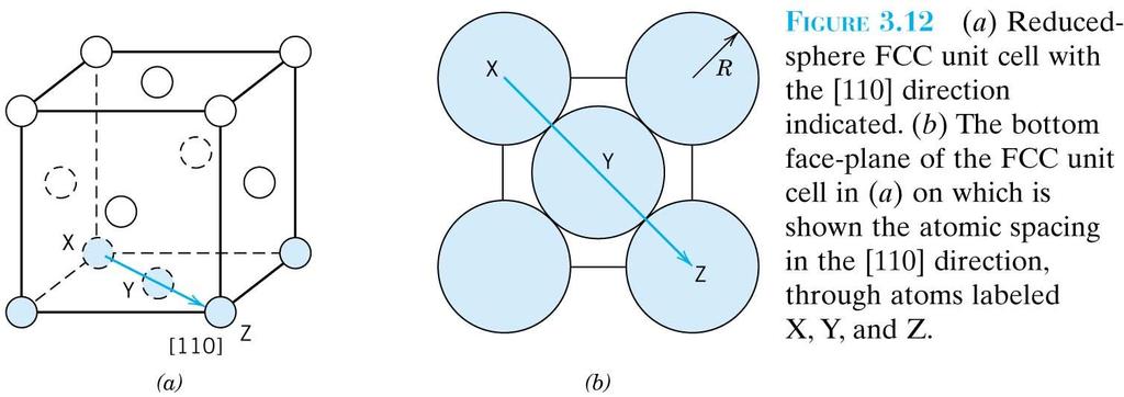
![Linear Density LD for [110] in BCC.](/docs-images/96/127334370/images/23-0.jpg "# of atom centered on the direction vector [110] = 1/2 +1/2 = 1 Length of direction vector [110] = 2 a")
![a = 4R/ 3 LD 1 2a 1 2(4R / 3) 3 24R [110] 2a LD of [110] in FCC # of atom centered on the direction](/docs-images/96/127334370/images/23-2.jpg "vector [110] = 2 atoms Length of direction vector [110] = 4R Linear Density LD = 2 /4R LD = 1/2R Linear")
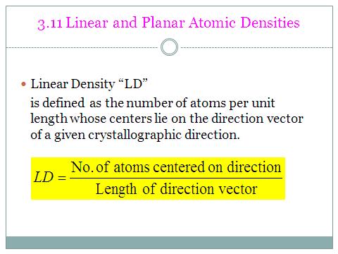
23 Linear Density LD for [110] in BCC. # of atom centered on the direction vector [110] = 1/2 +1/2 = 1 Length of direction vector [110] = 2 a a = 4R/ 3 LD 1 2a 1 2(4R / 3) 3 24R [110] 2a LD of [110] in FCC # of atom centered on the direction vector [110] = 2 atoms Length of direction vector [110] = 4R Linear Density LD = 2 /4R LD = 1/2R Linear density can be defined as reciprocal of the repeat distance r LD = 1/r
24 Planar Density Planar Density PD is defined as the number of atoms per unit area that are centered on a given crystallographic plane. No of atoms centered on the plane PD = Area of the plane Planar Density of (110) plane in FCC # of atoms centered on the plane (110) = 4(1/4) + 2(1/2) = 2 atoms Area of the plane = (4R)(2R 2) = 8R 2 2 (111) Plane in FCC PD atoms 8R 2 2 4R a = 2R 2 4R

25 Hexagonal Close-Packed Structure (HCP) ABAB... Stacking Sequence 3D Projection A sites 2D Projection Top layer c B sites Middle layer a A sites Bottom layer Coordination # = 12 APF = 0.74 c/a = atoms/unit cell ex: Cd, Mg, Ti, Zn
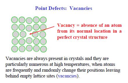
26 Crystalline and Noncrystalline Materials Single Crystals For a crystalline solid, when the periodic and repeated arrangement of atoms is perfect or extends throughout the entirety of the specimen without interruption, the result is a single crystal. All unit cells interlock in the same way and have the same orientation. Single crystals exist in nature, but may also be produced artificially. They are ordinarily difficult to grow, because the environment must be carefully controlled. Example: Electronic microcircuits, which employ single crystals of silicon and other semiconductors.
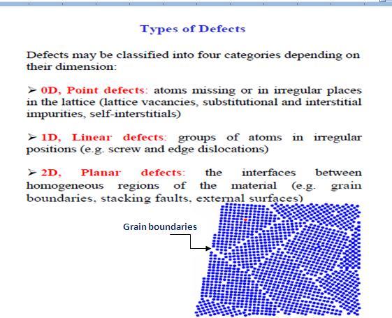
 Small crystallite nuclei Growth of the crystallites. b) Obstruction of some grains that are adjacent to one another is also shown.")
27 3.13 Polycrytalline Materials Polycrystalline crystalline solids composed of many small crystals or grains. Various stages in the solidification : a) Small crystallite nuclei Growth of the crystallites. b) Obstruction of some grains that are adjacent to one another is also shown. c) Upon completion of solidification, grains that are adjacent to one another is also shown. d) Grain structure as it would appear under the microscope. Polycrystalline Materials
28
29
30
31
32
 deformation by slip تمثيل حركة االنخالعة بحركة )دودة")
33 Shear occurs by dislocation movement producing permanent (plastic) deformation by slip تمثيل حركة االنخالعة بحركة )دودة القز(.
34
35