ALTIUMLIVE 2018: FLEX: SOMETHING NEW FOR EVERYONE
|
|
|
- Godfrey Marsh
- 5 years ago
- Views:
Transcription

1 ALTIUMLIVE 2018: FLEX: SOMETHING NEW FOR EVERYONE Tara Dunn Omni PCB President San Diego October 5, 2018


2
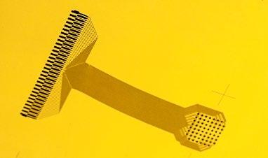


3 Applications That Span Technology
4 Today s Discussion: 1. Basic processing steps for both subtractive etch and semi-additive flexible circuit manufacturing 2. Flex materials and considerations 3. Design for manufacturability best practices 4. Real world lessons learned


5 Learning Curve for Everyone Conventional Board

6 Basic Process Steps PCB Fabrication Key differences between subtractive etch and SAP: Base materials Develop -Etch -Strip process Hole Metalization


7 Basic Inner Layer Process Steps Subractive Etch


8 Basic Inner Layer Process Steps Subractive Etch

9 Basic Inner Layer Process Steps Semi Additive Processing 1. Start with polyimide film 2. Coat polyimide with ALD Ink 3. Plate with thin electroless copper 4. Apply and pattern resist 5. Electroplate traces 6. Strip resist and remove thin electroless copper

10 Basic Process Steps Semi Additive Processing 35 µm pitch, 24 µm lines, semi additive 25 µm traces, polymide with gold conductors, semi additive

11 Base Material Types and Considerations Base Materials: Two Primary Construction Types


12 Base Material Types and Considerations How Do You Select Base Materials? 1. Layer Count 2. Flex or Rigid Flex 3. Cost 4. SAP


13 Coverlay Options and Considerations Liquid polyimide Cost vs. Function


14 Stiffener Options and Considerations Stiffener Types FR4 adds component support Maintain.030 overlap between stiffener and coverlay to avoid adding stress points Polyimide stiffeners


15 Rigid Flex Key Points: Adhesiveless Materials Bikini Cut the coverlay (.050 into the rigid areas) PTH should be.050 from edge of flex / rigid interface Cost Considerations


16 Design Tips Design for Manufacturability Tips: Universal across manufacturing types Key: Communicate operational requirements to your fabricator, especially with dynamically flexing applications


17 Design Tips Design for Manufacturability Tips Single Metal Layer: 3-6 times material thickness Two Metal Layers: 7-10 times material thickness Multilayer Flex: times material thickness Dynamic Flexing: times material thickness. Thru holes should be placed at least.050 away from any bend areas


18 Design Tips Tips and Tricks for increased flexibility Cross hatch copper Remove Material Route traces to second side and remove copper in flexing area Un-bonded layers Consider Button-Plating to eliminate ED copper on panel when creating the PTH


19 Real World Lesson Learned Case Study Medical Pill Camera: Rigid-Flex 4 Layer PCB Very small part.5 by 1 in size on 15-up array. The part is ingested in pill form. PROBLEM: Customer had soldering issues on Micro BGA High volume offshore solution needed 100K+ pieces annually SOLUTION: Offered via fill solution Implemented copper filled vias in 4 mil holes for Micro BGA pads After solution was implemented the customer had zero rejects Qualified off shore partner for high volume production Shipped over 100K parts


20 Real World Lesson Learned Case Study Avionics Application: Rigid-Flex 4 Layer PCB with 2 stiffeners PROBLEM: Customer had 70% failure rate from existing supplier Copper in Flex area was cracking due to flex area of PCB being bent several times SOLUTION: Redesigned stack-up Converted customer to adhesiveless kapton material Decreased Flex Circuit thickness from 19.6 mils to 13.4 mils a 32% decrease Extra thickness was adding rigidity to flex area and causing copper to crack once circuit was bent to form application Part is populated, bent to shape and shipped to customer. Now qualified on a 12 year program with customer

21 Real World Lesson Learned Materials and Metal System for Neural Probes Neural probes for brain stimulation Unique gold on polyimide without any tie layer - - ideal for In Situ applications 25 um leads 64 leads per side NYU / Duke / Univ. of PA research consortium A single metal system and reliable materials proved to be the best for this and other implanted probe applications The overall simplicity leads to fewer manufacturing steps and greater yield and reliability


22 Real World Lesson Learned Case Study: Integrating Subtractive Etch Layers with SAP Layers PROBLEM: High density routing requires every layer via design Ten layer design requires 4 lamination cycles, which is both expensive and has an extended lead time SOLUTION: Convert 4 of the 10 layers to SAP with 1 mil line and space Reduce the total number of layers needed to 8 Integrate the SAP layers with 4 layers of subtractive etch processing Reduce the lamination cycles required from 1 to 4 In development now with future development planned with LIP-C processing

23 Thank you!
Flexible Printed Circuits Design Guide
 www.tech-etch.com/flex Flexible Printed Circuits Design Guide Multilayer SMT Assembly Selective Plating of Gold & Tin-Lead Fine Line Microvias Cantilevered & Windowed Leads 1 MATERIALS CONDUCTOR Copper
Welcome to Streamline Circuits Lunch & Learn. Design for Reliability & Cost Reduction of Advanced Rigid-Flex/Flex PCB Technology
 Welcome to Streamline Circuits Lunch & Learn Design for Reliability & Cost Reduction of Advanced Rigid-Flex/Flex PCB Technology Accurate PCB data is critical to the tooling process. Here are some key items
Why Flex? Capabilities. Why PCi?
 Why Flex? Innovation Flexible circuits give you a unique tool to bring your innovative packaging ideas to market, and to separate your products from the crowd. Flex gives you the ability to create circuitry
Deepen your knowledge
 FLEX & RIGID-FLEX PRINTED CIRCUIT BOARDS Deepen your knowledge What are Flex & Rigid-flex Printed Circuit Boards? What are their similarities and differences? Their capabilities? And the design rules.
PCB Production Process HOW TO PRODUCE A PRINTED CIRCUIT BOARD
 NCAB Group Seminars PCB Production Process HOW TO PRODUCE A PRINTED CIRCUIT BOARD NCAB GROUP PCB Production Process Introduction to Multilayer PCBs 2 Introduction to multilayer PCB s What is a multilayer
Company Overview Markets Products- Capabilities
 Company Overview Markets Products- Capabilities A Simpler way for PCB production. www.purepcb.co.uk What can Pure do for you? From 1 off Circuit upward, No MOQ/MOV High Mix Production Focus. Fast Turn
Qualification and Performance Specification for Flexible Printed Boards
 Qualification and Performance Specification for Flexible Printed Boards Developed by the Flexible Circuits Performance Specifications Subcommittee (D-12) of the Flexible Circuits Committee (D-10) of IPC
Flex and Rigid flex boards. 02/2013 Written by Zreik Anan
 Flex and Rigid flex boards 02/2013 Written by Zreik Anan Advantages Better Reliability Dynamic flexing Replace cables (Static Flexing) Simplify assembly process Less rework Saves money Materials Flex clad
iniaturization of medical devices thanks to flexible substrates ISO 9001 certified
 iniaturization of medical devices thanks to flexible substrates 04-12-2012 Hightec MC Presentation 2 Medical industry is clearly and urgently in need of the development of advanced interconnection solutions
Innovative PCB Solutions. Win time and flexibility benefit from Swiss quality. THE PCB CHALLENGE Doing it together
 Innovative PCB Solutions Win time and flexibility benefit from Swiss quality THE PCB CHALLENGE Doing it together INDIVIDUAL CUSTOMER SOLUTIONS from a reliable partner 2 Optiprint offers consulting, development
FLEXIBLE & RIGID-FLEX CIRCUITS TECHNICAL ENGINEERING GUIDE. Delivering Quality Since 1952.
 FLEXIBLE & RIGID-FLEX CIRCUITS TECHNICAL ENGINEERING GUIDE Delivering Quality Since 1952. DELIVERING QUALITY SINCE 1952. Epec Engineered Technologies designs and manufactures customized, built-to-print,
PCB Fabrication Specification
 Original Author: Steve Babiuch Process Owner: Steve Babiuch Page 2 of 8 1.0 Purpose This specification establishes the NEO Tech fabrication requirements for printed circuit boards. The order of precedence
FABRICATING HIGH CURRENT, HEAVY COPPER PCBS
 Royal Circuit Solutions 21 Hamilton Ct, Hollister, CA 95023 (831) 636-7728 www.royalcircuits.com FABRICATING HIGH CURRENT, HEAVY COPPER PCBS INTRODUCTION All printed circuit boards (PCBs) carry current
!"#$#%&#'(() ) **+,-./01)2-,-.3)456,1) /0! **)
 ) **+,-./01)2-,-.3)456,1) /0! **)") !"#$#%&#'(() ) **+,-./01)2-,-.3)456,1) /0!7.5853-09**) B 2 IT is a Toshiba Process Technology 1. Conductive Ag bumps are printed on a sheet of Cu foil. 2. Prepreg is pierced through by the bumps 3. Another
!"#$#%&#'(() ) **+,-./01)2-,-.3)456,1) /0!7.5853-09**) B 2 IT is a Toshiba Process Technology 1. Conductive Ag bumps are printed on a sheet of Cu foil. 2. Prepreg is pierced through by the bumps 3. Another
Flex and Rigid-Flex Printed Circuit Design
 Flex and Rigid-Flex Printed Circuit Design Old Content - visit altium.com/documentation Modified by on 29-Nov-2016 Related Videos Bending Lines Enhanced Layer Stack Management Layer Stack Regions A rigid-flex
Manufacturing Capacity
 Capability List Manufacturing Capacity QTA & Prototype Layer : 1L ~32 L Impedance Board Ball Grid Array ( BGA ) Blind/ Buried Via Micro Via ( Laser Drilling) Flex /Rigid Flexible PCB Series Orders Layer
(13) PCB fabrication / (2) Focused assembly
 PCB fabrication / (2) Focused assembly") Company Fact Sheet TTM Technologies, Inc. is a world-wide leader in the manufacture of technologically advanced PCBs, backplane and sub-system assemblies. Our Global Presence / Local Knowledge approach
Company Fact Sheet TTM Technologies, Inc. is a world-wide leader in the manufacture of technologically advanced PCBs, backplane and sub-system assemblies. Our Global Presence / Local Knowledge approach
Precision Engineered Parts
 Precision Engineered Parts Photoetching Laser Cutting Forming Finishing Thin Metal Parts Flexible Circuits EMI Shielding Gaskets www.tech-etch.com PHOTOETCHING Tech-Etch specializes in the manufacture
GRAPHIC MANUFACTURING CAPABILITY Q217-18
 All features are design dependent and may not be achievable in combination Reduced Yield / Special values up ( or down ) to the standard limit are design and application dependent Standard features only
Freescale Semiconductor Tape Ball Grid Array (TBGA) Overview
 Overview") Freescale Semiconductor Tape Ball Grid Array (TBGA) Overview Revision 0 2006 Freescale and the Freescale logo are trademarks of Freescale Semiconductor, Inc. All other product or service names are the
Freescale Semiconductor Tape Ball Grid Array (TBGA) Overview Revision 0 2006 Freescale and the Freescale logo are trademarks of Freescale Semiconductor, Inc. All other product or service names are the
CANDOR Industries Inc. High Quality PCB Manufacturing Solutions
 CANDOR Industries Inc High Quality PCB Manufacturing Solutions 1 Our Mission Founded in 1999, Candor is an industry leader in High Technology Printed Circuit Board Fabrication Services. Quick turn services
The Anatomy of a PCB SINGLE-SIDED BOARD
 Published on Online Documentation for Altium Products (https://www.altium.com/documentation) 主页 > The Board Using Altium Documentation Modified by Jason Howie on Apr 11, 2017 Open up just about any electronic
Building HDI Structures using Thin Films and Low Temperature Sintering Paste
 Building HDI Structures using Thin Films and Low Temperature Sintering Paste Catherine Shearer, James Haley and Chris Hunrath Ormet Circuits Inc. - Integral Technology California, USA chunrath@integral-hdi.com
Smart PCBs. Work
 0 Smart PCBs Service Road, Shaheen Town, near Airport Chowk, Rawalpindi, 4600, PAKISTAN Tel: +92 (0) 51 457 8047, Fax (0) 51 457 8048 www.smartpcbs.com Dear Sir/Madam, SmartPCBs is the leading fabricators
Technology HF-Printed Circuits Rev For latest information please visit
 Options and Characteristics Online calculation On explicit enquiry Quantity 1 piece up to 0,4m² total area from 1 piece to mass production Layer quantity 1 to 2 layers Up to 8 layers Material thickness
The Essential Role of DFx In The Lean Smart New Product Introduction (NPI) Flow
 Flow") The Essential Role of DFx In The Lean Smart New Product Introduction (NPI) Flow Presenter: Michael Ford Title: Marketing Development Manager Date: 16 th March 2017 Today s Agenda What is Industry 4.0 and
The Essential Role of DFx In The Lean Smart New Product Introduction (NPI) Flow Presenter: Michael Ford Title: Marketing Development Manager Date: 16 th March 2017 Today s Agenda What is Industry 4.0 and
Bending Impacts Layers
 Designing for Flexibility and Reliability Understanding factors that contribute to the reliability of a flex circuit that is formed or repeatedly flexed The name "flexible circuit" sums up the function
How Printed Circuit Boards are Made. Todd Henninger Field Applications Engineer Midwest Region
 PCB 101: How Printed Circuit Boards are Made Todd Henninger Field Applications Engineer Midwest Region Tooling PRE-PRODUCTION ENGINEERING (Tooling) Design Data Package CAD Data (ODB++ or Gerber 274x format)
Basic 4-layer manufacturing process
 Basic 4-layer manufacturing process Erwin Lemmens - AQC BV 7-11 D&E BE / Booth 1 8-11 D&E NL / Booth 18 AQC (Advanced Quality Control) BV Supplying pcb s, flex, flex-rigids, aluminium, etc - standard and
Equipment & Processes
 Equipment & Processes The Circuits facility was designed for defect-free manufacturing of ex and rigid-ex printed circuit boards exclusively. The equipment and processes were chosen to minimize the handling
Technology Aluminium-IMS-PCBs Rev For latest information please visit
 Options and Characteristics Online calculation On explicit enquiry Quantity 1 piece up to 1,0² total area from 1 piece to mass production Layer quantity 1- and 2-layers up to 6 layers Material thickness
New Developments in PCB Laminates. Dean Hattula, John Coonrod Rogers Corporation Advanced Circuit Materials Division
 New Developments in PCB Laminates Dean Hattula, John Coonrod Rogers Corporation Advanced Circuit Materials Division Overview PCB laminate properties Thermal stability Electrical performance Summary PCB
IMPACT OF MICROVIA-IN-PAD DESIGN ON VOID FORMATION
 IMPACT OF MICROVIA-IN-PAD DESIGN ON VOID FORMATION Frank Grano, Felix Bruno Huntsville, AL Dana Korf, Eamon O Keeffe San Jose, CA Cheryl Kelley Salem, NH Joint Paper by Sanmina-SCI Corporation EMS, GTS
Flexible PCB Plating Through Hole Considerations, Experiences and Solutions
 Presented in the ECWC 10 Conference at IPC Printed Circuits Expo, SMEMA Council APEX and Designers Summit 05 Flexible PCB Plating Through Hole Considerations, Experiences and Solutions Neil Patton Atotech
Embedding of Active Components in LCP for Implantable Medical Devices
 44 th IMAPS New England Symposium 2017 Embedding of Active Components in LCP for Implantable Medical Devices Dr. Eckardt Bihler and Dr. Marc Hauer, Dyconex AG Susan Bagen, PE, Micro Systems Technologies,
ALTIUMLIVE 2018: NAVIGATING THE COMPLEXITIES OF PCB MATERIAL SELECTION
 ALTIUMLIVE 2018: NAVIGATING THE COMPLEXITIES OF PCB MATERIAL SELECTION Chris Hunrath Insulectro, VP of Technology San Diego October 4 Outline 1 PCB Material Overview 2 What is the Dielectric Constant of
Axiom Electronics LLC
 1 of 8 1.0 PURPOSE and SCOPE This document defines Axiom s requirements for printed circuit board (PCB) fabrication, handling, and storage. Industry standards are referenced where appropriate. This document
3M Electrically Conductive Adhesive Transfer Tape 9707
 Technical Data May 2014 3M Electrically Conductive Adhesive Transfer Tape 9707 Product Description 3M Electrically Conductive Adhesive Transfer Tape (ECATT) 9707 is a pressure sensitive adhesive (PSA)
PRODUCTION SERVICE OF PRINTED CIRCUIT BOARDS (PCBS)
") PRODUCTION SERVICE OF PRINTED CIRCUIT BOARDS (PCBS) TESAT PCB - Manufacturing PROPRIETARY INFORMATION Tesat-Spacecom GmbH & Co. KG reserves all rights including industrial property rights, and all rights
PRODUCTION SERVICE OF PRINTED CIRCUIT BOARDS (PCBS) TESAT PCB - Manufacturing PROPRIETARY INFORMATION Tesat-Spacecom GmbH & Co. KG reserves all rights including industrial property rights, and all rights
14. Designing with FineLine BGA Packages
 14. Designing with FineLine BGA Packages S51014-1.0 Chapter 14, Designing with FineLine BGA Packages, replaces AN 114: Designing with FineLine BGA Packages. Introduction As programmable logic devices (PLDs)
All-Polyimide Thermal Interface Products
 All-Polyimide Thermal Interface Products SMTA Harsh Environment Electronics Workshop Dearborn, MI 6/24/03 Jim Fraivillig Fraivillig Technologies Boston, MA Why polyimide? HARSH ENVIRONMENT ELECTRONICS.
PRINTED CIRCUITS HANDBOOK
 PRINTED CIRCUITS HANDBOOK Clyde F. Coombs, Jr. Sixth Edition Me Graw New York Chicago San Francisco Lisbon London Madrid Mexico City Milan New Delhi San Juan Seoul Singapore Sydney Toronto CONTENTS List
Option Technologies. Ventec International Group Offshore Masslam Solutions From Prototype To Volume. Drilled Masslam from Taiwan
 Option Technologies Ventec International Group Offshore Masslam Solutions From Prototype To Volume Drilled Masslam from Taiwan Manufacturing Capabilities Capabilities Maximum Layer Count 34 Maximum Panel
Fairchild Semiconductor Application Note January 2001 Revised September Using BGA Packages
 Introduction AN-5026 Demanding space and weight requirements of personal computing and portable electronic equipment has led to many innovations in IC packaging. Combining the right interface and logic
Current Standards Flex-Rigid
 Current Standards Flex-Rigid Würth Elektronik Circuit Board Technology Webinar April 17th, 2018 Speaker: Andreas Schilpp www.we-online.com page 1 19.04.2018 agenda 1 2 3 4 WHY Flex-Rigid? Hierarchy of
Designing With High-Density BGA Packages for Altera Devices. Introduction. Overview of BGA Packages
 Designing With High-Density BGA Packages for Altera Devices December 2007, ver. 5.1 Application Note 114 Introduction As programmable logic devices (PLDs) increase in density and I/O pins, the demand for
PEC (Printed Electronic Circuit) process for LED interconnection
 process for LED interconnection") PEC (Printed Electronic Circuit) process for LED interconnection Higher wattage LED s/ power components or their placement in higher densities, requires a larger dissipation of heat in a more effective
PEC (Printed Electronic Circuit) process for LED interconnection Higher wattage LED s/ power components or their placement in higher densities, requires a larger dissipation of heat in a more effective
Chapter 14. Designing with FineLine BGA Packages
 Chapter 14. Designing with FineLine BGA Packages S53009-1.3 Chapter 14, Designing with FineLine BGA Packages, replaces AN 114: Designing with FineLine BGA Packages. Introduction As programmable logic devices
Fine Pitch P4 Probe Cards
 Fine Pitch P4 Probe Cards Photolithographic Pattern Plating Process June 1998 By Toshi Ishii, Hide Yoshida Contents What is a P4 probe card? Specification Some test results Tip cleaning RF performance
SURFACE-MOUNTING OF POWER DEVICES TO ALUMINUM HEAT SINKS
 TO ALUMINUM HEAT SINKS SMTA PanPacific Thermal Management Hawaii March 11, 2004 Jim Fraivillig Fraivillig Technologies Boston, MA PowerSite technology. Convert aluminum heat sinks to surface-mount applications
Flex-Rigid Design Guide
 DESIGN GUIDE Version 1.2 / March 2018 Flex-Rigid Design Guide The trend to miniaturization in electronics continues. Integrated circuit board solutions are becoming more and more popular as a means of
ATS Document Cover Page
 221-008 Item Rev Status: RELEASED printed 9/20/2017 2:27:42 PM by Les Deenin ATS: OPERATIN PROCEDURE ATS Document Cover Page Responsible Department: Supply Chain This copy is uncontrolled unless otherwise
UL PCB Recognition what is it & why do you need to know about it
 UL PCB Recognition what is it & why do you need to know about it Presented by Emma Hudson NCAB Customer Event March 2015 UL and the UL logo are trademarks of UL LLC 2015 Agenda What is UL and what are
Stevenage Circuits Group
 Stevenage Circuits Group Incorporating: Stevenage Circuits Tru-Lon Printed Circuits March 2011 The Organisation Stevenage Circuits formed 1971 Tru-Lon integrated into the Stevenage site March 2011 Group
Advances in Printing nano Cu and Using Existing Cu Based Manufacturing Processes. Michael J. Carmody Chief Scientist, Intrinsiq Materials
 Advances in Printing nano Cu and Using Existing Cu Based Manufacturing Processes Michael J. Carmody Chief Scientist, Intrinsiq Materials Why Use Copper? Lower Cost than Silver. Print on Numerous Substrates.
Sales Presentation. GoldenTechCircuits Technology Co.LTD 鑫科电路技术有限公司. Professional QTA & HMLV PCB Manufacturer
 GoldenTechCircuits Technology Co.LTD 鑫科电路技术有限公司 Professional QTA & HMLV PCB Manufacturer General Information Established Date: Nov, 2009 Capital: USD 1.5 Million Brazil Office:Travessa Rolante, 40 - Corcunda
Advances in Printing nano Cu and Using Existing Cu Based Manufacturing Processes. Michael J. Carmody Chief Scientist, Intrinsiq Materials
 Advances in Printing nano Cu and Using Existing Cu Based Manufacturing Processes Michael J. Carmody Chief Scientist, Intrinsiq Materials Why Use Copper? Lower Cost than Silver. Print on Numerous Substrates.
3M XYZ / Isotropic Electrically Conductive Adhesive Transfer Tape 9709
 Technical Data October, 2009 3M XYZ / Isotropic Electrically Conductive Adhesive Transfer Tape 9709 Product Description 3M XYZ/Isotropic Electrically Conductive Adhesive Transfer Tape 9709 is a pressure
MACDERMID ENTHONE ELECTRONICS SOLUTIONS BLACKHOLE/ECLIPSE
 MACDERMID ENTHONE ELECTRONICS SOLUTIONS BLACKHOLE/ECLIPSE DEC, 2016 OUTLINE Mechanism of Blackhole / Eclipse Blackhole / Eclipse process - Sequence - Process Equipment enhancement Performance test method
- 1 - Contents. Date: Date changed Made by: PCB Technical. Accepted by: Gordon Falconer
 - - page of 4 Contents Inner and outer layer features... 2. Description... 2.2 Capability... 2 2 Build-up / Multilayer... 3 2. Common capability... 3 Standard build-up... 3 3 Drilling/Routing/V-cut/Bevel...
ROLINX Laminated Busbar. Design Rules Version 01 (12/2015)
") ROLINX Laminated Busbar Design Rules Version 01 (12/2015) Content 1. Introduction... 03 7. Features... 13 2. Configuration...03 8. Thermal parameters... 14 3. Products... 04 9. General parameters... 14
ROLINX Laminated Busbar Design Rules Version 01 (12/2015) Content 1. Introduction... 03 7. Features... 13 2. Configuration...03 8. Thermal parameters... 14 3. Products... 04 9. General parameters... 14
Embedded Passives..con0nued
 Embedded Passives..con0nued Why Embedded Passives? Improves the packaging efficiency System-on-Package (SOP); SLIM integration Reducing size Eliminating substrate assembly Minimizing solder joint failure
Introduction Conductors. Supply Planes. Dielectric. Vias PCB Manufacturing Process Electronic Assembly Manufacturing Process
 PCBs/Overview Printed Circuit Boards (PCB) Introduction Conductors. Supply Planes. Dielectric. Vias PCB Manufacturing Process Electronic Assembly Manufacturing Process 29/09/2005 EE6471 (KR) 263 PCBs/Overview
Ready For The Future 2016
 Ready For The Future 2016 Your Full Service, Time Sensitive, Printed Circuit Board Solution Located in the Heart of Silicon Valley, Streamline Circuits is your premier PCB manufacture of leading edge Technology
Offshore Wind Turbines Power Electronics Design and Reliability Research
 Offshore Wind Turbines Power Electronics Design and Reliability Research F. P. McCluskey CALCE/Dept. Of Mechanical Engineering University of Maryland, College Park, MD (301) 405-0279 mcclupa@umd.edu 1
The Development of a Novel Stacked Package: Package in Package
 The Development of a Novel Stacked Package: Package in Package Abstract Stacked die Chip Scale Packages (CSPs) or Fine-pitch BGAs (FBGAs) have been readily adopted and integrated in many handheld products,
Chips Face-up Panelization Approach For Fan-out Packaging
 Chips Face-up Panelization Approach For Fan-out Packaging Oct. 15, 2015 B. Rogers, D. Sanchez, C. Bishop, C. Sandstrom, C. Scanlan, TOlson T. REV A Background on FOWLP Fan-Out Wafer Level Packaging o Chips
100 WAYS TO REDUCE COST
 OPTIMUM DESIGN S 100 WAYS TO REDUCE COST COST SAVING TIPS FOR PCB ASSEMBLY 1 100 Ways to Reduce Cost SUMMARY 57 Ideas For Engineers 16 Things Buyers Can Do Now 32 Ways MFG Can Cut Cost CONTENTS Design...
Design and Manufacturing of a Flexible Hybrid Electronics (FHE) Biometric Human Performance Monitor (BHPM)
 Biometric Human Performance Monitor (BHPM)") Design and Manufacturing of a Flexible Hybrid Electronics (FHE) Biometric Human Performance Monitor (BHPM) Presented by Professor Mark Poliks Systems Science and Industrial Engineering Binghamton University
Design and Manufacturing of a Flexible Hybrid Electronics (FHE) Biometric Human Performance Monitor (BHPM) Presented by Professor Mark Poliks Systems Science and Industrial Engineering Binghamton University
Optimizing Immersion Silver Chemistries For Copper
 Optimizing Immersion Silver Chemistries For Copper Ms Dagmara Charyk, Mr. Tom Tyson, Mr. Eric Stafstrom, Dr. Ron Morrissey, Technic Inc Cranston RI Abstract: Immersion silver chemistry has been promoted
High Definition Selective Metallization for Printed Electronics
 High Definition Selective Metallization for Printed Electronics Wolfgang Decker VAST FILMS, Ltd. Outline Introduction of VAST FILMS What is Selective Metalization Range of Applications for Selective Metalization
Flexible Substrates for Smart Sensor Applications
 Flexible Substrates for Smart Sensor Applications A novel approach that delivers miniaturized, hermetic, biostable and highly reliable smart sensor modules. AUTHORS Dr. Eckardt Bihler, Dr. Marc Hauer,
Implementation of IECQ Capability Approval using the IPC-6010 series of Standards
 Page 1 of 13 INTERNATIONAL ELECTROTECHNICAL COMMISSION QUALITY ASSESSMENT SYSTEM FOR ELECTRONIC COMPONENTS (IECQ) DOCUMENT NUMBER: OD 301 DOCUMENT TYPE: Operational Document VERSION: Version 1 TITLE: Implementation
Optimizing Immersion Silver Chemistries For Copper
 Optimizing Immersion Silver Chemistries For Copper Ms Dagmara Charyk, Mr. Tom Tyson, Mr. Eric Stafstrom, Dr. Ron Morrissey, Technic Inc Cranston RI Abstract: Immersion silver chemistry has been promoted
10 Manor Parkway, Suite C Salem, New Hampshire
 Micro-Precision Technologies (MPT) is an independent manufacturer of hybrid integrated circuits, multichip modules, and high-precision thick film substrates for the military, medical, avionics, optoelectronics,
RO4835T Core/RO4450T Bonding Layers Multi-Layer Board Processing Guidelines
 Fabrication Technical Articles Notes RO4835T Core/RO4450T Bonding Layers Multi-Layer Board Processing Guidelines These guidelines were developed to provide fabricators basic information on processing core
 Thermo-Mechanical Analysis of Flexible and Stretchable Systems Mario Gonzalez 1, Bart Vandevelde 1, Wim Christiaens 2, Yung-Yu Hsu 1, François Iker 1, Frederick Bossuyt 1, Jan Vanfleteren 1,2, Olaf van
Additive Circuit Technology Roadmap for HDD Suspension
 Additive Circuit Technology Roadmap for HDD Suspension Speaker: Hitoki KANAGAWA Prepared by Y.Ooyabu Approved by T.Visit (PhD) NOTE; The contents of this data sheet are the exclusive property of NITTO
Liquid Crystal Polymer Substrates to Enable Advanced RF and Medical Applications
 Liquid Crystal Polymer Substrates to Enable Advanced RF and Medical Applications Susan Bagen & Brian Sinclair MST Inc. Eckardt Bihler, Marc Hauer & Daniel Schulze DYCONEX AG New England 42nd Symposium
Corporate Presentation
 Corporate Presentation Sales History NA PCB Industry s Peak NA PCB Industry s Trough Company Profile Established 1985 100% Equity Owners / Full-Time Operators 115,000 ft² Facility (15,000 ft² warehouse)
Development of a Fluxless Flip Chip Bonding Process for Optical Military Electronics
 Development of a Fluxless Flip Chip Bonding Process for Optical Military Electronics Michael Girardi, Daric Laughlin, Philip Abel, Steve Goldammer, John Smoot NNSA s Kansas City Plant managed by Honeywell
Conductive Paste-Based Interconnection Technology for High Performance Probe Card
 Conductive Paste-Based Interconnection Technology for High Performance Probe Card Sang-il Kwon Eddy Kang TSE Co., Ltd. Overview Introduction of TABP Technology Key Technology of Core to Core Interconnection
Magnetization Fixture Design and Evaluation
 Magnetization Fixture Design and Evaluation 1 Overview Introduction Salient features of the magnetizing fixture design Following aspects have been discussed A. Effect of additional back iron during in-situ
Description. Spectro Tabs, higher purity conductive carbon tabs,12mm O.D.
 Description SPEC The simplicity of application and smooth, clean surfaces of PELCO Tabs Carbon Conductive Tabs are a significant improvement compared to many of the other common adhesives that have been
Chapter 4 Fabrication Process of Silicon Carrier and. Gold-Gold Thermocompression Bonding
 Chapter 4 Fabrication Process of Silicon Carrier and Gold-Gold Thermocompression Bonding 4.1 Introduction As mentioned in chapter 2, the MEMs carrier is designed to integrate the micro-machined inductor
Ultra Fine Pitch Bumping Using e-ni/au and Sn Lift-Off Processes
 Ultra Fine Pitch Bumping Using e-ni/au and Sn Lift-Off Processes Andrew Strandjord, Thorsten Teutsch, and Jing Li Pac Tech USA Packaging Technologies, Inc. Santa Clara, CA USA 95050 Thomas Oppert, and
Stackup Planning, Part 1
 by Barry Olney coulmn BEYOND DESIGN Stackup Planning, Part 1 The PCB substrate that physically supports the components, links them together via highspeed interconnects and also distributes highcurrent
Thermo-Mechanical Reliability of Through-Silicon Vias (TSVs)
") 1 Thermo-Mechanical Reliability of Through-Silicon Vias (TSVs) Xi Liu Ph.D. Student and Suresh K. Sitaraman, Ph.D. Professor The George W. Woodruff School of Mechanical Engineering Georgia Institute of
1 Thermo-Mechanical Reliability of Through-Silicon Vias (TSVs) Xi Liu Ph.D. Student and Suresh K. Sitaraman, Ph.D. Professor The George W. Woodruff School of Mechanical Engineering Georgia Institute of
STUDY OF IMMERSION GOLD PROCESSES THAT MAY BE USED FOR BOTH ENIG AND ENEPIG
 As originally published in the SMTA Proceedings STUDY OF IMMERSION GOLD PROCESSES THAT MAY BE USED FOR BOTH ENIG AND ENEPIG Don Gudeczauskas, Albin Gruenwald and George Milad UIC Technical Center Southington,
NiP Resistor Manufacturing Overview
 0 NiP Resistor Manufacturing Overview Thin film NiP resistive alloy material is made by electrodepositing of the NiP alloy onto copper foil (RESISTOR-CONDUCTOR MATERIAL) which is then laminated to a dielectric
Verifying The Reliability Of Connections In HDI PWBs
 Verifying The Reliability Of Connections In HDI PWBs The stacking of via holes is used effectively in the development of high density circuits on build-up printed wiring boards (PWBs). However, when micro
S/C Packaging Assembly Challenges Using Organic Substrate Technology
 S/C Packaging Assembly Challenges Using Organic Substrate Technology Presented by Bernd Appelt ASE Group Nov. 17, 2009 Overview The Packaging Challenge Chip Substrate Interactions Stiffeners for FC-BGA
Reliability Modeling of Electronics for Co-Designed System Applications Greg Caswell, DfR Solutions, LLC (o)
") DesignCon 2013 Reliability Modeling of Electronics for Co-Designed System Applications Greg Caswell, DfR Solutions, LLC gcaswell@dfrsolutions.com 301-640-5825 (o) 1 Abstract Complex electronic systems
DesignCon 2013 Reliability Modeling of Electronics for Co-Designed System Applications Greg Caswell, DfR Solutions, LLC gcaswell@dfrsolutions.com 301-640-5825 (o) 1 Abstract Complex electronic systems
Materials for High-Reliability Applications: All IPC-4101-Grouped Materials are not Created Equal
 they have arrived! f e a t u r e n e w a d v a n c e d p c b m a t e r i a l s Materials for High-Reliability Applications: All IPC-4101-Grouped Materials are not Created Equal By Yash Sutariya Saturn