ME 432 Fundamentals of Modern Photovoltaics. Discussion 30: Contacts 7 November 2018
|
|
|
- Samantha Chambers
- 5 years ago
- Views:
Transcription
1 ME 432 Fundamentals of Modern Photovoltaics Discussion 30: Contacts 7 November 2018


2 Fundamental concepts underlying PV conversion input solar spectrum light absorption carrier excitation & thermalization charge transport charge separation charge collection output You Are Here Courtesy: Yosuke Kanai, University of North Carolina
3 Learning Objectives: Contacts Describe the purpose of contacts, and the two main types of contacts used in the solar industry Describe what is meant by an ohmic and a Schottky contact, and the work function. Explain why we use large work function metals to make ohmic contacts to p-type semiconductors, and small work function metals to make ohmic contacts to n-type semiconductors Describe how contacts are typically incorporated into solar cells, and some common firing problems that can arise Describe how transparent conducting oxides work. That is, how are the both transparent and conducting at the same time?
4 Learning Objectives: Contacts Describe the purpose of contacts, and the two main types of contacts used in the solar industry Describe what is meant by an ohmic and a Schottky contact, and the work function. Explain why we use large work function metals to make ohmic contacts to p-type semiconductors, and small work function metals to make ohmic contacts to n-type semiconductors Describe how contacts are typically incorporated into solar cells, and some common firing problems that can arise Describe how transparent conducting oxides work. That is, how are the both transparent and conducting at the same time?

5 Contacts Purpose: extract electron and hole carrier from the interior of the solar cell, and deploy them into the external circuit Need to do this without allowing back-diffusion of carriers into the device Properties of a good contact: good conductor, inexpensive material, easy to manufacture, sturdy The best material to choose for a contact is very semiconductor specific. That is, silicon solar cells will use different contact materials than, e.g., CdTe cells. Two broad classifications of contacts: metals and transparent conducting oxides Transparent Conducting Oxides: optically transparent - Can be more expensive, but doesn t block the sun Metal Contacts: optically opaque - Can be fairly readily grown on top of thin-film cells - Usually less expensive, but does block sunlight
6 Learning Objectives: Contacts Describe the purpose of contacts, and the two main types of contacts used in the solar industry Describe what is meant by an ohmic and a Schottky contact, and the work function. Explain why we use large work function metals to make ohmic contacts to p-type semiconductors, and small work function metals to make ohmic contacts to n-type semiconductors Describe how contacts are typically incorporated into solar cells, and some common firing problems that can arise Describe how transparent conducting oxides work. That is, how are the both transparent and conducting at the same time?
7 What happens when we put a metal on a semiconductor? In general, two types of behavior can be observed. The contact can either be ohmic or rectifying (Schottky barrier) Ohmic contacts which freely allow current to flow in any direction, are most desirable Schottky barriers, which act a lot like pn junctions, are to be avoided.
8 What happens when we put a metal on a semiconductor? The type of contact depends on the relative work functions between the semiconductor and the metal The work function is, more or less, the energy required to completely remove an electron from a solid. It is equal to the difference between the Fermi energy and the vacuum level. E vac E work function f m E F work function f s E F metal semiconductors

9 Work Functions for Various Solids
10 Learning Objectives: Contacts Describe the purpose of contacts, and the two main types of contacts used in the solar industry Describe what is meant by an ohmic and a Schottky contact, and the work function. Explain why we use large work function metals to make ohmic contacts to p-type semiconductors, and small work function metals to make ohmic contacts to n-type semiconductors Describe how contacts are typically incorporated into solar cells, and some common firing problems that can arise Describe how transparent conducting oxides work. That is, how are the both transparent and conducting at the same time?
11 Ohmic or Rectifying? Whether the metal-semiconductor junction is ohmic of rectifying depends on the relative work functions of the semiconductor and metal: p-type semiconductor n-type semiconductor Ohmic f m > f s Rectifying f m < f s Rectifying Ohmic Thus, to achieve ohmic contacts on the n-type side of a solar cell, we need to use low work-function metals since we want f m < f s By contrast, to achieve ohmic contacts on the p-type side of a solar cell, we need to use high work-function metals.
12 Example of Ohmic Contact p-type semiconductor with f m > f s E vac E work function f m metal E F work function f s E F semiconductor
13 Example of Ohmic Contact p-type semiconductor with f m > f s E vac E work function f m work function f s E F metal E F semiconductor When the two are joined together, which way will the electrons flow? Recall that the Fermi energy represents the average energy of an electron electrons will flow from the semiconductor to the metal (high to low Fermi level) until the Fermi level equilibrates. Thus, electrons will diffuse from the semiconductor to the metal, resulting in a build up of electrons at the metal surface, and a depletion of electrons at the semiconductor surface
14 Example of Ohmic Contact p-type semiconductor with f m > f s E vac E metal E C Fermi level has dropped into the VB near the junction, and here the semiconductor acts like a metal E F E V semiconductor The flow will continue until the electric field that builds up across the junction creates a drift current that exactly cancels the diffusion current The final band diagram is shown above. The bands in the semiconductor bend upwards to reflect that the interface region is even more depleted of electrons. Because the Fermi level is inside the VB near the junction, the semiconductor behaves like a metal near the junction. Current can flow in any direction.

15 Example of Ohmic Contact p-type semiconductor with f m > f s An ohmic contact has a linear IV relationship, and there is no barrier to current flow in either direction
16 Example of Rectifying Contact n-type semiconductor with f m > f s E vac E work function f m metal E F work function f s E F semiconductor

17 Example of Rectifying Contact n-type semiconductor with f m > f s E vac E work function f m metal E F work function f s E F semiconductor When the two are joined together, which way will the electrons flow? Recall that the Fermi energy represents the average energy of an electron electrons will flow from the semiconductor to the metal (high to low Fermi level) until the Fermi level equilibrates. Thus, electrons will diffuse from the semiconductor to the metal, resulting in a build up of electrons at the metal surface, and a depletion of electrons at the semiconductor surface

18 Example of Rectifying Contact n-type semiconductor with f m > f s E vac E E C + E F Fermi level has dropped deep into the gap near the junction, and here the semiconductor conducts poorly metal semiconductor E V The flow will continue until the electric field that builds up across the junction creates a drift current that exactly cancels the diffusion current The final band diagram is shown above. The bands in the semiconductor bend upwards to reflect that the interface region is even more depleted of electrons. Because the Fermi level is deep inside the gap near the junction, the junction region is poorly conducting


19 Example of Rectifying Contact n-type semiconductor with f m > f s, no applied voltage E E vac Barrier for electrons moving from metal to semiconductor E C E F metal semiconductor E V With no applied voltage, note that there is a barrier for electrons moving in either direction

20 Example of Rectifying Contact n-type semiconductor with f m > f s, no applied voltage E E vac Barrier for electrons moving from semiconductor to metal E C E F metal semiconductor E V With no applied voltage, note that there is a barrier for electrons moving in either direction
21 Example of Rectifying Contact n-type semiconductor with f m > f s, positively biased E vac E E C E F metal semiconductor E V The applied bias, as drawn above, is called a forward or positive bias. Because it opposes (and hence reduces) the electric field at the junction, the degree of band bending in the semiconductor is also reduced

22 Example of Rectifying Contact n-type semiconductor with f m > f s, positively biased Direction of electron flow E vac E E C E F metal semiconductor The applied bias, as drawn above, is called a forward or positive bias. Because it opposes (and hence reduces) the electric field at the junction, the degree of band bending in the semiconductor is also reduced Now the barrier for electrons flowing from the semiconductor to the metal is lower With sufficient applied forward bias, the barrier disappear, and electrons can flow E V Direction of resulting current
23 Example of Rectifying Contact n-type semiconductor with f m > f s, negatively biased E vac E E C + + E -- F metal semiconductor E V The applied bias, as drawn above, is called a reverse or negative bias. Because it aligns with (and hence increases) the electric field at the junction, the degree of band bending in the semiconductor is also increased
24 Example of Rectifying Contact n-type semiconductor with f m > f s, negatively biased E vac E E C + + E -- F metal semiconductor E V The applied bias, as drawn above, is called a reverse or negative bias. Because it aligns with (and hence increases) the electric field at the junction, the degree of band bending in the semiconductor is also increased The barrier for current flow increases, for electrons flowing any any direction
25 Example of Rectifying Contact p-type semiconductor with f m > f s An ohmic contact has a an IV curve that looks much like a pn junction. Can carry charge in one direction, but not the other.
26 Learning Objectives: Contacts Describe the purpose of contacts, and the two main types of contacts used in the solar industry Describe what is meant by an ohmic and a Schottky contact, and the work function. Explain why we use large work function metals to make ohmic contacts to p-type semiconductors, and small work function metals to make ohmic contacts to n-type semiconductors Describe how contacts are typically incorporated into solar cells, and some common firing problems that can arise Describe how transparent conducting oxides work. That is, how are the both transparent and conducting at the same time?

 minimizing sunlight blocking, and (2) minimizing series")
27 Contacts to Silicon Solar Cells Typically, the contacts are screen printed on to the front and back of the wafer, and then fired to improve the bonding to the wafer Front Contact: silver metal lines are formed by screen printing a silver-loaded paste onto the semiconductor, and then firing the wafer to make good contact The grid line spacing is determined as a tradeoff between (1) minimizing sunlight blocking, and (2) minimizing series resistances


28 Silicon Solar Cells
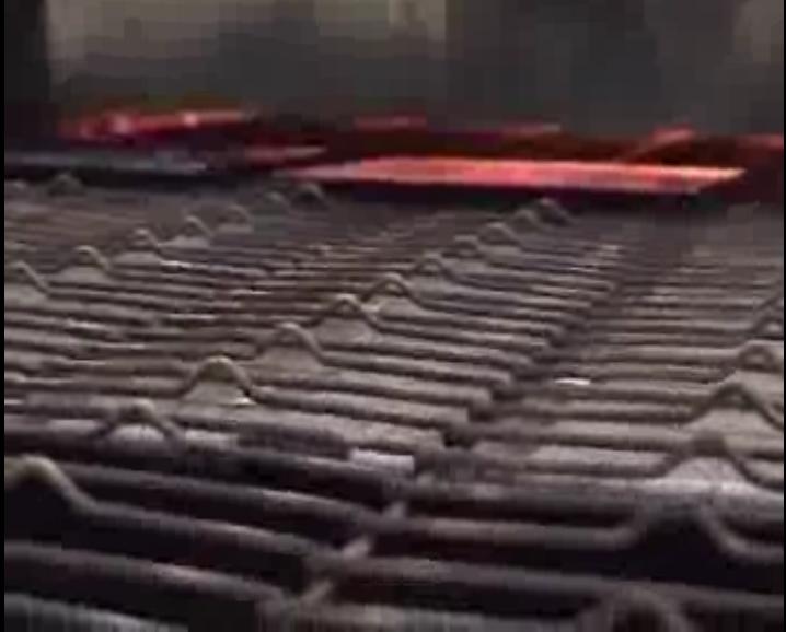
 - Over-firing causes the metal to diffuse deep into the semiconductor and across the junction - Results in a shunt: alternate pathway so")
29 Firing Metal Contacts under-fired contact correctly fired contact over-fired contact - Metal makes poor contact with the semiconductor - Results in a large series resistance (carriers recombine as they try to cross from the semicondcutor to the metal) - Over-firing causes the metal to diffuse deep into the semiconductor and across the junction - Results in a shunt: alternate pathway so carriers can avoid traveling through the depletion region


30 Silicon Solar Cells The rear side contacts are also screen-printed and fired. Two approaches are often employed: Aluminum layer with Al/Ag strips to connect multiple cells together better, but more expensive Only Al/Ag grid (most typical for commercial cells) not as good, but cheaper
 that")
31 Silicon Solar Cells Why the full aluminum rear contact is best: surface passivation through formation of a back surface field Recall that the cell s surfaces are often significant sources of recombination Recall also that Al is a p-type dopant in silicon The full aluminum layer has the advantage of contributing a back surface field (ultra-high p- doped region near the rear surface) that prevents minority carriers in the p-type region (electrons) from flowing towards the rear surface and promotes their flow towards the p-n junction So the net effect of the full Al layer is that it helps to passivate the rear surface n-type silicon p-type silicon p+ -type silicon aluminum back contact
32 Learning Objectives: Contacts Describe the purpose of contacts, and the two main types of contacts used in the solar industry Describe what is meant by an ohmic and a Schottky contact, and the work function. Explain why we use large work function metals to make ohmic contacts to p-type semiconductors, and small work function metals to make ohmic contacts to n-type semiconductors Describe how contacts are typically incorporated into solar cells, and some common firing problems that can arise Describe how transparent conducting oxides work. That is, how are the both transparent and conducting at the same time?

33 Buried Contact Solar Cells A newer concept that demonstrates high efficiencies:

34 Buried Contact Solar Cells A high efficiency concept in which a laser is used to make a groove inside the silicon Copper is used instead of silver, and is plated into the grooves Allows for a large metal height-to-width aspect ratio, which enables a large volume of metal to be used for good charge extraction, without having a wide strip of metal on the surface Compare: shading losses can be as high as 10-15% with screen printed cells, and as low as 2-3% with buried contacts Technology developed at UNSW in 1984, sold to a number of companies including BP Solar, Solarex, Samsung,

35 Transparent Conducting Oxides We don t have too many materials that both conduct electricity and are optically transparent (most transparent things are insulators, like glass or diamond or quartz) But, there are some. These tend to be metal oxides that normally would be insulating, but are either intentionally or naturally doped resulting in conductivity Requirements for a TCO: High transmittance (>80%), band gap greater than > 380 nm to avoid absorbing light Resistivities around 10-4 W-cm To date, the industry standard is ITO (tin-doped indium oxide). It is expensive, since indium is rare ($800/kg), but is often used in our thin-film solar cells Some alternatives are aluminum-doped zinc oxide (often used in CIGS), indiumdoped cadmium oxide, antimony-doped tin oxide (sometimes used in CdTe) Can be growth as a thin film via metalorganic chemical vapor deposition Konarka, Organic Solar Cell

36 Transparent Conducting Oxides Electronic structure: Large E g (transparent) Doping-induced defect states near the CB edge. metal oxide (wide band gap semiconductor)


37 Transparent Conducting Oxides
 http://www.engadget.")
38 Transparent Conducting Oxides Sharp Corporation, solar panels for the Japanese market (6.8% efficient)
ET3034TUx High efficiency concepts of c- Si wafer based solar cells
 ET3034TUx - 4.4 - High efficiency concepts of c- Si wafer based solar cells In the previous block we have discussed various technological aspects on crystalline silicon wafer based PV technology. In this
The next thin-film PV technology we will discuss today is based on CIGS.
 ET3034TUx - 5.3 - CIGS PV Technology The next thin-film PV technology we will discuss today is based on CIGS. CIGS stands for copper indium gallium selenide sulfide. The typical CIGS alloys are heterogeneous
An advantage of thin-film silicon solar cells is that they can be deposited on glass substrates and flexible substrates.
 ET3034TUx - 5.2.1 - Thin film silicon PV technology 1 Last week we have discussed the dominant PV technology in the current market, the PV technology based on c-si wafers. Now we will discuss a different
PHYSICSOF SOLARCELLS. Jenny Nelson. Imperial College, UK. Imperial College Press ICP
 im- PHYSICSOF SOLARCELLS Jenny Nelson Imperial College, UK ICP Imperial College Press Contents Preface v Chapter 1 Introduction 1 1.1. Photons In, Electrons Out: The Photovoltaic Effect 1 1.2. Brief History
Photovoltaic Fundamentals, Technology and Practice Dr. Mohamed Fawzy Aboud Sustainable Energy Technologies center (SET)
") Photovoltaic Fundamentals, Technology and Practice Dr. Mohamed Fawzy Aboud Sustainable Energy Technologies center (SET) The Greenhouse Effect 270 ppm carbon dioxide (CO 2 ) in the atmosphere absorbs outgoing
Photovoltaic Fundamentals, Technology and Practice Dr. Mohamed Fawzy Aboud Sustainable Energy Technologies center (SET) The Greenhouse Effect 270 ppm carbon dioxide (CO 2 ) in the atmosphere absorbs outgoing
Materials, Electronics and Renewable Energy
 Materials, Electronics and Renewable Energy Neil Greenham ncg11@cam.ac.uk Inorganic semiconductor solar cells Current-Voltage characteristic for photovoltaic semiconductor electrodes light Must specify
DESIGN AND OPERATING PRINCIPLES OF III- V SOLAR CELLS
 DESIGN AND OPERATING PRINCIPLES OF III- V SOLAR CELLS ANTHONY MELECO CAPSTONE ADVISER: DR. IAN SELLERS TABLE OF CONTENTS Abstract... 3 Introduction... 3 Procedure... 4 Photomask... 4 Modeling... 5 IV curve...
Crystalline Silicon Solar Cells With Two Different Metals. Toshiyuki Sameshima*, Kazuya Kogure, and Masahiko Hasumi
 Crystalline Silicon Solar Cells With Two Different Metals Toshiyuki Sameshima*, Kazuya Kogure, and Masahiko Hasumi Tokyo University of Agriculture and Technology, 2-24-16 Naka-cho, Koganei, Tokyo 184-8588,
Slide 1. Slide 2. Slide 3. Chapter 19: Electronic Materials. Learning Objectives. Introduction
 Slide 1 Chapter 19: Electronic Materials 19-1 Slide 2 Learning Objectives 1. Ohm s law and electrical conductivity 2. Band structure of solids 3. Conductivity of metals and alloys 4. Semiconductors 5.
Polycrystalline CdS/CdTe solar cells
 Polycrystalline CdS/CdTe solar cells Al Compaan Distinguished University Professor of Physics, Emeritus (Lecture for Heben/Ellingson solar cells class) March 3, 2011 1 Absorption spectra of various semiconductors
162 Solar Energy. front contact (metal grid) serial connections (to the back contact of the next cell) p-type wafer back contact
 serial connections (to the back contact of the next cell) p-type wafer back contact") 162 Solar Energy serial connections (to the back contact of the next cell) front contact (metal grid) antireflective coating n + -type emitter p + -type layer p-type wafer back contact 200 μm Figure 12.8:
162 Solar Energy serial connections (to the back contact of the next cell) front contact (metal grid) antireflective coating n + -type emitter p + -type layer p-type wafer back contact 200 μm Figure 12.8:
13.4 Chalcogenide solar cells Chalcopyrite solar cells
 13. Thin-Film Solar Cells 201 Figure 13.19: The crystal structure of copper indium diselenide, a typical chalcopyrite. The colors indicate copper (red), selenium (yellow) and indium (blue). For copper
Semiconductor Devices
 Semiconductor Devices - 2014 Lecture Course Part of SS Module PY4P03 Dr. P. Stamenov School of Physics and CRANN, Trinity College, Dublin 2, Ireland Hilary Term, TCD 20 th of Jan 14 M-S and p-n Junctions
Figure 16.31: Two-dimensional representations of (a) a quartz crystal and (b) a quartz glass.
 a quartz crystal and (b) a quartz glass.") Figure 16.31: Two-dimensional representations of (a) a quartz crystal and (b) a quartz glass. Figure 16.28: The p orbitals (a) perpendicular to the plane of th carbon ring system in graphite can combine
Figure 16.31: Two-dimensional representations of (a) a quartz crystal and (b) a quartz glass. Figure 16.28: The p orbitals (a) perpendicular to the plane of th carbon ring system in graphite can combine
Chapter 7 FABRICATION OF CIGS THIN FILM SOLAR CELL DEVICE AND ITS CHARACTERIZATION
 Chapter 7 FABRICATION OF CIGS THIN FILM SOLAR CELL DEVICE AND ITS CHARACTERIZATION 7. FABRICATION OF CIGS THIN FILM SOLAR CELL DEVICE AND ITS CHARACTERIZATION The solar cell structure based on copper indium
Semiconductor Optical Communication Components and Devices Lecture 30: Lasers Reliability
 Semiconductor Optical Communication Components and Devices Lecture 30: Lasers Reliability Prof. Utpal Das Professor, Department of Electrical Engineering, Laser Technology Program, Indian Institute of
NanoMarkets. Markets for Indium-Based Materials in Photovoltaics Nano-405. Published September NanoMarkets, LC
 Markets for Indium-Based Materials in Photovoltaics Nano-405 Published September 2011 NanoMarkets, LC NanoMarkets, LC PO Box 3840 Glen Allen, VA 23058 Tel: 804-360-2967 Web: Chapter One: Introduction 1.1
Transparent oxides for selective contacts and passivation in heterojunction silicon solar cells
 Transparent oxides for selective contacts and passivation in heterojunction silicon solar cells Francesca Menchini Photovoltaic Technologies Laboratory, ENEA Casaccia LIMS 2018 17-18 maggio 2018 Outline
Solar cell technologies present and future
 Solar cell technologies present and future Joachim LUTHER, Armin ABERLE and Peter Wuerfel Solar Energy Research Institute of Singapore (SERIS) Nature Photonics Technology Conference, Tokyo, Japan 20 October
The Potential of Photovoltaics
 The Potential of Photovoltaics AIMCAL 2008 2008 Fall Conference Vacuum Web Coating Brent P. Nelson October 22, 2008 NREL is a national laboratory of the U.S. Department of Energy Office of Energy Efficiency
KGC SCIENTIFIC TYPES OF SOLAR CELL
 KGC SCIENTIFIC www.kgcscientific.com TYPES OF SOLAR CELL How Photovoltaic Cell Work When sunshine that contain photon strike the panel, semiconductor material will ionized Causing electron to break free
REAR SURFACE PASSIVATION OF INTERDIGITATED BACK CONTACT SILICON HETEROJUNCTION SOLAR CELL AND 2D SIMULATION STUDY
 REAR SURFACE PASSIVATION OF INTERDIGITATED BACK CONTACT SILICON HETEROJUNCTION SOLAR CELL AND 2D SIMULATION STUDY Meijun Lu 1,2, Ujjwal Das 1, Stuart Bowden 1, and Robert Birkmire 1,2 1 Institute of Energy
Thin film solar cells
 Thin film solar cells pn junction: a:si cells heterojunction cells: CIGS-based CdTe-based 1 Amorphous Si large concentration of defects N T >10 16 cm -3 ( dangling bonds D +, D -, D o ) passivation of
High Transmittance Ti doped ITO Transparent Conducting Layer Applying to UV-LED. Y. H. Lin and C. Y. Liu
 High Transmittance Ti doped ITO Transparent Conducting Layer Applying to UV-LED Y. H. Lin and C. Y. Liu Department of Chemical Engineering and Materials Engineering, National Central University, Jhongli,
SOLAR ENERGY. Approximately 120,000 TW of solar energy strikes the earth s surface, capturing only a fraction could supply all of our energy needs.
 SOLAR ENERGY Approximately 120,000 TW of solar energy strikes the earth s surface, capturing only a fraction could supply all of our energy needs. What is Photovoltaics? Photovoltaics is a high-technology
Grid-Tied PV System with Energy Optimization
 International Journal of Engineering Works Kambohwell Publisher Enterprises Vol. 4, Issue 10, PP. 184-189, October 2017 www.kwpublisher.com Grid-Tied PV System with Energy Optimization Maryam Shahjehan,
Most semiconductor devices contain at least one junction between p-type and n-type material. These p-n junctions are fundamental to the performance
 Ch. 5: p-n Junction Most semiconductor devices contain at least one junction between p-type and n-type material. These p-n junctions are fundamental to the performance of functions such as rectification,
Assignment Questions
 HIGH SPEED DEVICES AND CIRCUITS Assignment Questions 1) Why Silicon Semiconductors are widely used in the VLSI applications? Hint: Refer Video on Introduction to Basic Concepts 2) What are the parameters
Amorphous silicon / crystalline silicon heterojunction solar cell
 Workshop on "Physics for Renewable Energy" October 17-29, 2005 301/1679-9 "Amorphous Silicon / Cyrstalline Silicon Heterojunction Solar Cell" E. Centurioni CNR/IMM AREA Science Park - Bologna Italy Amorphous
Material Needs for Thin-Film and Concentrator Photovoltaic Modules
 Material Needs for Thin-Film and Concentrator Photovoltaic Modules NREL Sarah Kurtz CDMA Conference: Opportunities for Chemicals and Materials in Wind and Solar Energy December 4, 2009 Philadelphia, PA
Spotlight on Photovoltaics & Fuel Cells: A Web-based Study & Comparison (Teacher Notes)
") General Lesson Notes Electrochemistry is defined as the branch of chemistry that deals with oxidationreduction reactions that transfer electrons to form electrical energy rather than heat energy. An electrode
General Lesson Notes Electrochemistry is defined as the branch of chemistry that deals with oxidationreduction reactions that transfer electrons to form electrical energy rather than heat energy. An electrode
Fabrication and Layout
 Fabrication and Layout Kenneth Yun UC San Diego Adapted from EE271 notes, Stanford University Overview Semiconductor properties How chips are made Design rules for layout Reading Fabrication: W&E 3.1,
ECE 440 Lecture 27 : Equilibrium P-N Junctions I Class Outline:
 ECE 440 Lecture 27 : Equilibrium P-N Junctions I Class Outline: Fabrication of p-n junctions Contact Potential Things you should know when you leave Key Questions What are the necessary steps to fabricate
"Plasma CVD passivation; Key to high efficiency silicon solar cells",
 "Plasma CVD passivation; Key to high efficiency silicon solar cells", David Tanner Date: May 7, 2015 2012 GTAT Corporation. All rights reserved. Summary: Remarkable efficiency improvements of silicon solar
Amorphous Silicon Solar Cells
 The Birnie Group solar class and website were created with much-appreciated support from the NSF CRCD Program under grants 0203504 and 0509886. Continuing Support from the McLaren Endowment is also greatly
Processing of Semiconducting Materials Prof. Pallab Benerji Department of Materials Science Center Indian Institute of Technology, Kharagpur
 Processing of Semiconducting Materials Prof. Pallab Benerji Department of Materials Science Center Indian Institute of Technology, Kharagpur Lecture - 11 Compound Semiconductors (Refer Slide Time: 00:20)
Thin film silicon technology. Cosimo Gerardi 3SUN R&D Tech. Coordinator
 Thin film silicon technology Cosimo Gerardi 3SUN R&D Tech. Coordinator 1 Outline Why thin film Si? Advantages of Si thin film Si thin film vs. other thin film Hydrogenated amorphous silicon Energy gap
Organic Light-Emitting Diodes. By: Sanjay Tiwari
 Organic Light-Emitting Diodes By: Sanjay Tiwari Inorganic Vs. Organic Material Properties Limitations At Early Stage Organic materials have often proved to be unstable. Making reliable electrical contacts
Photovoltaics under concentrated sunlight
 Photovoltaics under concentrated sunlight April 2, 2013 The University of Toledo, Department of Physics and Astronomy Principles and Varieties of Solar Energy (PHYS 4400) Reading assignment: Sections 9.4
Semiconductor Very Basics
 Semiconductor Very Basics Material (mostly) from Semiconductor Devices, Physics & Technology, S.M. Sze, John Wiley & Sons Semiconductor Detectors, H. Spieler (notes) July 3, 2003 Conductors, Semi-Conductors,
PV System Components
 PV System Components PV modules each containing many PC cells. Connected in series or parallel arrays. Charge Controllers Optimally charges a storage battery for an off grid system, or Grid tie Inverters
Solar and Wind Energy
 Jerry Hudgins Solar and Wind Energy Department of Electrical Engineering 1 Average Irradiation Data (Annual) from Solarex. The units on the map are in kwh/m 2 /day and represent the minimum case values
Lecture 0: Introduction
 Lecture 0: Introduction Introduction Integrated circuits: many transistors on one chip. Very Large Scale Integration (VLSI): bucketloads! Complementary Metal Oxide Semiconductor Fast, cheap, low power
ECE 541/ME 541 Microelectronic Fabrication Techniques
 ECE 541/ME 541 Microelectronic Fabrication Techniques MW 4:00-5:15 pm Metrology and Characterization Zheng Yang ERF 3017, email: yangzhen@uic.edu ECE541/ME541 Microelectronic Fabrication Techniques Page
Summary and Scope for further study
 Chapter 6 Summary and Scope for further study 6.1 Summary of the present study Transparent electronics is an emerging science and technology field concentrated on fabricating invisible electronic circuits
AMORPHOUS SILICON DIOXIDE LAYER FOR HIGH EFFICIENCY CRYSTALLINE SOLAR CELLS
 International Journal of Nanotechnology and Application (IJNA) ISSN(P): 2277-4777; ISSN(E): 2278-9391 Vol. 6, Issue 5, Dec 2016, 1-6 TJPRC Pvt. Ltd. AMORPHOUS SILICON DIOXIDE LAYER FOR HIGH EFFICIENCY
Lecture 22: Integrated circuit fabrication
 Lecture 22: Integrated circuit fabrication Contents 1 Introduction 1 2 Layering 4 3 Patterning 7 4 Doping 8 4.1 Thermal diffusion......................... 10 4.2 Ion implantation.........................
VLSI Technology Dr. Nandita Dasgupta Department of Electrical Engineering Indian Institute of Technology, Madras
 VLSI Technology Dr. Nandita Dasgupta Department of Electrical Engineering Indian Institute of Technology, Madras Lecture - 32 IC BJT - From junction isolation to LOCOS So, by now, we have completed all
Laser-Crystallised Thin-Film Polycrystalline Silicon Solar Cells. Jonathon Dore SPREE Research Seminar - 27th June, 2013
 Laser-Crystallised Thin-Film Polycrystalline Silicon Solar Cells Jonathon Dore SPREE Research Seminar - 27th June, 2013 Contents Introduction motivation for thin-film Thin-film PV technologies Diode laser
Optical Inspection for the Field of Thin-Film Solar
 Top quality for the photovoltaic industry Optical Inspection for the Field of Thin-Film Solar Thin-film solar cells are playing an increasingly important role in the photovoltaic industry. Even though
CMOS VLSI Design. Introduction. All materials are from the textbook Weste and Harris, 3 rd Edition CMOS VLSI DESIGN. Introduction
 CMOS VLSI Design Introduction ll materials are from the textbook Weste and Harris, 3 rd Edition CMOS VLSI DESIGN Introduction Chapter previews the entire field, subsequent chapters elaborate on specific
Nanoparticle Solar Cells
 Nanoparticle Solar Cells ECG653 Project Report submitted by Sandeep Sangaraju (sangaraj@unlv.nevada.edu), Fall 2008 1. Introduction: Solar cells are the most promising product in future. These can be of
Introduction. 1.1 Solar energy
 1 Introduction This chapter provides a general background on solar cells. In particular, the necessity of developing thin-film silicon tandem solar cells is discussed. The working principles of two different
Photovoltaics Outlook for Minnesota
 Photovoltaics Outlook for Minnesota Saving dollars, not polar bears Steve Campbell scampbell@umn.edu University of Minnesota Department of Electrical and Computer Engineering Outline Why solar? Solar technologies
Photonic Drying Pulsed Light as a low Temperature Sintering Process
 Photonic Drying Pulsed Light as a low Temperature Sintering Process Lou Panico Xenon Corporation W E S T E R N M I C H I G A N U N I V E R S I T Y PRESENTATION OVERVIEW What is Printed Electronics Materials
School of Photovoltaic and Renewable Energy Engineering
 School of Photovoltaic and Renewable Energy Engineering Silicon PV Education, Research and Industry in Australia R. Corkish, Head of School r.corkish@unsw.edu.au www.pv.unsw.edu.au Photo: K. McLean Context:
AN ABSTRACT OF THE THESIS OF. Benjamin E. Waters for the degree of Master of Science in
 AN ABSTRACT OF THE THESIS OF Benjamin E. Waters for the degree of Master of Science in Electrical and Computer Engineering presented on July 2, 2012. Title: Physical Vapor Deposition of Novel Thin-Film
Basics of Solar Photovoltaics. Photovoltaics (PV) Lecture-21
 Lecture-21") Lecture-21 Basics of Solar Photovoltaics Photovoltaics (PV) Photovoltaics (PV) comprise the technology to convert sunlight directly into electricity. The term photo means light and voltaic, electricity.
Lecture-21 Basics of Solar Photovoltaics Photovoltaics (PV) Photovoltaics (PV) comprise the technology to convert sunlight directly into electricity. The term photo means light and voltaic, electricity.
Passivation of SiO 2 /Si Interfaces Using High-Pressure-H 2 O-Vapor Heating
 Jpn. J. Appl. Phys. Vol. 39 (2000) pp. 2492 2496 Part, No. 5A, May 2000 c 2000 The Japan Society of Applied Physics Passivation of O 2 / Interfaces Using High-Pressure-H 2 O-Vapor Heating Keiji SAKAMOTO
HOMEWORK 4 and 5. March 15, Homework is due on Monday March 30, 2009 in Class. Answer the following questions from the Course Textbook:
 HOMEWORK 4 and 5 March 15, 2009 Homework is due on Monday March 30, 2009 in Class. Chapter 7 Answer the following questions from the Course Textbook: 7.2, 7.3, 7.4, 7.5, 7.6*, 7.7, 7.9*, 7.10*, 7.16, 7.17*,
VLSI. Lecture 1. Jaeyong Chung System-on-Chips (SoC) Laboratory Incheon National University. Based on slides of David Money Harris
 Laboratory Incheon National University. Based on slides of David Money Harris") VLSI Lecture 1 Jaeyong Chung System-on-Chips (SoC) Laboratory Incheon National University Based on slides of David Money Harris Goals of This Course Learn the principles of VLSI design Learn to design
VLSI Lecture 1 Jaeyong Chung System-on-Chips (SoC) Laboratory Incheon National University Based on slides of David Money Harris Goals of This Course Learn the principles of VLSI design Learn to design
Avalanche Breakdown (Reverse biased PN junction)
") Deviation from the Ideal Diode Ideal diode I The mechanism for breakdown 1. Avalanching 2. Zener Process -V BR -Io generation of carriers in the depletion region -I measured Real diode V A Ideal diode
Deviation from the Ideal Diode Ideal diode I The mechanism for breakdown 1. Avalanching 2. Zener Process -V BR -Io generation of carriers in the depletion region -I measured Real diode V A Ideal diode
EELE408 Photovoltaics Lecture 18 Photovoltaic Arrays & Modules
 EELE08 Photovoltaics Lecture 18 Photovoltaic Arrays & Modules Dr. Todd J. Kaiser tjkaiser@ece.montana.edu Department of Electrical and Computer Engineering Montana State University - Bozeman Photovoltaic
TOWARD MEMS!Instructor: Riadh W. Y. Habash
 TOWARD MEMS!Instructor: Riadh W. Y. Habash Students are presented with aspects of general production and manufacturing of integrated circuit (IC) products to enable them to better liaise with and participate
Solar Spectrum. -Black body radiation. Light bulb 3000 K Red->Yellow->White Surface of Sun 6000 K
 Solar Spectrum 1 Solar Spectrum -Black body radiation Light bulb 3000 K Red->Yellow->White Surface of Sun 6000 K 2 Solar Spectrum -Black body radiation Light bulb 3000 K Red->Yellow->White Surface of Sun
Renewable Energy CHEM REBECCA SCHEIDT
 Renewable Energy CHEM20204 2018.3.20 REBECCA SCHEIDT Energy Consumption 1 Energy Consumption U.S. Energy Consumption in 2016 by Source Wind, 2.2% Hydro, 2.5% Biomass, 4.9% Nuclear, 8.6% Coal, 14.6% Solar,
Interface potential measurement with electron spectroscopic method
 Journal of Surface Analysis Vol.13 No. 2 (2006) pp. 185-189 Interface potential measurement with electron spectroscopic method Michiko Yoshitake * and Weijie Song National Research Institute for Materials
Schottky-barrier and MIS solar cells
 Schottky-barrier and MIS solar cells (Metal-Insulator- Semiconductor) Steve Byrnes NSE 290 Final Presentation December 1, 2008 Outline Background on Schottky barriers Dark and light I-V curves, and effect
Crystalline Silicon Solar Cells Future Directions. Stuart Bowden BAPVC January Stuart Bowden BAPVC January 12,
 Crystalline Silicon Solar Cells Future Directions Stuart Bowden BAPVC January 2011 Stuart Bowden BAPVC January 12, 2011 1 Stuart Bowden Co-Director of Solar Power Labs at ASU Work relevant to BAPVC: Pilot
Lab IV: Electrical Properties
 Lab IV: Electrical Properties Study Questions 1. How would the electrical conductivity of the following vary with temperature: (a) ionic solids; (b) semiconductors; (c) metals? Briefly explain your answer.
Amorphous silicon thin film solar cells
 Amorphous silicon thin film solar cells c-si a-si large concentration of intrinsic defects N T >10 16 cm -3 ( dangling bonds D +, D -, D o ) doping more difficult, e.g. if we increase a number of free
Roll to Roll Flexible Microgroove Based Photovoltaics. John Topping Chief Scientist Big Solar Limited
 Roll to Roll Flexible Microgroove Based Photovoltaics John Topping Chief Scientist Big Solar Limited Big Solar Limited, Washington Business Centre 2 Turbine Way, Sunderland SR5 3NZ Email: John@powerroll.solar
EE 330 Lecture 9. IC Fabrication Technology Part 2
 EE 330 Lecture 9 IC Fabrication Technology Part 2 Quiz 8 A 2m silicon crystal is cut into wafers using a wire saw. If the wire diameter is 220um and the wafer thickness is 350um, how many wafers will this
NanoMarkets. Emerging Markets for non-ito Transparent Conductive Oxides Nano-413. Published August NanoMarkets, LC
 Emerging Markets for non-ito Transparent Conductive Oxides Nano-413 Published August 2011 NanoMarkets, LC NanoMarkets, LC PO Box 3840 Glen Allen, VA 23058 Tel: 804-360-2967 Web: Chapter One: Introduction
Energy-efficient glazing
 Energy-efficient glazing Low-E solar reflective coatings Float glass is traditionally used in the building and automotive industries to provide both clear and tinted transparent barriers to the elements.
1 Introduction 1.1 Solar energy worldwide
 1 Introduction 1.1 Solar energy worldwide Solar energy, the earth s source of life, has an enormous potential to also become earth s inexhaustible and clean energy/electricity source. Each year the earth
EXPERIMENTAL STUDIES Of NEW GaAs METAL=INSULATOR=p-n þ SWITCHES USING LOW TEMPERATURE OXIDE
 Active and Passive Elec. Comp., 2002, Vol. 25, pp. 233 237 EXPERIMENTAL STUDIES Of NEW GaAs METAL=INSULATOR=p-n þ SWITCHES USING LOW TEMPERATURE OXIDE K. F. YARN* Far East College, Department of Electrical
Silicon Epitaxial CVD Want to create very sharp PN boundary grow one type layer on other in single crystal form High dopant layers on low dopant
 Silicon Epitaxial CVD Want to create very sharp PN boundary grow one type layer on other in single crystal form High dopant layers on low dopant substrate Creates latch up protection for CMOS Buried Epi
Semiconductor Device Fabrication
 5 May 2003 Review Homework 6 Semiconductor Device Fabrication William Shockley, 1945 The network before the internet Bell Labs established a group to develop a semiconductor replacement for the vacuum
High Speed Devices and Circuits Prof K. N. Bhat Department of Electrical Engineering Indian Institute of Technology, Madras
 High Speed Devices and Circuits Prof K. N. Bhat Department of Electrical Engineering Indian Institute of Technology, Madras Lecture 4 Ternary Compound Semiconductors and their Applications Last time we
Current Gain Dependence on Subcollector and Etch-Stop Doping in InGaP/GaAs HBTs
 IEEE TRANSACTIONS ON ELECTRON DEVICES, VOL. 48, NO. 5, MAY 2001 835 Current Gain Dependence on Subcollector and Etch-Stop Doping in InGaP/GaAs HBTs Theodore Chung, Seth R. Bank, John Epple, and Kuang-Chien
Solar Power. Technical Aspects and Environmental Impacts. 6 th March 2011 Sustainable Energy Options (UAU212F) - University of Iceland
 - University of Iceland") Solar Power Technical Aspects and Environmental Impacts 1 Solar Power 1. Introduction 2. Passive Solar Energy utilization 3. Solar Thermal Heat Utilization 4. Solar thermal power plants 5. Photovoltaic
Solar Power Technical Aspects and Environmental Impacts 1 Solar Power 1. Introduction 2. Passive Solar Energy utilization 3. Solar Thermal Heat Utilization 4. Solar thermal power plants 5. Photovoltaic
Ion Implantation Most modern devices doped using ion implanters Ionize gas sources (single +, 2+ or 3+ ionization) Accelerate dopant ions to very
 Accelerate dopant ions to very") Ion Implantation Most modern devices doped using ion implanters Ionize gas sources (single +, 2+ or 3+ ionization) Accelerate dopant ions to very high voltages (10-600 KeV) Use analyzer to selection charge/mass
Ion Implantation Most modern devices doped using ion implanters Ionize gas sources (single +, 2+ or 3+ ionization) Accelerate dopant ions to very high voltages (10-600 KeV) Use analyzer to selection charge/mass
M. Hasumi, J. Takenezawa, Y. Kanda, T. Nagao and T. Sameshima
 Proceedings of 6th Thin Film Materials & Devices Meeting November 2-3, 2009, Kyoto, Japan http://www.tfmd.jp/ Characterization of SiO x /Si Interface Properties by Photo Induced Carrier Microwave Absorption
Thermal Evaporation. Theory
 Thermal Evaporation Theory 1. Introduction Procedures for depositing films are a very important set of processes since all of the layers above the surface of the wafer must be deposited. We can classify
Lecture 7 Solar Energy Solar Resource Physical principles of solar conversion (elec.) Solar conversion technologies Photovoltaics
 Solar conversion technologies Photovoltaics") Lecture 7 Solar Energy Solar Resource Physical principles of solar conversion (elec.) Solar conversion technologies Photovoltaics Principles, technologies, systems, costs, markets Assessing PV output Global
Lecture 7 Solar Energy Solar Resource Physical principles of solar conversion (elec.) Solar conversion technologies Photovoltaics Principles, technologies, systems, costs, markets Assessing PV output Global
Chapter 18: Electrical Properties
 Chapter 18: Electrical Properties ISSUES TO ADDRESS... How are electrical conductance and resistance characterized? What are the physical phenomena that distinguish conductors, semiconductors, and insulators?
Topics Relevant to CdTe Thin Film Solar Cells
 Topics Relevant to CdTe Thin Film Solar Cells March 13, 2012 The University of Toledo, Department of Physics and Astronomy SSARE, PVIC Principles and Varieties of Solar Energy (PHYS 4400) and Fundamentals
TWO-DIMENSIONAL MODELING OF EWT MULTICRYSTALLINE SILICON SOLAR CELLS AND COMPARISON WITH THE IBC SOLAR CELL
 TWO-DIMENSIONAL MODELING OF EWT MULTICRYSTALLINE SILICON SOLAR CELLS AND COMPARISON WITH THE IBC SOLAR CELL Mohamed M. Hilali, Peter Hacke, and James M. Gee Advent Solar, Inc. 8 Bradbury Drive S.E, Suite,
Crystalline Silicon Technologies
 Crystalline Silicon Technologies in this web service in this web service Mater. Res. Soc. Symp. Proc. Vol. 1210 2010 Materials Research Society 1210-Q01-01 Hydrogen Passivation of Defects in Crystalline
Schottky Tunnel Contacts for Efficient Coupling of Photovoltaics and Catalysts
 Schottky Tunnel Contacts for Efficient Coupling of Photovoltaics and Catalysts Christopher E. D. Chidsey Department of Chemistry Stanford University Collaborators: Paul C. McIntyre, Y.W. Chen, J.D. Prange,
THREE TERMINAL SI-SI:GE MONOLITIC TANDEM SOLAR CELLS. Lu Wang
 THREE TERMINAL SI-SI:GE MONOLITIC TANDEM SOLAR CELLS by Lu Wang A thesis submitted to the Faculty of the University of Delaware in partial fulfillment of the requirements for the degree of Master of Science
The Effect of Annealing on Resistivity Measurements of TiSi 2 and TiN Using the collinear Four Point Probe Technique
 The Effect of Annealing on Resistivity Measurements of TiSi 2 and TiN Using the collinear Four Point Probe Technique Eman Mousa Alhajji North Carolina State University Department of Materials Science and
Deviation from the Ideal Diode. Ideal diode equation. I The mechanism for breakdown 1. Avalanching 2. Zener Process. Ideal diode
 Deviation from the Ideal Diode Ideal diode I The mechanism for breakdown 1. Avalanching 2. Zener Process -V BR -Io generation of carriers in the depletion region -I measured Real diode V A Ideal diode
Surface Preparation Challenges in Crystalline Silicon Photovoltaic Manufacturing
 Surface Preparation Challenges in Crystalline Silicon Photovoltaic Manufacturing Kristopher Davis 1,3, Andrew C. Rudack 2,3, Winston Schoenfeld 1,3 Hubert Seigneur 1,3, Joe Walters 1,3, Linda Wilson 2,3
Lecture 6. Monocrystalline Solar Cells
 Lecture 6 Monocrystalline Solar Cells References: 1. Physics of Solar Cells. Jenny Nelson. Imperial College Press, 2003. 2. Photovoltaic Materials, Series on Properties of Semiconductor Materials, Vol.1,
PROCESS FLOW AN INSIGHT INTO CMOS FABRICATION PROCESS
 Contents: VI Sem ECE 06EC63: Analog and Mixed Mode VLSI Design PROCESS FLOW AN INSIGHT INTO CMOS FABRICATION PROCESS 1. Introduction 2. CMOS Fabrication 3. Simplified View of Fabrication Process 3.1 Alternative
Silver Diffusion Bonding and Layer Transfer of Lithium Niobate to Silicon
 Chapter 5 Silver Diffusion Bonding and Layer Transfer of Lithium Niobate to Silicon 5.1 Introduction In this chapter, we discuss a method of metallic bonding between two deposited silver layers. A diffusion
Design of very thin CdTe Solar Cells with high efficiency
 Available online at www.sciencedirect.com ScienceDirect Energy Procedia 57 (2014 ) 3051 3057 2013 ISES Solar World Congress Design of very thin CdTe Solar Cells with high efficiency Arturo Morales-Acevedo*