FORMING-FREE NITROGEN-DOPED ALUMINUM OXIDE RESISTIVE RANDOM ACCESS MEMORY GROWN BY ATOMIC LAYER DEPOSITION TECHNIQUE A DISSERTATION
|
|
|
- Caroline Briggs
- 6 years ago
- Views:
Transcription
1 FORMING-FREE NITROGEN-DOPED ALUMINUM OXIDE RESISTIVE RANDOM ACCESS MEMORY GROWN BY ATOMIC LAYER DEPOSITION TECHNIQUE A DISSERTATION SUBMITTED TO THE DEPARTMENT OF ELECTRICAL ENGINEERING AND THE COMMITTEE ON GRADUATE STUDIES OF STANFORD UNIVERSITY IN PARTIAL FULFILLMENT OF THE REQUIREMENTS FOR THE DEGREE OF DOCTOR OF PHILOSOPHY Sung Il Park November 2013
2 2013 by Sung Il Park. All Rights Reserved. Re-distributed by Stanford University under license with the author. This work is licensed under a Creative Commons Attribution- Noncommercial 3.0 United States License. This dissertation is online at: ii
3 I certify that I have read this dissertation and that, in my opinion, it is fully adequate in scope and quality as a dissertation for the degree of Doctor of Philosophy. S Simon Wong, Primary Adviser I certify that I have read this dissertation and that, in my opinion, it is fully adequate in scope and quality as a dissertation for the degree of Doctor of Philosophy. Yoshio Nishi I certify that I have read this dissertation and that, in my opinion, it is fully adequate in scope and quality as a dissertation for the degree of Doctor of Philosophy. Philip Wong Approved for the Stanford University Committee on Graduate Studies. Patricia J. Gumport, Vice Provost for Graduate Education This signature page was generated electronically upon submission of this dissertation in electronic format. An original signed hard copy of the signature page is on file in University Archives. iii
4 Abstract As flash memory devices begin to scale into the sub-20nm lithographical regime, scaling is becoming a challenge because of high electric field requirements for a high programming or erase voltage and rigid leakage requirements for long term storage. In addition, the flash memory design has been based on a two-dimensional approach and density of integration is reaching its limits. To tackle these issues, many candidates for next generation non-volatile memory such as phase change random access memory (PCRAM), STT-magnetic random access memory (STT-RAM), ferroelectric random access memory (FeRAM), and resistive random access memory (RRAM) have been introduced and studied. Among these devices concepts RRAM is a prime candidate because of its unique characteristics. In order for RRAM technology to be adopted for manufacturing, the technology must meet the following requirements. First, the direct integration of metal oxide RRAM on MOSFET should be feasible and RRAM cells must be compatible with the standard CMOS process. Second, it must not require a high forming voltage and it should be programmed with an applied current below sub-ua at high data rates for many switching cycles. Finally, RRAM cells must be feasible for storing multiple bits. We demonstrated nitrogen-doped aluminum oxide RRAM that meets the requirements and the RRAM cell was deposited by a physical vapor deposition technique. However, it has been found that more uniform films can be deposited by an atomic layer deposition technique, and we believe that more uniform films are responsible for uniform switching characteristics. That is the motivation of this dissertation. We have demonstrated nitrogen-doped aluminum oxide RRAM grown by an atomic layer deposition technique and have monolithically integrated such RRAM cells on top of selection transistors to achieve accurate control of the voltage and current waveforms for programming. We have studied the control of the on-and off-behavior of the RRAM cell by gathering the statistics on the turn-on and turn-off voltage, current and resistance as a function of the bias voltages and the limiting current on the selection MOSFET, and thereby evaluated the feasibility of multi-level programming, reliability, endurance and retention of nitrogen-doped aluminum oxide RRAM. Through this study, novel multi-bit programming strategies were investigated through accurate control of the programming waveform. The data collected iv
5 through this extensive study will provide important information on the viability of metal-oxide films for future generation stand-alone and embedded non-volatile memory applications. The demonstration of multi-level programming will greatly extend the scalability of RRAM. The evaluation methodology we develop can be extended to other resistance-change films. v
6 Acknowledgments I would like to express my thanks to my academic advisor, Professor S.Simon Wong. During my graduate study, he has been academically and financially supportive. An important lesson that I have learned from him is knowing the difference between science and engineering; science asks how nature works and engineering asks how nature can be used. He always asked his students to focus on practical issues and the lesson will be a long term asset for my research journey. Also, I would like to extend my thanks to Professor Yoshio Nishi and Professor H.S. Philip Wong. They gave valuable feedback to my thesis and without them my thesis could not be finished. Next gratitude is reserved for our group members, Wanki Kim, Zhiping Zhang, Jeongha Park, Stanley Yeh, Chaohao Wang, Young-yang Liew, and Alex Omid-zohor. Wanki, Zhiping, and myself worked together to develop RRAM stacks and integrate RRAM cells on top of MOSFET, and I cannot imagine the end of my Ph.D study without them. Next, I want to thank June Wang who is our group secretary, Jim Mcvittee who is in charge of AJA sputtering machine, and Michelle Rinconn who is in charge of Fiji atomic layer deposition tool. When the machine had a problem or even was broken, they always took prompt actions to fix the problem. Next, I am deeply indebted to many friends at Stanford University for their support. Last but not least, I really thank my family. My depth of gratitude is too great to express in words. My parent raised me by sacrificing their life, and my lovely wife, Areum Han, has supported my study by taking care of our lovely kids, Hans and Yoon. vi
7 Table of Contents Abstract... iv Acknowledgments... vi List of Tables... ix List of Illustrations... x Chapter 1: Introduction Resistive Random Access Memory (RRAM) technology Basic operations of RRAM Introduction of nitrogen-doped aluminum oxide RRAM grown by PVD Atomic Layer Deposition Vs. Physical Vapor deposition Introduction of RRAM grown by ALD Overview of dissertation Chapter 2: Investigation of RRAM stacks TiN electrode for nitrogen-doped AlO x RRAM Aluminum nitride grown by ALD Incorporation of nitrogen into aluminum oxide AlO x N y composite material AlN grown on Al 2 O AlN grown on TiN electrode Al 2 O 3 / AlN with TiN electrode XPS analysis for nitrogen-doped aluminum oxide RRAM Chapter 3: Optimization of Al 2 O 3 / AlN with TiN electrode Switching characteristics in terms of AlN thickness Switching characteristics in terms of Al 2 O 3 thickness Switching characteristics dependency on annealing time Chapter 4: Fabrication of N-doped AlO X RRAM grown by ALD 1T1R system Introduction of selection transistors vii
8 4.2. Integration of N-doped AlO x RRAM with CMOS Description of 1Transistor 1RRAM structure Chapter 5: Electrical switching characteristics of N-doped AlO X RRAM grown by ALD Measurement setup for 1T1R structure I-V switching characteristics Programming voltage distribution Set/reset current versus on resistance Linear and non-linear I-V characteristics of HRS and various LRS Conduction mechanism in ALD N-AlO x RRAM Reliability characteristics of ALD N-AlO x RRAM Retention results at 120 C Read disturb characteristics Endurance switching characteristics Chapter 6: Incorporation of nitrogen into Al 2 O 3 films Role of nitrogen for resistive switching characteristics Electrical switching characteristics in terms of nitrogen concentration Set / reset current versus on-resistance Extrapolated energy barrier Endurance characteristics Chapter 7: Conclusion Summary Recommendation for future works Bibliography viii
9 List of Tables Number Page Table 2.1: Summary of ALD TiN properties Table 3.1: Summary of switching parameters versus AlN thickness Table 3.2: Summary of switching characteristics versus Al 2 O 3 thickness Table 3.3: Dependency on annealing time of switching characteristics Table 4.1: Description of NMOS transistors with different sizes.w and L indicate channel width and length of selection transistors, respectively Table 4.2: RRAM cells of different sizes. The numbering corresponds to those shown in Figure 4.5 (b) Table 6.1: N-AlO x with various nitrogen concentrations Table 6.2: Summary of extrapolated trap barrier height for HRS Table 6.3: Summary of extrapolated trap barrier height for each LRS Table 6.4: Summary of endurance characteristics ix
10 List of Illustrations Number Page Figure 1.1: Scaling trend of NAND flash technology [1] Figure 1.2: Basic I-V characteristics of RRAM; (a) unipolar operations with a forming process (b) bipolar operations with a forming process[17] Figure 1.3: Nitrogen-doped aluminum oxide RRAM deposited by the PVD system;(a) crosssectional view of a RRAM cell, (b) basic switching characteristics, and (c) retention characteristics of N-AlO x RRAM cells[21] Figure 1.4: Illustration of deposition cycles consisting of 4 steps in the atomic layer deposition system; (a) exposure of metal precursors, (b) evacuation of reactants or any by-products, (c) exposure of H 2 O, and (d) purging out of reactants or byproducts. (e) Illustration of Al 2 O 3 layer grown on a silicon substrate after one deposition cycle is reached[22] Figure 1.5: Illustration of deposition processes in the physical vapor deposition system[23] Figure 1.6: Summary of characteristics of films deposited by several deposition techniques[22] Figure 1.7: Switching characteristics of hafnium-based RRAM deposited by an atomic layer deposition technique. (a) Illustration of a forming process, (b) basic I-V characteristics, (c) endurance characteristics, and (d) retention characteristics of HfO X RRAM[24] Figure 2.1: AFM picture of TiN films deposited by ALD Figure 2.2: Atomic profiles of AlN grown on TiN layer Figure 2.3: Cross-sectional view of layered aluminum oxynitride (AlO X N Y ) Figure 2.4: Illustration of a set process of AlO X N Y Figure 2.5: Atomic profiles of alternating layers of Al 2 O 3 and AlN Figure 2.6: Cross-sectional view of AlN / Al 2 O 3 stacks Figure 2.7: Illustration of a set process of AlN / Al 2 O 3 stacks Figure 2.8: Atomic profiles of (a) as-deposited AlN / Al 2 O 3 stacks and (b) annealed AlN / Al 2 O 3 stacks Figure 2.9: Atomic profiles of (a) AlN grown on top of SiO 2 and (b) AlN grown on top of HfO Figure 2.10: Process flow of nitrogen-doped aluminum oxide RRAM stacks (50 um X 50 um); (a) cross-sectional view of N-AlO x, (b) patterning for the bottom electrode, (c) patterning for the top electrode, and (d) after annealing at 400 C for 15 minutes x
11 Figure 2.11: Illustration of forming free switching behavior Figure 2.12: Basic I-V characteristics of nitrogen-doped aluminum oxide RRAM with TiN electrodes Figure 2.13: Atomic profiles of (a) as-deposited stacks and (b) annealed stacks at 400 C for 30 minutes Figure 2.14: Bonding information;(a) Al2p, (b) O1s, and (c) N1s Figure 2.15: The peak signals of N1s[33] Figure 4.1: (a) I D -V D and (b) I D -V G characteristics of a 10 um / 1 um NMOS transistor Figure 4.2: Illustration of the process flow for integration of N-AlO x on top of selection transistors Figure 4.3: (a) Cross-sectional view of RRAM stacks, (b) top view of 1T1R structure, and (c) cross-sectional schematic of 1T1R structure Figure 4.4: Cross-sectional view of RRAM stacks that were deposited in a via region Figure 4.5: (a) Test chip snapshot and (b) an enlarged view of 1T1R RRAM area Figure 5.1: Illustration of measurement set-up for (a) set and (b) reset switching Figure 5.2: I-V switching characteristics of ALD N-AlO x RRAM Figure 5.3: Illustration of set switching behaviors showing no forming process Figure 5.4: Set switching behavior as a function of the gate bias of selection transistors for (a) ALD N-AlO x 1T1R structure and (b) PVD N-AlO x 1T1R structure, respectively Figure 5.5: Distributions of (a) set and (b) reset voltages of N-AlO x. The set and reset current are limited to 300nA and 1uA, respectively Figure 5.6: (a) Set current versus on-resistance and (b) reset current versus on-resistance Figure 5.7: Plot of natural log of current versus square root of voltage for HRS and various LRS Figure 5.8: Dependency on temperature of HRS and various LRS Figure 5.9: I-V relationship of (a) HRS and (b) LRS at various temperatures Figure 5.10: Temperature dependence of HRS and LRS Figure 5.11: Illustration of curve-fitting for the Frenkel-Poole emission model Figure 5.12: Illustration of curve-fitting for the Schottky emission model Figure 5.13: Energy band diagram of (a) after an annealing process and (b) after a set process Figure 5.14: Macroscopic conduction model of ALD N-AlO x RRAM xi
12 Figure 5.15: Retention results of the high resistance state and various resistance states at 120 C Figure 5.16: Read disturb characteristics of various resistance states Figure 5.17: Endurance characteristics of (a) without using smart programming and (b) with using smart programming for N-AlO x Figure 6.1: (a) Set current versus on-resistance and (b) reset current versus on-resistance for Al 2 O 3, 3 % N-AlO x, and 6 % N-AlO x, respectively Figure 6.2: (a) Set current versus on-resistance and (b) reset current versus on-resistance for 6 % N-AlO x, 12 % N-AlO x, and AlN, respectively Figure 6.3: Fitting results for the Frenkel-Poole emission model of HRS Figure 6.4: Fitting results for the Frenkel-Poole emission model of 1MΩ LRS Figure 6.5: Pulse endurance characteristics of (a) Al 2 O 3, (b) 3 % N-AlO x, (c) 6 % N-AlO x, (d) 12 % N-AlO x, and (e) AlN xii

13 Chapter 1: Introduction 1.1. Resistive Random Access Memory (RRAM) technology In order to satisfy society's seemingly insatiable demand for new computers, video games, and smart phones, Moore's law dictates that a new generation of technology be introduced every two years or so. Many studies pertaining to advanced technologies follow this guideline. The main reasons for scaling down the dimensions of logic devices are higher device density and better performance. Scaling allows more transistors to be integrated into a chip with the same dimensions, and integrated chips based on this new technology operate faster and consume less power. Figure 1.1: Scaling trend of NAND flash technology [1]. 1
14 However, silicon, which is the most important material in the semiconductor industry and the major reason why the semiconductor business has become successful, is reaching its physical limits. Thus, an integration density based on a two-dimensional approach, where transistors and passive components are placed in the same plane, is approaching its limit. From a structural point of view, traditional non-volatile memory structures such as NAND and NOR flash memory will be vulnerable to breakdown because a high programming voltage over 10 V is required as we scale down below 15 nm. In addition, a programming time of micro-second range for flash memory is not desirable for nano-second scale operation. To overcome these issues, many candidates such as Resistive Random Access Memory (RRAM)[2-4], Phase Change Random Access Memory (PCRAM)[5], Magnetic Random Access Memory (MRAM)[6], and Ferroelectric Random Access Memory (FeRAM)[7] have been introduced and extensively investigated. Among these candidates, the RRAM technology is the most promising non-volatile memory technology. The structure of RRAM is a simple metal-insulator-metal structure (MIM) that consists of a resistive dielectric material sandwiched between two metal electrodes. Operation of RRAM is also simple. Memory cells start in the high resistance state (HRS) which corresponds to logic 0 state. At about 2 V, it will be set to the low resistance state (LRS) associated with logic 1 state. That is, its state can be easily switched by applying low voltages. Compared with flash memory in which a high voltage over 10 V is required when switching the state of memory cells, the voltage required to switch the state of RRAM cells is low. Hence, no extra circuits such as a charge pump circuit is required to implement a high voltage, which simplifies the design of memory array. Simple MIM structure and operation of RRAM have triggered interest, and many candidate resistive dielectric materials based on oxides of nickel[8,9], titanium[10], hafnium[11], and aluminum[12] with different electrodes for the dielectric films have been introduced and extensively investigated. At an early stage, nickel oxide and titanium oxide based RRAM were studied and those RRAM cells showed moderate performances such as ua-range current levels[8-2
15 10]. Hafnium based RRAM showed low power operation and a fast programming cycle[11], but the RRAM requires a forming process by which a resistive switching behavior is facilitated. Recently, we demonstrated nitrogen-doped aluminum oxide (N-AlO X ) RRAM technology with very promising switching characteristics. This technology was based on the physical vapor deposition (PVD) system. Although the N-doped AlO X RRAM technology shows low power operation and fast switching cycles, the control and reproducibility of PVD is marginal. We have studied N-doped AlO X RRAM grown by an atomic layer deposition (ALD) technique to make the RRAM technology more consistent. It is well known that films grown by ALD outweigh films deposited by PVD in term of the step coverage and uniformity of films[13]. We believe that more uniform films guarantee more consistent switching characteristics which are desirable for the design of memory cell arrays, and this is why we started ALD work. Along with studies to improve performance by investigating materials, switching mechanisms such as the filament theory[14], the ion migration model[15], and the Schottky or Frenkel-Poole emission model[16] to understand what principle RRAM cells operate on and to identify how they change its state from HRS (LRS) to LRS (HRS) from a physical point of view have been proposed. The filament theory involves oxygen vacancies which is associated with LRS. When a current is passed through the filament, heat is released and the filament is broken [14]. The ion migration model explains that the migration of oxygen ions is responsible for resistive switching behaviors of RRAM. When ions are aligned in series or form a current path, the state of memory cells is LRS. When an opposite polarity bias is applied across memory cells, however, ions are repelled or the chain of ions are broken by the bias and this results in HRS[15]. Two common models such as the Schottky emission and Frenkel-Poole emission model explain rectifying conduction behavior in dielectric films. Both models have almost linear dependency between the natural log of current and the square root of voltage, and the energy barrier plays an important role in resistive switching characteristics[16]. In this dissertation, we studied two 3
16 models to understand resistive switching characteristics in the N-doped AlO X RRAM, and Chapter 5 will deal with this topic in detail. In order for a RRAM technology to be adopted for manufacturing, it must meet the following requirements. It must be compatible with the standard CMOS process and feasible for three dimensional stacking. It must be scalable to nm dimensions. In terms of programming performance, it must not require a high forming voltage. It should be programmed with a low current at high speed for many cycles. Finally, the RRAM cell must be capable of storing multiple bits reliably. For the rest of the dissertation, a RRAM with ALD nitrogen-doped aluminum oxide resistive dielectric that meets these requirements will be described Basic operations of RRAM (a) (b) Figure 1.2: Basic I-V characteristics of RRAM; (a) unipolar operations with a forming process (b) bipolar operations with a forming process[17]. One unique characteristic of RRAM is a high voltage forming process that initiates the programming functions[17-19]. Figure 1.2 shows the forming process and basic switching characteristics of RRAM[17]. As shown in Figure 1.2 (a), a RRAM cell starts in the high 4
17 resistance state. At about 2.5 V, memory cells will be set into the low resistance state with an applied current 0.5 ma. This low resistance state indicates that a memory cell store '1' bit. A voltage of 0.6 V will be applied to reset the memory cells back to the high resistance state associated with '0' bit. At the subsequent set cycle, RRAM cells can be set into the low resistance state with an applied voltage less than the forming voltage. Since this forming process is not reversible and complicates the design of selection devices and peripheral circuits, eliminating the forming process is desirable. For RRAM operations, there are two operation modes, one is unipolar switching mode and the other one is bipolar switching mode. As shown in Figure 1.2 (a), in unipolar mode the same polarity of bias will be applied across memory cells when we reset memory cells. In bipolar mode, a reverse polarity of bias will be applied across RRAM cells when we reset RRAM cells as shown in Figure 1.2 (b). In general, bipolar switching mode is more reliable than unipolar switching mode[20]. For this reason, we will focus on bipolar switching mode Introduction of nitrogen-doped aluminum oxide RRAM grown by PVD We demonstrated a forming free RRAM with nitrogen-doped aluminum oxide (N- AlO X ) resistance change film[21]. It is composed of 20 nm thick aluminum bottom electrode, 10 nm thick nitrogen-doped aluminum oxide resistive dielectric film, and 20 nm thick aluminum top electrode. These layers were deposited in-situ by a physical vapor deposition technique to prevent any contamination or oxidation along the interfaces. Figure 1.3 shows a cross-sectional view of the RRAM, basic switching characteristics, and retention characteristics. RRAM cells can be programmed or erased with an applied current below 50 na and no significant change of the resistances is observed for 10 5 seconds at 120 C. Recently, it has been found that more uniform and conformal films can be deposited by an atomic layer deposition technique. We believe that the uniformity of films affects the uniform switching characteristics. To achieve more uniform switching characteristics, we have developed N-AlO x film grown by ALD and integrated such 5

 (b) (c) Figure 1.")
 cross-sectional view of a RRAM cell, (b) basic")
18 RRAM on top of CMOS wafers. In the next section, we will introduce an ALD technique and discuss its advantages over a PVD technique. (a) (b) (c) Figure 1.3: Nitrogen-doped aluminum oxide RRAM deposited by the PVD system;(a) cross-sectional view of a RRAM cell, (b) basic switching characteristics, and (c) retention characteristics of N-AlO x RRAM cells[21]. 6
 (b) (c) (d)")

 exposure of metal")
 exposure of H 2 O, and")
 Illustration of Al 2 O 3 layer grown on")
19 1.4. Atomic Layer Deposition Vs. Physical Vapor deposition (a) (b) (c) (d) (e) Figure 1.4: Illustration of deposition cycles consisting of 4 steps in the atomic layer deposition system; (a) exposure of metal precursors, (b) evacuation of reactants or any by-products, (c) exposure of H 2 O, and (d) purging out of reactants or by-products. (e) Illustration of Al 2 O 3 layer grown on a silicon substrate after one deposition cycle is reached[22]. 7
![Atomic layer deposition (ALD) is a cyclic process that consists of an iterated sequence of deposition cycles[13,22].](/docs-images/71/65955706/images/20-0.jpg "Film thickness and properties are controlled at each cycle, and reproducible deposition of film composites by alternating layer composition is feasible.")
20 Atomic layer deposition (ALD) is a cyclic process that consists of an iterated sequence of deposition cycles[13,22]. Film thickness and properties are controlled at each cycle, and reproducible deposition of film composites by alternating layer composition is feasible. Because gas uniformity or flow does not affect layer growth, highly uniform and conformal films can be deposited. Figure 1.4 illustrates deposition cycles of the ALD system. In step 1, metal precursors are introduced into a chamber and react with atoms on the bottom layer. In the next step, precursors that do not have any bonding to the atom on the surface or any by-products are purged out of the chamber. In step 3, other precursors are delivered into the chamber and react with atoms in the layer deposited at step 1. Finally, un-reacted precursors and any by-products are evacuated. One of the most important requirements for the first step is the self-limitation of the precursor molecule absorption process. Usually, the ligands bonded to the metal atoms in the precursors, such as halogen or organic ligands, limit further absorption of the metal precursor by passivating the absorption sites after one monolayer is deposited. Figure 1.5: Illustration of deposition processes in the physical vapor deposition system[23]. 8

21 Figure 1.5 shows the deposition process in a PVD system based on sputtering. Highly energetic particles such as argon ions bombard the surface in the presence of high electric field. Then, atoms are ejected from the surface of a target material as a result of collision with highenergy particles according to Newton's law. Finally, the dislodged atoms or molecules condense on a substrate as a thin film. Figure 1.6: Summary of characteristics of films deposited by several deposition techniques[22]. Figure 1.6 compares the uniformity of films deposited by several deposition techniques and the film deposited by ALD shows better step coverage as expected. We believe that improved uniformity will result in uniform switching characteristics, which will be discussed in Chapter 5. 9
22 1.5. Introduction of RRAM grown by ALD Figure 1.7: Switching characteristics of hafnium-based RRAM deposited by an atomic layer deposition technique. (a) Illustration of a forming process, (b) basic I-V characteristics, (c) endurance characteristics, and (d) retention characteristics of HfO X RRAM[24]. As a replacement for silicon oxide, hafnium oxide has been extensively investigated due to its high dielectric constant and thermal stability. Such intensive studies about hafnium oxide have triggered research for RRAM applications[24]. Figure 1.7 shows basic I-V switching characteristics and reliability characteristics of hafnium oxide RRAM, and the hafnium oxide resistive dielectric film with TiN electrodes was grown by ALD. The RRAM cell requires a 10
23 forming process and the cell can be programmed or erased with an applied current of about 10 ua as shown in Figure 1.7 (a) & (b). Hafnium oxide RRAM cells are switchable over 10 3 switching cycles, and are expected to retain stored data for an extended time, as shown in Figure 1.7 (c) & (d). However, the problem of hafnium oxide based RRAM grown by ALD is that the RRAM cell requires a forming process by which RRAM operation is facilitated. As discussed in the previous section, the process is necessary for RRAM operation and requires a higher voltage, which complicates the peripheral circuit. To remove the forming process, a PVD metal film is deposited on top or bottom of a resistive dielectric film so that the layer scavenges oxygen from a resistive dielectric and as a result oxygen vacancies, which are necessary for RRAM operation, are generated[11]. The reason for using a PVD film instead of an ALD film is that a pure metal cannot be deposited in the ALD system. However, PVD metal films are deposited under an exsitu condition and as a result the surfaces or interfaces are exposed to air and are vulnerable to contamination or extra-oxidation by oxygen in air. This will impact the operations of the RRAM. To avoid this issue, we developed RRAM stacks including electrodes that are deposited under an in-situ condition. The following chapter will introduce the fabrication of the N-doped AlO X RRAM and deal with material analysis, especially XPS, for films grown by ALD Overview of dissertation This dissertation is organized as follows: Chapter 1 introduces the basic operation of RRAM technology, our previous works based on physical vapor deposition (PVD), atomic layer deposition (ALD), and RRAM grown by ALD. Chapter 2 discusses the investigation of RRAM stacks with various combinations of layers. The compositions of RRAM stacks have been analyzed by X-ray photoelectron spectroscopy (XPS) technique. Chapter 3 describes the optimization of RRAM stacks that were investigated in Chapter 2. Switching characteristics in terms of the thickness of different layer, and annealing time have been analyzed to optimize the 11
24 stack. Chapter 4 introduces the integration of nitrogen-doped aluminum oxide RRAM on top of CMOS wafers. Chapter 5 discusses in details, the switching characteristics and the reliability characteristics of RRAM. We also study the switching mechanism. Chapter 6 discusses the role of nitrogen in resistive switching behavior. Finally, Chapter 7 summarizes the discussions that have been addressed in this dissertation and suggests topics for future research. 12

25 Chapter 2: Investigation of RRAM stacks 2.1. TiN electrode for nitrogen-doped AlO x RRAM Resistivity Roughness Deposition rate Plasms TiN 10 u~25 uω*cm 0.2 nm 0.7 A/cycle Table 2.1: Summary of ALD TiN properties. Figure 2.1: AFM picture of TiN films deposited by ALD. In our previous work of PVD nitrogen-doped aluminum oxide RRAM, the electrodes are aluminum[21]. However, it is very difficult to grow pure aluminum metal layers in an ALD system due to the unique deposition method; ligands cannot be bonded to the bottom aluminum layer at the subsequent deposition cycle because they are already bonded to the same metal atom. 13
26 Instead, we investigated the characteristics of transition metal, titanium nitride (TiN) as electrodes. TiN is a widely used electrode in industry since its grain is grown slowly and is chemically stable [25]. In addition, TiN deposition recipe in the ALD system is well established. The recipe consists of two steps: first, we baked the chamber of the ALD system at 200 C for 1 hour to remove oxygen remaining in the chamber and in order to improve the conductivity of TiN. Then, we started deposition cycles. Tetrakis(dimethylamido)titanium(IV) precursor for Ti deposition and plasma nitrogen for N deposition were used. Table 2.1 summarizes the characteristics such as conductivity and roughness of TiN film. Since the roughness of thin film affects the film electrical conductivity, a reasonable surface roughness level must be guaranteed to achieve uniform switching characteristics. As shown in Table 2.1 & Figure 2.1, an excellent surface smoothness for TiN deposited by the ALD system was achieved, and thereby acceptable level of resistivity was obtained Aluminum nitride grown by ALD Atomic % Ti2p N1s O1s Al2p Distances into the sample (nm) Figure 2.2: Atomic profiles of AlN grown on TiN layer. 14
27 In the previous chapter, forming free nitrogen-doped aluminum oxide deposited by the physical vapor deposition technique was introduced. The incorporation of nitrogen into aluminum oxide results in a uniform density of traps and thus uniform switching characteristics without a forming process. To demonstrate such RRAM technology in an atomic layer deposition system, we needed to investigate a method of incorporating nitrogen into a resistive dielectric layer or growing a nitrogen-doped resistive dielectric layer in an ALD system. First, we investigated the characteristics of aluminum nitride deposited by ALD. For this, aluminum nitride layers were grown on titanium nitride layers by alternating chemical species every cycle TMA for aluminum deposition cycle and nitrogen decomposed by plasma for nitrogen deposition cycle at 250 C temperature. We performed X-ray photoelectron spectroscopy (XPS) for these stacks to analyze their composition. The atomic profile of AlN / TiN stacks is shown in Figure 2.2. Although we didn't introduce oxygen into the ALD chamber, some amount of oxygen that was present in the chamber was incorporated into the TiN and AlN films. However, this level of oxygen incorporation was acceptable Incorporation of nitrogen into aluminum oxide After we developed a recipe for AlN deposition, we investigated a method to incorporate nitrogen into aluminum oxide to implement nitrogen-doped aluminum oxide in an atomic layer deposition system. This section will describe the various experiments of nitrogen incorporation into aluminum oxide AlO x N y composite material We started with alternating layers of Al 2 O 3 and AlN. TMA precursors and plasma nitrogen were used for AlN deposition, TMA and H 2 O were used for Al 2 O 3 deposition, and Tetrakis(dimethylamido)titanium(IV) and plasma nitrogen were used for TiN deposition. After 15
.")
28 depositing bottom TiN layers, we grew these layers by alternating AlN and Al 2 O 3 layers in an ALD system. There was a final annealing at 400 C for 15 minutes such that nitrogen diffused into the adjacent aluminum oxide layer. Figure 2.3 shows a cross-sectional view of composite AlO x N y. Figure 2.3: Cross-sectional view of layered aluminum oxynitride (AlO X N Y ) µ 400.0µ Current (A) 300.0µ 200.0µ 100.0µ Voltage (V) Figure 2.4: Illustration of a set process of AlO X N Y. 16
29 Ti2p O1s Ti2p N1s O1s Al2p Atomic % N1s Al2p Distances Sputtering into time the sample (sec) (nm) Figure 2.5: Atomic profiles of alternating layers of Al 2 O 3 and AlN. Figure 2.4 shows the switching characteristics. Although a composite AlO x N y RRAM cell shows resistive switching behaviors, its switching characteristics are very poor. Figure 2.5 shows the XPS analysis. There is no significant incorporation of nitrogen in the resistive dielectric. This suggests that a composite AlO x N y is not an appropriate choice due to the ineffective incorporation of nitrogen in the resistive dielectric AlN grown on Al 2 O 3 One way to incorporate nitrogen into resistive dielectric films is to implement AlN and Al 2 O 3 bi-layer configuration and anneal the bi-layer so that nitrogen can diffuse into dielectric films. In this experiment, we investigated AlN / Al 2 O 3 RRAM stacks where AlN is grown on top of Al 2 O 3. It is composed of 20 nm thick bottom TiN electrode, 5 nm thick Al 2 O 3 resistive dielectric layer, 4 nm thick AlN layer, and 20 nm thick top TiN electrode. The bottom electrode is composed of 5nm ALD TiN on top of 15 nm PVD TiN, whereas the top electrode is 15nm PVD 17

30 TiN on top of 5nm ALD TiN. The ALD layers, TiN bottom electrode, AlN, Al 2 O 3, and TiN top electrode are deposited in-situ to prevent any oxidation or contamination along the interfaces. Final annealing was performed at 400 C for 15 minutes so that nitrogen diffused from top AlN into Al 2 O 3. Conservative RRAM cell size of 50 um X 50 um was chosen. Figure 2.6 shows a cross-sectional view of AlN / Al 2 O 3 RRAM cells and its switching characteristic are illustrated in Figure 2.7. Figure 2.6: Cross-sectional view of AlN / Al 2 O 3 stacks. 12.0µ 10.0µ Current (A) 8.0µ 6.0µ 4.0µ 2.0µ Voltage (V) Figure 2.7: Illustration of a set process of AlN / Al 2 O 3 stacks. 18
31 Atomic % N1s Ti2p O1s Al2p Ti2p Ti2p N1s N1s O1s O1s Al2p Al2p Distances into the sample (nm) (a) Atomic % Ti2p N1s O1s Al2p Ti2p Ti2p N1s N1s O1s O1s Al2p Al2p Distances into the sample (nm) Figure 2.8: Atomic profiles of (a) as-deposited AlN / Al 2 O 3 stacks and (b) annealed AlN / Al 2 O 3 stacks. (b) 19
32 Contrary to our expectation that nitrogen diffusion from top AlN layer into bottom Al 2 O 3 layer occurs during an annealing process and the incorporation of nitrogen facilitates RRAM operations, these RRAM cells didn't show resistive switching behaviors. The RRAM cell became short, during set, and cannot be reset back to the high resistance state. To understand their switching behaviors, we performed X-ray photoelectron spectroscopy for these stacks. The atomic profiles of AlN / Al 2 O 3 stacks are plotted in Figure 2.8. For as-deposited case, there was a very small amount of nitrogen in the AlN region as shown in Figure 2.8 (a). In a previous section, we verified that AlN layers were successfully grown on TiN layers. However, it seems that AlN layers did not grow on top of Al 2 O 3. As a result, there is no significant nitrogen diffusion from AlN into Al 2 O 3 during the annealing process at 400 C for 30 minutes, as shown in Figure 2.8 (b). The XPS results raised a question: Is AlN deposition dependent on the substrate? To answer the question, we conducted a few experiments. First, we deposited AlN on top of oxide-based dielectric films such as hafnium oxide and silicon dioxide using the following procedure. After depositing the oxide films in the ALD system, we transferred samples from the chamber to the load lock without breaking vacuum and baked the chamber at 200 C for 2 hours to get rid of oxygen remaining in the chamber before the deposition of AlN layer. Finally, we annealed the samples at 400 C for 30 minutes to trigger diffusion of nitrogen into oxide dielectric films, and their compositions were analyzed by XPS. Figure 2.9 shows atomic profiles of each case. As shown in Figure 2.9, no significant nitrogen was incorporated in the AlN region and therefore noticeable diffusion didn't occur during the annealing process. Although we cannot explain the phenomena physically, the experimental results suggest that it is difficult to incorporate nitrogen into AlN that is grown on oxide dielectric films. 20
33 Atomic % O1s Al2p N1s AlN SiO 2 N1s O1s Al2p Si2p Distances into the sample (nm) Si2p (a) Atomic % O1s Al2p AlN HfO 2 N1s N1s O1s Al2p Hf4f Hf4f Distances into the sample (nm) Figure 2.9: Atomic profiles of (a) AlN grown on top of SiO 2 and (b) AlN grown on top of HfO 2. (b) 21


34 AlN grown on TiN electrode In previous sections, we investigated switching characteristics of a composite AlO x N y and AlN / Al 2 O 3 stacks where AlN is grown on top of Al 2 O 3 and found that these stacks were not appropriate for RRAM stacks because there was no significant nitrogen incorporation in the resistive dielectric. We showed that AlN can be grown on TiN electrode. In this section, we will describe RRAM stacks based on AlN grown on TiN electrode Al 2 O 3 / AlN with TiN electrode (a) (b) (c) 22
35 (d) Figure 2.10: Process flow of nitrogen-doped aluminum oxide RRAM stacks (50 um X 50 um); (a) cross-sectional view of N-AlO x, (b) patterning for the bottom electrode, (c) patterning for the top electrode, and (d) after annealing at 400 C for 15 minutes. We investigated another type of stacks where Al 2 O 3 is grown on top of AlN. In this experiment, 20 nm thick bottom TiN electrode, 4 nm thick AlN diffusion layer, 5 nm thick Al 2 O 3 resistive dielectric, and 20 nm thick top TiN electrode were deposited. The bottom electrode is composed of 5nm ALD TiN on top of 15 nm PVD TiN, whereas the top electrode is 15nm PVD TiN on top of 5nm ALD TiN. The ALD layers, TiN bottom electrode, AlN, Al 2 O 3, and TiN top electrode are deposited in-situ to prevent any oxidation or contamination along the interfaces. TMA precursor and H 2 O were used for Al 2 O 3 deposition, TMA precursor and plasma nitrogen were used for AlN deposition, and Tetrakis(dimethylamido)titanium(IV) precursor and plasma nitrogen were used for TiN deposition. Figure 2.10 illustrates the process flow for fabricating nitrogen-doped aluminum oxide RRAM stacks. After in-situ deposition of RRAM stacks, we etch these stacks all the way down until the bottom TiN electrode is reached. Then, an etching process for the top electrode is performed as shown in Figure 2.10 (c). In this step, smaller size of mask image is used to avoid a leakage problem caused by etching of the sidewalls. Sidewalls of these stacks may be damaged during the etching process and as a result act as leakage paths. When the same size of mask image is used, effective cell area is determined by either top or bottom 23
36 electrode. However, the leakage paths caused by etching of the sidewalls can affect switching characteristics. This leakage problem can be prevented with two different sizes of electrodes where the image for top electrode is smaller than it for bottom electrode. Finally, we anneal these stacks at 400 C for 15 minutes so that nitrogen diffuses from bottom AlN into Al 2 O 3. Current (A) 9.20µ 6.90µ 4.60µ 2.30µ 1st cycle 2nd cycle Voltage(V) Figure 2.11: Illustration of forming free switching behavior. Conservative RRAM cell size of 50 um X 50 um was chosen. Figure 2.11 compares 1st set cycle with subsequent set cycle, and no significant voltage difference between 1st and 2nd set cycle was observed, which indicates that a forming process is not required. As shown in Figure 2.12, a RRAM cell starts in the high resistance state of about 1 MΩ. At about 1 V, it will be set from the high resistance state into the low resistance state with an applied current 10 ua. A negative voltage of 1.4 V is applied to reset to cells back to the high resistance state, and the current required to reset is as low as 15 ua. Overall, very promising switching characteristics 24
37 were observed, and we believe that nitrogen diffuses from bottom AlN into top Al 2 O 3 during the annealing process and the incorporation of nitrogen into Al 2 O 3 results in a uniform density of traps that are necessary for RRAM operations and as a result facilitates RRAM operations. To prove that, we performed X-ray photoelectron spectroscopy (XPS) analysis for nitrogen-doped aluminum oxide RRAM, and the next section will discuss the results. 9.0µ Set 6.0µ Current(A) 3.0µ µ -6.0µ -9.0µ -12.0µ Reset Voltage(V) Figure 2.12: Basic I-V characteristics of nitrogen-doped aluminum oxide RRAM with TiN electrodes XPS analysis for nitrogen-doped aluminum oxide RRAM Al 2 O 3 grown on top of AlN structure showed very promising results such as no forming process and low operation currents and voltages. We believe that the incorporation of nitrogen into Al 2 O 3 throughout the film results in these desirable switching characteristics. To verify that, the composition of nitrogen-doped aluminum oxide stacks were analyzed by X-ray photoelectron spectroscopy (XPS). 25
38 TiN TE Al 2 O 3 AlN TiN BE 60 Ti2p O1s Ti2p O1s N1s Al2p Atomic % N1s Al2p Distances into the sample (nm) (a) TiN TE Al 2 O 3 AlN TiN BE 60 O1s Ti2p O1s N1s Al2p Ti2p Atomic % N1s Al2p Distances into the sample (nm) (b) Figure 2.13: Atomic profiles of (a) as-deposited stacks and (b) annealed stacks at 400 C for 30 minutes. 26
39 Figure 2.13 shows atomic profiles of aluminum in green, nitrogen in red, oxygen in blue, and titanium in black for (a) as-deposited and (b) annealed stacks. The limited depth resolution of XPS causes the gradual change of the composition, but this does not affect conclusions that will be discussed. For as-deposited films, no nitrogen was detected in the bulk of the Al 2 O 3 region. On the other hand, at least 6 % nitrogen was incorporated in the same region for annealed films. Oxygen concentration in the bulk of the AlN region also increased after annealing. This suggests that nitrogen incorporated into Al 2 O 3 comes from bottom AlN, not top TiN electrode and nitrogen diffuses from bottom AlN into Al 2 O 3 during the annealing process. 74eV(AlN) At 2nm depth 76eV(Al 2 O 3 ) At 4nm depth At 6nm depth Energy (ev) (a) 27
40 6000 O1s CPS Al-O Energy (ev) (b) N1s CPS Al-N Energy (ev) (c) Figure 2.14: Bonding information;(a) Al2p, (b) O1s, and (c) N1s. 28
41 XPS can also provide bonding information. The Al2p, O1s, and N1s signals are plotted in Figure The Al2p signals at each depth, 2nm, 4nm, and 6nm below TiN top electrode are plotted in Figure 2.14 (a). The signal at each depth can be expressed as the sum of two sub-peak signals, one at 74 ev corresponding to Al-N bonding[26-29] and another one at 76 ev associated with Al-O bonding[30,31]. In addition, the peak shifts from 76 ev (the top Al 2 O 3 ) to 74 ev (the bottom AlN)[32]. As shown in Figure 2.14 (b) and (c), the peak signal of O1s was detected at 532 ev which indicates oxygen is bonded to aluminum, and the peak signal of N1s was found at 398 ev which means nitrogen is bonded to aluminum, not oxygen. Figure 2.15: The peak signals of N1s[33]. Figure 2.15 from reference [33] supports an observation. The N1s peak associated with AlN is found at 398 ev, and the N1s peak related to composite AlON is detected at 402 ev. These results confirm that after annealing, our resistive dielectric is a mixture of AlN and Al 2 O 3, not a composite AlON material[34]. 29
42 Chapter 3: Optimization of Al 2 O 3 / AlN with TiN electrode In the previous chapter, we investigated several RRAM stacks and found that Al 2 O 3 / AlN structure with TiN electrode, where AlN layer is grown on TiN, is a prime candidate among them. Based on the stack information, we optimized its switching characteristics by varying the thickness of each layer and annealing time. In this experiment, 20 nm thick bottom TiN electrode, 4 nm thick AlN diffusion layer, 5 nm thick Al 2 O 3 resistive dielectric, and 20 nm thick top TiN electrode were deposited. The bottom electrode is composed of 5nm ALD TiN on top of 15 nm PVD TiN, whereas the top electrode is 15nm PVD TiN on top of 5nm ALD TiN. The ALD layers, TiN bottom electrode, AlN, Al 2 O 3, and TiN top electrode are deposited in-situ to prevent any oxidation or contamination along the interfaces. In this chapter, optimization results what thicknesses of aluminum oxide and aluminum nitride layer result in best performance, and how long RRAM cells need to be annealed will be discussed Switching characteristics in terms of AlN thickness In this section, we will discuss switching characteristics in terms of AlN thickness. To find how the thickness of AlN layer affects switching characteristics, we varied the thickness of AlN layer from 0 nm to 4 nm at a given Al 2 O 3 thickness (5 nm). TMA precursor and nitrogen decomposed by plasma were used for AlN layer deposition, and TMA precursor and H 2 O were used for aluminum oxide deposition. It was followed by annealing at 400 C for 15 minutes. Conservative RRAM cell size of 50 um X 50 um was chosen. Table 3.1 summarizes switching 30
43 characteristics versus AlN thickness. The negative V reset and I reset indicate that the memory cells were programmed by bipolar switching mode. 0 nm(al 2 O 3 ) 1 nm 2 nm 3 nm 4 nm R on Breakdown Breakdown 30 k~100 kω 20 k~100 kω 20 k~90 kω R off 1.1 M ~ 2.1 MΩ 1.1 M ~ 2.1 MΩ 0.8 M ~ 1 MΩ 0.8 M ~ 1 MΩ 0.7 M ~ 1 MΩ V set ~ 3.5 V 2.5 ~ 3.2 V 0.8 ~ 1.2 V 0.8 ~ 1.2 V 0.8 ~ 1.2 V V reset N/A N/A -(1.2 ~ 1.6) V -(1.2 ~ 1.6) V -(1.2 ~ 1.6) V I set ~ ua ~ ua ua ~ 10 ua ua ~ 10 ua ua ~ 10 ua I reset N/A N/A -(10 u ~ 90 u) A -(10 u ~ 100 u) A -(10 u ~ 100 u) A Table 3.1: Summary of switching parameters versus AlN thickness. For a 0 nm AlN or pure aluminum oxide sample, no resistive switching behaviors were shown. At about 3.5 V, the RRAM cell changed its state from the high resistance state to the low resistance state with an applied current as low as a few ua. However, it cannot be reset and no subsequent switching behaviors were observed. As the thickness of AlN layer increases, RRAM cells start showing resistance switching behaviors. In addition, the number of switchable memory cells increases with AlN thickness and RRAM cells can be programmed at lower voltages. In the case of thinner AlN layer samples, not enough traps required for initiating resistive switching 31
44 behaviors exist in Al 2 O 3 layer, which explains why thinner AlN layer structures require a high forming voltage. In the case of thicker AlN layer structures, there is enough diffusion of nitrogen from AlN into Al 2 O 3 to create a moderate amount of traps during the annealing process. Hence, the RRAM cells can be programmed at a lower voltage. This suggests that a sufficiently thick AlN layer is required for facilitating RRAM operations. It is determined experimentally that 4 nm thick AlN layer samples resulted in best performance Switching characteristics in terms of Al 2 O 3 thickness In the previous section, we found that the optimum AlN thickness was 4 nm. Next, we investigated switching characteristics in terms of Al 2 O 3 thickness to optimize characteristics. For this, we varied the thickness of aluminum oxide resistive layer from 4 nm to 7 nm to see how Al 2 O 3 thickness affects switching characteristics. Same precursors for AlN and Al 2 O 3 layer deposition were used and these layers were deposited in-situ in an atomic layer deposition system. Final annealing at 400 C for 15 minutes was performed such that nitrogen diffuses from AlN into Al 2 O 3. The experimental results are summarized in Table 3.2. On resistance and off-resistance were determined at 0.3 V. The negative V reset and I reset indicate that the memory cells were programmed by bipolar switching mode. As Al 2 O 3 thickness increases, the number of switchable memory cells decreases and at the same time a forming process is required. For 7 nm Al 2 O 3 structures, resistive switching behaviors were observed for only a few memory cells and for those cells a forming process was required. This indicates that diffusion of nitrogen from bottom AlN layer into thick Al 2 O 3 were not enough to create the amount of traps that are necessary for RRAM operations. The remaining region in Al 2 O 3 layer where nitrogen does not penetrate is not an effective resistive dielectric. This also explains why a forming process is required for thick Al 2 O 3 structures. In this experiment, we found that the optimum combination of layers is 5 nm thick Al 2 O 3 and 4 nm thick AlN layer. 32
45 4 nm 5 nm 6 nm 7 nm R on 20 k ~ 90 kω 30 k ~ 100 kω 10 k ~ 150 kω 15k ~ 110 kω R off 0.5 M ~ 0.9 MΩ 0.8 M ~ 1.1 MΩ 0.8M ~ 1 MΩ 0.8 M ~ 1 MΩ V set 0.7 ~ 1.1 V 0.8 ~ 1.2 V 1.2 ~ 1.5 V 1.3 ~ 1.5 V V reset -(1 ~ 1.5) V -(1.2 ~ 1.6) V -(1.4 ~ 1.7) V -(1.4 ~ 2.1) V I set ua ~ 10 ua ua ~ 10 ua ua ~ 10 ua ua ~ 10 ua I reset -(20 u ~ 70 u)a -(30 u ~ 100 u)a -(40 u ~ 140 u)a -(45u ~ 160 u)a Forming Not required Not required Only a few samples Required Table 3.2: Summary of switching characteristics versus Al 2 O 3 thickness Switching characteristics dependency on annealing time In previous sections, we optimized switching characteristics of Al 2 O 3 / AlN RRAM cells by controlling thickness of AlN or Al 2 O 3 layer and found that 5 nm thick Al 2 O 3 and 4 nm thick AlN results in best performance. Next, we will discuss the dependency of switching characteristics on annealing time. The purposes of this experiment are to investigate the optimum extent of nitrogen diffusion and to check if Al 2 O 3 /AlN RRAM stacks are compatible with the standard CMOS process. In the standard CMOS process, final annealing in forming gas at 400 C for 30 minutes is typically performed. The effects of annealing time on switching characteristics 33
46 are summarized in Table 3.3. On-resistance and off-resistance were determined at 0.3 V and bipolar switching mode was applied. As deposited samples, an RRAM cell changed its state from the high resistance state to the low resistance state, but no subsequent switching behaviors were observed. Their switching characteristics are similar to those of pure Al 2 O 3 RRAM stacks. As annealing time increases, the number of switchable memory cells increases without a forming process. This is because more nitrogen diffuses from AlN into Al 2 O 3 as annealing time increases and as a result more traps in Al 2 O 3 that are necessary for RRAM operations are created. No significant dependency on annealing time over 15 minutes was observed, and this indicates that Al 2 O 3 / AlN RRAM stacks are compatible with the standard CMOS process. As deposited C C C C R on Breakdown 30 k ~ 100 kω 20 k ~ 100 kω 20 k ~ 90 kω 10 k ~ 80 kω R off 1.1 M ~ 2.1 MΩ 0.8M ~ 1 MΩ 0.8 M ~ 1 MΩ 0.7 M ~ 1 MΩ 0.5 M~ 0.9 MΩ V set 2.5 ~ 3.2 V 0.8 ~ 1.2 V 0.8 ~ 1.2 V 0.8 ~ 1.2 V 0.6 ~ 1 V V reset N/A -(1.2 ~ 1.6) V -(1.2 ~ 1.6) V -(1.2 ~ 1.6) V -(1 ~ 1.5) V I set ~ua ua ~ 10 ua ua ~ 10 ua ua ~ 10 ua ua ~ 10 ua I reset N/A -(10 u ~ 90 u)a -(10 u ~ 100 u)a -(10 u ~ 100 u)a -(30 u ~ 150 u)a Table 3.3: Dependency on annealing time of switching characteristics. 34
47 Chapter 4: Fabrication of N-doped AlO X RRAM grown by ALD 1T1R system In previous chapters, we showed that Al 2 O 3 / AlN stacks where Al 2 O 3 layer grown on AlN is appropriate for RRAM stacks and optimized the switching characteristics by varying the thickness of each layer and controlling the annealing time. Based on the stack information and optimization results obtained, we monolithically integrated such RRAM on top of CMOS wafers to achieve accurate control of the voltage and current waveforms for programming. This chapter will describe how we integrate nitrogen-doped aluminum oxide grown by an atomic layer deposition technique on top of selection transistors and control selection transistors during setting or resetting memory cells Introduction of selection transistors In this section, description of selection transistors and switching characteristics will be introduced. First, NMOS selection transistors have four different sizes of channel width or length as shown in Table 4.1. Figure 4.1 illustrates I D -V D and I D -V G characteristics of a selection transistor. The minimum driving current level exceeds micro-ampere when transistors are fully turned on. Because our nitrogen-doped aluminum oxide RRAM cells can be programmed with an applied current below micro-ampere (which will be discussed in the next chapter), selection transistors need to operate in the sub-threshold region to accurately control the programming current. 35
48 3.0 I D (ma) V G =0V V G =1V V G =2V V G =3V V D (V) (a) 10-5 I D (A) V D =0.2V V D =0.4V V D =0.6V 0 1 V G (V) 2 3 (b) Figure 4.1: (a) I D -V D and (b) I D -V G characteristics of a 10 um / 1 um NMOS transistor. M1 M2 M3 M4 W/L 10 um / 1 um 20 um / 2 um 100 um / 5 um 100 um / 1 um Table 4.1: Description of NMOS transistors with different sizes.w and L indicate channel width and length of selection transistors, respectively. 36

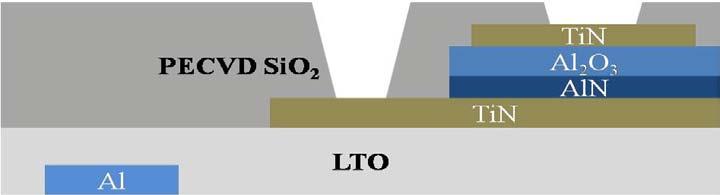
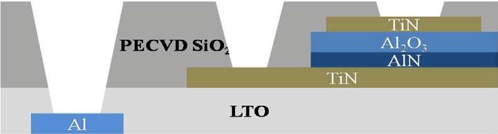
49 4.2. Integration of N-doped AlO x RRAM with CMOS Figure 4.2 illustrates the process flow for integration of N-AlO x RRAM on top of selection transistors. Figure 4.2 (a) starts with CMOS transistors already integrated in the substrate (not shown), connected with the Al layer shown. The Al layer is connected to the drain contact of a selection transistor, but the connections to source and gate contacts are not shown in Figure 4.2. We started with silicon oxide layer where LTO densification was performed at 400 C as shown in Figure 4.2 (a). On top of LTO layer, we deposited RRAM stacks consisting of 20 nm thick bottom TiN electrode, 4 nm thick AlN, 5 nm thick Al 2 O 3, and 20 nm thick top TiN electrode as shown in Figure 4.2 (b). The bottom electrode is composed of 5nm ALD TiN on top of 15 nm PVD TiN, whereas the top electrode is 15nm PVD TiN on top of 5nm ALD TiN. The ALD layers, TiN bottom electrode, AlN, Al 2 O 3, and TiN top electrode are deposited in-situ to prevent any oxidation or contamination along the interfaces. (a) (b) (c) 37
 (g)")

50 (d) (e) (f) (g) (h) 38
 and (e), respectively.")
51 (i) (j) Figure 4.2: Illustration of the process flow for integration of N-AlO x on top of selection transistors. In Figure 4.2 (c), RRAM area was defined by etching four layers. In next steps, bottom electrode for RRAM cells was patterned and was followed by top electrode patterning as shown in Figure (d) and (e), respectively. Fluorine gas etches TiN or SiO 2 layer, not Al 2 O 3 or AlN layer. Similarly, chlorine gas etches Al 2 O 3 or AlN layer chemically, but not TiN or SiO 2 layer. This makes selective etching feasible. Next, we deposited 200 nm plasma enhanced chemical vapor deposition (PECVD) oxide for the purpose of isolation as shown in Figure 4.2 (f). Here, the topology of PECVD oxide was oversimplified such that the surface of PECVD oxide layer is flat and smooth. In reality, the surface of the oxide layer is not flat, but this doesn t affect conclusion that will be discussed in this dissertation. In step (g) and (h), contact vias for top and bottom TiN electrode were made and were followed by making contact vias for source, drain, gate, and body of a selection transistor, respectively. Next, titanium barrier layer and aluminum interconnection 39

 illustrates top view of fabricated 1T1R structure and how TiN bottom electrode is connected to")
 shows a cross section schematic of 1T1R structure. (a) (b) (c) Figure 4.")
52 layer were deposited and were patterned as shown in Figure 4.2 (i) and (j), respectively. For the last step, final annealing at 400 C for 15 minutes were performed. Figure 4.3 (a) shows a SEM cross-sectional view of RRAM stacks. Figure 4.3 (b) illustrates top view of fabricated 1T1R structure and how TiN bottom electrode is connected to the drain region of a NMOS selection transistor. Figure 4.3 (c) shows a cross section schematic of 1T1R structure. (a) (b) (c) Figure 4.3: (a) Cross-sectional view of RRAM stacks, (b) top view of 1T1R structure, and (c) cross-sectional schematic of 1T1R structure. 40

53 Figure 4.4: Cross-sectional view of RRAM stacks that were deposited in a via region. In this experiment, we also considered topography of RRAM stacks. The RRAM stacks were not deposited in a via region directly. If RRAM stacks were deposited in the via region as shown in Figure 4.4, films that were deposited on the sidewalls of the via tend to be thinned, and therefore most current will flow across the thinned RRAM stacks on the sidewalls. This will affect the reliability of RRAM stacks. For this reason, we prefer planar structure Description of 1Transistor 1RRAM structure Figure 4.5 (a) shows a snap shot of the test chip. The 1T1R cell area is enlarged in Figure 4.5 (b). In Figure 4.5, m1 to m4 correspond to column of transistors with different width or length as summarized in Table 4.1. In each column, 13 RRAM cells with different sizes are located and these are summarized in Table 4.2. In these RRAM sets, we conservatively chose RRAM cell size of 1um X 1um for detailed characterization. 41
 Test chip")

54 (a) (b) Figure 4.5: (a) Test chip snapshot and (b) an enlarged view of 1T1R RRAM area. 42
55 RRAM 10 um 5 um 1 um 0.9 um 0.8 um 0.7 um 0.6 um cells size X 10 um X 5 um X 1 um X 0.9 um X 0.8 um X 0.7 um X 0.6 um RRAM 0.5 um 1.5 um 1.4 um 1.3 um 1.2 um 1.1 um cells size X 0.5 um X 1.5 um X 1.4 um X 1.3 um X 1.2 um X 1.1 um Table 4.2: RRAM cells of different sizes. The numbering corresponds to those shown in Figure 4.5 (b). 43
56 Chapter 5: Electrical switching characteristics of N-doped AlO X RRAM grown by ALD In this chapter, switching characteristics of 1T1R N-AlO x RRAM cells will be discussed in details. Before we discuss characteristics, measurement set-up for characterization of N-AlO x will be introduced in the following section Measurement setup for 1T1R structure Set Reset V Applied Gnd V G V G Gnd V Applied (a) (b) Figure 5.1: Illustration of measurement set-up for (a) set and (b) reset switching. 44
57 Figure 5.1 illustrates the configurations for measuring the 1T1R structure. As shown in Figure 5.1, V G indicates a gate bias and RRAM cells are connected to the drain contact directly. With this configuration, the parasitic capacitance is minimized, and instantaneous switching prevents over-programming [35]. This explains why 1T1R structures show reliable and uniform switching characteristics. When we set a memory cell, a small bias is applied to the gate so that the selection transistor operates in the sub-threshold region and as a result controls current level of nano-ampere. This is because our N-AlO x RRAM cells can be programmed with an applied current below micro-ampere range I-V switching characteristics 600.0p Set 300.0p Current(A) p p Reset Voltage(V) Figure 5.2: I-V switching characteristics of ALD N-AlO x RRAM. 45
58 800.0p 600.0p 1st set cycle 2nd set cycle Set current(a) 400.0p 200.0p Voltage(V) Figure 5.3: Illustration of set switching behaviors showing no forming process. I-V switching characteristics of N-AlO x RRAM are shown in Figure 5.2. Arrows indicate switching sequence of N-AlO x RRAM cells. Memory cells start in the high resistance state of about 1 GΩ. At about voltage of 2.4 V memory cells will be set from the low resistance state to the high resistance state with an applied current as low as 600 pa. A negative voltage of 1.8 V will be applied to reset memory cells back to the high resistance state. The current that is required to reset memory cells can be as low as 800 pa. The resulting on-off ratio, which is defined as ratio off-resistance to on-resistance, is about 20, which is insufficient for multi-bit storage. However, this does illustrate the potential of this technology for low power application. Figure 5.3 compares the 1st set cycle with the subsequent set cycle. Set voltage is defined as the point where current flowing across memory cells abruptly jumps into high level of current, and no significant difference in the set voltage between the 1st and the 2nd set cycle is detected. This indicates the N-AlO x RRAM is a forming free device. We believe that a moderate amount of traps is required to facilitate resistive switching behavior. If less traps exist in the resistive 46
59 dielectric films, a high voltage is needed to be applied across the film to create traps that are necessary for RRAM operations, which explains a forming process. On the other hand, many traps in resistive dielectric films may result in forming free switching behavior but at the same time make the films leaky which is not desirable for low power application. In addition, it is difficult to precisely control the amount of traps caused by oxygen vacancies due to strong preference of aluminum to bond with oxygen. However, we can obtain a moderate amount of traps by incorporating nitrogen into aluminum oxide because chemical reaction of nitrogen to aluminum is not as strong as that of oxygen to aluminum and the incorporation of nitrogen into aluminum oxide is limited. We believe that the incorporation of nitrogen results in a uniform density of traps that are necessary for RRAM operations and removes the forming process n 15nA-V G =300mV Current(A) 120.0n 90.0n 60.0n 30.0n 35nA-V G =310mV 80nA-V G =320mV 120nA-V G =330mV Voltage(V) (a) 47
60 Current(A) 150.0n 120.0n 90.0n 60.0n 30.0n 15nA-V G =300mV 35nA-V G =310mV 80nA-V G =320mV 120nA-V G =330mV Voltage(V) (b) Figure 5.4: Set switching behavior as a function of the gate bias of selection transistors for (a) ALD N-AlO x 1T1R structure and (b) PVD N-AlO x 1T1R structure, respectively. Since we have a 1T1R configuration, we can control set current by adjusting the gate bias of the selection transistor. Figure 5.4 shows set switching behavior of ALD and PVD N-AlO x 1T1R structure as a function of the gate bias of the selection transistor. The switching conditions such as set compliance current and the gate bias are inserted. For both ALD and PVD 1T1R structure, a few hundreds mv for the gate bias indicates the selection transistor operates in the sub-threshold region, and drain current of the selection transistor increases with the gate bias. Figure 5.4 also shows that the set voltage of ALD N-AlO x 1T1R is less sensitive to the gate bias. 48
61 5.3. Programming voltage distribution PVD ALD Cum. Probability Reset Voltage(V) (a) 100 PVD 80 ALD Cum. probability Set voltage(v) Figure 5.5: Distributions of (a) set and (b) reset voltages of N-AlO x. The set and reset current are limited to 300 na and 1 ua, respectively. (b) 49
62 Distributions of set and reset voltages for ALD and PVD N-AlO x 1T1R structure are plotted in Figure 5.5. This type of statistical study such as distributions of switching parameters will be a useful guideline when array of RRAM cells are implemented in circuit systems. If these parameters are distributed broadly, circuits must be designed to guarantee reliable operation, usually with a sacrifice in circuit performance. Therefore, a tight distribution of switching parameters is highly desirable. As shown in Figure 5.5, ALD N-AlO x RRAM cells show a tighter distribution of set and reset voltages than that of PVD N-AlO x RRAM cells. We believe that the tight distribution is due to the improved uniformity of films deposited by ALD. 50
63 5.4. Set/reset current versus on resistance 1µ PVD ALD Set Current(A) 100n 10n 100k 1M 10M 100M 1G On-Resistance(Ω) (a) Reset Current(A) 10µ 1µ 100n 10n PVD ALD 100k 1M 10M 100M 1G On-Resistance(Ω) (b) Figure 5.6: (a) Set current versus on-resistance and (b) reset current versus on-resistance. 51
64 In section 5.2, I-V characteristics of forming free N-AlO x RRAM were shown, and the resulting on/off ratio was not sufficient for multi-bit storage. A higher set current should be used to accommodate for multi-bit storage. With 1T1R configuration, we can control the set current by adjusting the gate bias of the selection transistor. Figure 5.6 illustrates the relationship between set/reset current and on-resistance. In this figure, the on-resistance was defined as the ratio of voltage and current at an applied voltage of 0.3 V. If a higher set current is used, the resulting onresistance will be lower. Conversely, a lower set current will result in higher on-resistance as shown in Figure 5.6 (a). As expected, the selection transistor successfully limits the set current and therefore on-resistance is precisely controlled by the gate bias of the selection transistor. In Figure 5.6 (b), for lower on-resistance a higher reset current is required, and higher on-resistance requires a lower reset current. In the case of no selection transistors or diodes, the reset current is higher than the set current. However, the electrical damage that may occur during the set process can be minimized by using the selection transistor, and therefore the reset currents can be comparable to the set currents [21]. Overall, the selection transistor controls the set current and thereby on-resistance, and finally the resulting on-resistance determines the subsequent reset current. The strong relationship between the set or reset current and on-resistance is observed for both ALD and PVD N-AlO x RRAM. Based on the relationship, we can control on-off resistance ratio to accommodate for multi-bit storage; for an on-off resistance ratio of 10 3 with 1 MΩ onresistance, the set current less than 1 ua is required, and the reset current below 10 ua is required. These levels of currents for ALD N-AlO x are comparable with those for PVD N-AlO x and still very low compared with other published RRAM results[11,24]. In addition, ALD N-AlO x RRAM cells show a tight distribution, which is consistent with the tight distributions of set and reset voltages as illustrated in Figure 5.5. We believe that the uniformity of films affects switching characteristics and this is why ALD N-AlO x RRAM cells show tighter distributions and better performance than PVD N-AlO x RRAM cells. 52
65 5.5. Linear and non-linear I-V characteristics of HRS and various LRS LRS(1.2kΩ) LRS(1.2MΩ) LRS(29.2MΩ) HRS(0.91GΩ) ln(i) Voltage( V) Figure 5.7: Plot of natural log of current versus square root of voltage for HRS and various LRS. As illustrated in Section 5.2, RRAM cells can be set to various low resistance states by controlling the gate bias of the selection transistor. Natural log of current versus square root of voltage for various low resistance states and the high resistance state are plotted in Figure 5.7. The on-resistance was determined by the ratio of the applied voltage of 0.3 V to an applied current. The low voltage applied across RRAM cells during resistance measurement prevents any programming. For on-resistance of below 100 kω, the RRAM shows Ohmic linear conduction behavior. When the RRAM is set to above 100 kω, the on-state conduction is no longer linear, but exhibits rectifying behavior instead. In addition, the off-conduction is not Ohmic. This nonlinear conduction behavior can be shown in natural log of current versus square root of voltage plot. This relationship implies that the carrier flow in the resistive dielectric films is limited by a 53
66 potential barrier. There are two well-known conduction models, Frankel-Poole emission model and Schottky emission model, that describe this type of behavior. We believe that Frenkel-Poole conduction behavior is associated with the AlN traps and oxygen-vacancy traps in the AlO x where these traps are involved in the conduction. Larger set currents would increase the density of traps, and as a result the increased traps lead to the lowering of the potential barrier[36]. This explains that the on-resistance decreases when the set current is increased. If the set current is further increased, the density of traps can reach the point where the current conduction behavior becomes Ohmic. 1G Resistance(Ω) 100M 10M 1M 100k 10k HRS HRS(290MΩ) LRS(1.6MΩ) (1.6M) LRS LRS(510kΩ) LRS LRS(1.5kΩ) 1k Temperature( C) Figure 5.8: Dependency on temperature of HRS and various LRS. To understand switching characteristics, we also studied temperature dependence of the non-ohmic conduction behavior. The RRAM cells were programmed in the high resistance state and various low resistance states at room temperature. They were heated from 30 C to 90 C where their resistances were measured at each temperature. Figure 5.8 shows the dependency of those resistance states on temperature. For LRS below 100 kω, the resistance increases with 54
67 temperature. This implies that the conduction is Ohmic conduction, which is consistent with the result discussed in the previous section. On the other hand, for HRS and LRS above 100 kω, the resistance decreases with temperature. This is consistent with non-linear conduction behavior. As temperature increases, carriers in resistive dielectric films gain energy, and therefore more carriers can surmount the potential barrier and contribute to the conduction. This is typical of Frenkel-Poole conduction behavior at high temperature. 55
68 5.6. Conduction mechanism in ALD N-AlO x RRAM In the previous section, two different conduction behaviors, metallic and rectifying conduction, of ALD N-AlO x RRAM were observed. In this section, we will focus on the nonlinear rectifying conduction behavior. To understand non-linear conduction behavior, we applied two common models, Frenkel-Poole emission model as described by equation 5.1, and Schottky emission model as described by equation 5.2, to our experimental data [37]. An almost linear dependency between the natural log of current and the square root of voltage exists in both models. J AT 2 exp ( q(φ qe/(4πε ε ) B r 0 ) k B T J Eexp ( q(φ qe/(πε ε ) T r 0 ) k B T (5.1) (5.2) In the equations, A is the effective Richardson constant, T is the absolute temperature, k B is the Boltzmann constant, ɛ 0 is the permittivity of free space, ɛ r is relative permittivity of the resistive dielectric films. E is the intensity of electric field and is given by the ratio of the applied voltage to the dielectric thickness. ϕ B and ϕ T are the energy barrier height in the respective model. In this experiment, we measured I-V characteristics of various resistance states. Under different temperature from 40 C to 55 C, each I-V curve is fitted to a linear dependence between the natural log of current and the square root of voltage as shown in Figure 5.9 [21]. These results show that current increases as temperature is increased and there is a linear dependence between the natural log of current and the square root of voltage at each temperature. The current conduction mechanism is the same at these ranges. 56
69 ln(i) C 40 C Voltage 1/2 ( V) Increase by 5 C (a) ln(i) Voltage 1/2 ( V) (b) 55 C Increase by 5 C 40 C Figure 5.9: I-V relationship of (a) HRS and (b) LRS at various temperatures. 57
70 -16 ln(i) LRS HRS /kT Figure 5.10: Temperature dependence of HRS and LRS. The next step is to verify the dependency of the natural log of current on temperature. Figure 5.10 illustrates the natural log of current is proportional to kt. The results obtained as depicted in Figure 5.9 and Figure 5.10 support that the current conduction in our ALD N-AlO x RRAM is either Frenkel-Poole emission or Schottky emission. In the last step, we calculated the energy barriers using the non-linear I-V curve for both emission models to determine the best fit to our experimental results. Figure 5.11 illustrates the fitting results to the Frenkel-Poole emission model. If we extrapolate to the Y axis in this plot, the intersection is the intrinsic trap barrier height at the zero electric field [21]. A trap energy barrier height of about 0.53 ev is calculated for the high resistance state (0.95 GΩ), and the energy barrier height of about 0.22 ev and 0.15 ev are obtained for low resistance states (18.1 MΩ and 5.1 MΩ, respectively). We also applied the Schottky emission model to experimental data as shown in Figure The fitting results for the model led to unreasonably low energy barrier height (a few kt) [37]. This suggests that the Frenkel-Poole emission model is the best description of conduction in ALD N-AlO x RRAM. 58
71 Enery barrier(ev) eV 0.525eV HRS(0.95GΩ) LRS(18.1MΩ) LRS(5.1MΩ) 0.145eV Voltage 1/2 (V 1/2 ) Figure 5.11: Illustration of curve-fitting for the Frenkel-Poole emission model. Energy barrier (ev) eV 0.07eV HRS (0.95 GΩ) LRS (5.1 MΩ) Voltage 1/2 (V 1/2 ) Figure 5.12: Illustration of curve-fitting for the Schottky emission model. 59
 after an annealing process and (b) after a set process.")
, the discrete energy level that is located 0.")
72 (a) (b) Figure 5.13: Energy band diagram of (a) after an annealing process and (b) after a set process. Figure 5.13 shows a speculative band model for ALD N-doped AlO x RRAM. As shown in Figure 5.13 (a), the discrete energy level that is located 0.53 ev below conduction band is created after the annealing process. This discrete energy level is caused by AlN x traps that are 60
Resistive switching of CeO x /SiO 2 stacked film based on anodic oxidation and breakdown
 Feb. 19 th, 2015 WIMNACT-45 Resistive switching of /SiO 2 stacked film based on anodic oxidation and breakdown K. Kakushima Tokyo Institute of Technology 1 Introduction to resistive RAM (RRAM) Reset OFF
Redox-Active Molecular Flash Memory for On-Chip Memory
 Redox-Active Molecular Flash Memory for On-Chip Memory By Hao Zhu Electrical and Computer Engineering George Mason University, Fairfax, VA 2013.10.24 Outline Introduction Molecule attachment method & characterizations
Supplementary Information
 Monitoring Oxygen Movement by Raman Spectroscopy of Resistive Random Access Memory with a Graphene-Inserted Electrode Supplementary Information He Tian, 1,2 Hong-Yu Chen, 3 Bin Gao, 3,4 Shimeng Yu, 3 Jiale
Lecture Day 2 Deposition
 Deposition Lecture Day 2 Deposition PVD - Physical Vapor Deposition E-beam Evaporation Thermal Evaporation (wire feed vs boat) Sputtering CVD - Chemical Vapor Deposition PECVD LPCVD MVD ALD MBE Plating
CHAPTER 4: Oxidation. Chapter 4 1. Oxidation of silicon is an important process in VLSI. The typical roles of SiO 2 are:
 Chapter 4 1 CHAPTER 4: Oxidation Oxidation of silicon is an important process in VLSI. The typical roles of SiO 2 are: 1. mask against implant or diffusion of dopant into silicon 2. surface passivation
Fairchild Semiconductor Application Note June 1983 Revised March 2003
 Fairchild Semiconductor Application Note June 1983 Revised March 2003 High-Speed CMOS (MM74HC) Processing The MM74HC logic family achieves its high speed by utilizing microcmos Technology. This is a 3.5
Resistive Transition Metal Oxide Memory
 Resistive Transition Metal Oxide Memory Senior Project Microelectronic Engineering Wilkie Olin-Ammentorp, Microelectronic Engineering Advisor: Santosh Kurinec 5/11/2015 Introduction to Memory Many different
A Novel Low Temperature Self-Aligned Field Induced Drain Polycrystalline Silicon Thin Film Transistor by Using Selective Side-Etching Process
 Chapter 3 A Novel Low Temperature Self-Aligned Field Induced Drain Polycrystalline Silicon Thin Film Transistor by Using Selective Side-Etching Process 3.1 Introduction Low-temperature poly-si (LTPS) TFTs
ELEC 7364 Lecture Notes Summer Si Oxidation. by STELLA W. PANG. from The University of Michigan, Ann Arbor, MI, USA
 ELEC 7364 Lecture Notes Summer 2008 Si Oxidation by STELLA W. PANG from The University of Michigan, Ann Arbor, MI, USA Visiting Professor at The University of Hong Kong The University of Michigan Visiting
EE 143 FINAL EXAM NAME C. Nguyen May 10, Signature:
 INSTRUCTIONS Read all of the instructions and all of the questions before beginning the exam. There are 5 problems on this Final Exam, totaling 143 points. The tentative credit for each part is given to
2-1 Introduction The demand for high-density, low-cost, low-power consumption,
 Chapter 2 Hafnium Silicate (HfSi x O y ) Nanocrystal SONOS-Type Flash Memory Fabricated by Sol-Gel Spin Coating Method Using HfCl 4 and SiCl 4 as Precursors 2-1 Introduction The demand for high-density,
Thermal Evaporation. Theory
 Thermal Evaporation Theory 1. Introduction Procedures for depositing films are a very important set of processes since all of the layers above the surface of the wafer must be deposited. We can classify
Chapter 3. In this chapter, we use sol-gel method to combine three high-k precursors, i.e. HfCl 4, ZrCl 4 and SiCl 4 together to form hafnium silicate
 Chapter 3 Sol-Gel-Derived Zirconium Silicate (ZrSi x O y ) and Hafnium Silicate (HfSi x O y ) Co-existed Nanocrystal SONOS Memory 3-1 Introduction In the previous chapter, we fabricate the sol-gel-derived
X-Ray Reflectivity Study of Hafnium Silicate Thin Films Prepared by Thermal Chemical Vapor Deposition
 X-Ray Reflectivity Study of Hafnium Silicate Thin Films Prepared by Thermal Chemical Vapor Deposition Hideyuki YAMAZAKI, Advanced LSI Technology Laboratory, Toshiba Corporation hideyuki.yamazaki@toshiba.co.jp
Oxide Growth. 1. Introduction
 Oxide Growth 1. Introduction Development of high-quality silicon dioxide (SiO2) has helped to establish the dominance of silicon in the production of commercial integrated circuits. Among all the various
Non-charge Storage Resistive Memory: How it works
 Accelerating the next technology revolution Non-charge Storage Resistive Memory: How it works Gennadi Bersuker Copyright 2009 SEMATECH, Inc. SEMATECH, and the SEMATECH logo are registered servicemarks
Radiation Tolerant Isolation Technology
 Radiation Tolerant Isolation Technology Background The following contains a brief description of isolation technologies used for radiation hardened integrated circuits. The technologies mentioned are junction
Silicon Epitaxial CVD Want to create very sharp PN boundary grow one type layer on other in single crystal form High dopant layers on low dopant
 Silicon Epitaxial CVD Want to create very sharp PN boundary grow one type layer on other in single crystal form High dopant layers on low dopant substrate Creates latch up protection for CMOS Buried Epi
Lecture 0: Introduction
 Lecture 0: Introduction Introduction Integrated circuits: many transistors on one chip. Very Large Scale Integration (VLSI): bucketloads! Complementary Metal Oxide Semiconductor Fast, cheap, low power
In-situ Monitoring of Atomic Layer Deposition Processes
 Faculty of Electrical and Computer Engineering - Institute of Semiconductors and Microsystems NanoZEIT seminar @ SEMICON 2011 Deposition Processes M. Knaut*, M. Junige, M. Geidel, M. Albert, and J. W.
Science of Advanced Materials
 Manuscript Template Science of Advanced Materials (www.aspbs.com/sam) Polarity Reversion of the Operation Mode of HfO2-Based Resistive Random Access Memory Devices by Inserting Hf Metal Layer Ching-Shiang
Plasma-Enhanced Chemical Vapor Deposition
 Plasma-Enhanced Chemical Vapor Deposition Steven Glenn July 8, 2009 Thin Films Lab 4 ABSTRACT The objective of this lab was to explore lab and the Applied Materials P5000 from a different point of view.
Fabrication of Ru/Bi 4-x La x Ti 3 O 12 /Ru Ferroelectric Capacitor Structure Using a Ru Film Deposited by Metalorganic Chemical Vapor Deposition
 Mat. Res. Soc. Symp. Proc. Vol. 784 2004 Materials Research Society C7.7.1 Fabrication of Ru/Bi 4-x La x Ti 3 O 12 /Ru Ferroelectric Capacitor Structure Using a Ru Film Deposited by Metalorganic Chemical
Passivation of InAs and GaSb with novel high dielectrics
 Passivation of InAs and GaSb with novel high dielectrics Professor Minghwei HONG Department of Materials Science and Engineering, National Tsing Hua University 101, Section 2, Kuang-Fu Rd., Hsinchu, Taiwan,
Instructor: Dr. M. Razaghi. Silicon Oxidation
 SILICON OXIDATION Silicon Oxidation Many different kinds of thin films are used to fabricate discrete devices and integrated circuits. Including: Thermal oxides Dielectric layers Polycrystalline silicon
PROCESS FLOW AN INSIGHT INTO CMOS FABRICATION PROCESS
 Contents: VI Sem ECE 06EC63: Analog and Mixed Mode VLSI Design PROCESS FLOW AN INSIGHT INTO CMOS FABRICATION PROCESS 1. Introduction 2. CMOS Fabrication 3. Simplified View of Fabrication Process 3.1 Alternative
DEPOSITION AND CHARACTERISTICS OF TANTALUM NITRIDE FILMS BY PLASMA ASSISTED ATOMIC LAYER DEPOSITION AS CU DIFFUSION BARRIER
 Mat. Res. Soc. Symp. Proc. Vol. 766 2003 Materials Research Society E3.22.1 DEPOSITION AND CHARACTERISTICS OF TANTALUM NITRIDE FILMS BY PLASMA ASSISTED ATOMIC LAYER DEPOSITION AS CU DIFFUSION BARRIER Kyoung-Il
Silicon Epitaxial CVD Want to create very sharp PN boundary grow one type layer on other in single crystal form High dopant layers on low dopant
 Silicon Epitaxial CVD Want to create very sharp PN boundary grow one type layer on other in single crystal form High dopant layers on low dopant substrate Creates latch up protection for CMOS Buried Epi
VLSI. Lecture 1. Jaeyong Chung System-on-Chips (SoC) Laboratory Incheon National University. Based on slides of David Money Harris
 Laboratory Incheon National University. Based on slides of David Money Harris") VLSI Lecture 1 Jaeyong Chung System-on-Chips (SoC) Laboratory Incheon National University Based on slides of David Money Harris Goals of This Course Learn the principles of VLSI design Learn to design
VLSI Lecture 1 Jaeyong Chung System-on-Chips (SoC) Laboratory Incheon National University Based on slides of David Money Harris Goals of This Course Learn the principles of VLSI design Learn to design
Is Now Part of To learn more about ON Semiconductor, please visit our website at
 Is Now Part of To learn more about ON Semiconductor, please visit our website at www.onsemi.com ON Semiconductor and the ON Semiconductor logo are trademarks of Semiconductor Components Industries, LLC
Advanced Science, Engineering and Medicine
 Manuscript Template Advanced Science, Engineering and Medicine (www.aspbs.com/asem) Polarity Reversion of the Operation Mode of HfO2-Based Resistive Random Access Memory Devices by Inserting Hf Metal Layer
Impact of Filament Evolution on Reliability Issues of Oxide Electrolyte Based Conductive Bridge Random Access Memory
 Impact of Filament Evolution on Reliability Issues of Oxide Electrolyte Based Conductive Bridge Random Access Memory Hangbing Lv, Xiaoxin Xu, Hongtao Liu, Qing Luo, Qi Liu, Shibing Long, Ming Liu* Institute
Silver Diffusion Bonding and Layer Transfer of Lithium Niobate to Silicon
 Chapter 5 Silver Diffusion Bonding and Layer Transfer of Lithium Niobate to Silicon 5.1 Introduction In this chapter, we discuss a method of metallic bonding between two deposited silver layers. A diffusion
Technology. Semiconductor Manufacturing. Hong Xiao INTRODUCTION TO SECOND EDITION SPIE PRESS
 INTRODUCTION TO Semiconductor Manufacturing Technology SECOND EDITION Hong Xiao TECHNISCHE INFORMATIONSBiBUOTHEK UNIVERSITATSBIBLIOTHEK HANNOVER SPIE PRESS Bellingham,Washington USA Contents Preface to
VLSI INTRODUCTION P.VIDYA SAGAR ( ASSOCIATE PROFESSOR) Department of Electronics and Communication Engineering, VBIT
 Department of Electronics and Communication Engineering, VBIT") VLSI INTRODUCTION P.VIDYA SAGAR ( ASSOCIATE PROFESSOR) contents UNIT I INTRODUCTION: Introduction to IC Technology MOS, PMOS, NMOS, CMOS & BiCMOS technologies. BASIC ELECTRICAL PROPERTIES : Basic Electrical
VLSI INTRODUCTION P.VIDYA SAGAR ( ASSOCIATE PROFESSOR) contents UNIT I INTRODUCTION: Introduction to IC Technology MOS, PMOS, NMOS, CMOS & BiCMOS technologies. BASIC ELECTRICAL PROPERTIES : Basic Electrical
Department of Electrical Engineering. Jungli, Taiwan
 Chapter 3 Fabrication of CMOS Integrated Circuits Jin-Fu Li Department of Electrical Engineering National Central University Jungli, Taiwan Background Outline The CMOS Process Flow Design Rules Latchup
Hei Wong.
 Defects and Disorders in Hafnium Oxide and at Hafnium Oxide/Silicon Interface Hei Wong City University of Hong Kong Email: heiwong@ieee.org Tokyo MQ2012 1 Outline 1. Introduction, disorders and defects
IC/MEMS Fabrication - Outline. Fabrication
 IC/MEMS Fabrication - Outline Fabrication overview Materials Wafer fabrication The Cycle: Deposition Lithography Etching Fabrication IC Fabrication Deposition Spin Casting PVD physical vapor deposition
ECSE-6300 IC Fabrication Laboratory Lecture 4: Dielectrics and Poly-Si Deposition. Lecture Outline
 ECSE-6300 IC Fabrication Laboratory Lecture 4: Dielectrics and Poly-Si Deposition Prof. Rensselaer Polytechnic Institute Troy, NY 12180 Office: CII-6229 Tel.: (518) 276-2909 e-mails: luj@rpi.edu http://www.ecse.rpi.edu/courses/s18/ecse
Review of CMOS Processing Technology
 - Scaling and Integration Moore s Law Unit processes Thin Film Deposition Etching Ion Implantation Photolithography Chemical Mechanical Polishing 1. Thin Film Deposition Layer of materials ranging from
EE 143 CMOS Process Flow
 EE 143 CMOS rocess Flow CT 84 D D G Sub G Sub S S G D S G D S + + + + - MOS Substrate Well - MOS Substrate EE 143 CMOS rocess Flow CT 85 hotoresist Si 3 4 SiO 2 Substrate selection: moderately high resistivity,
SUPPLEMENTARY INFORMATIONS
 SUPPLEMENTARY INFORMATIONS Dynamic Evolution of Conducting Nanofilament in Resistive Switching Memories Jui-Yuan Chen, Cheng-Lun Hsin,,, Chun-Wei Huang, Chung-Hua Chiu, Yu-Ting Huang, Su-Jien Lin, Wen-Wei
A study on resistive-switching behavior of CeO 2 metal-insulator-metal structures for resistance random access memory devices
 2011 Master thesis A study on resistive-switching behavior of CeO 2 metal-insulator-metal structures for resistance random access memory devices Supervisor Professor Nobuyuki Sugii Department of Electronics
Doping and Oxidation
 Technische Universität Graz Institute of Solid State Physics Doping and Oxidation Franssila: Chapters 13,14, 15 Peter Hadley Technische Universität Graz Institute of Solid State Physics Doping Add donors
Czochralski Crystal Growth
 Czochralski Crystal Growth Crystal Pulling Crystal Ingots Shaping and Polishing 300 mm wafer 1 2 Advantage of larger diameter wafers Wafer area larger Chip area larger 3 4 Large-Diameter Wafer Handling
TANOS Charge-Trapping Flash Memory Structures
 TANOS Charge-Trapping Flash Memory Structures A Senior Design by Spencer Pringle 5/8/15 Table of Contents Motivation Why Charge-Trapping Flash (CTF)? Charge-Trapping vs. Floating Gate Electronically-Erasable
Make sure the exam paper has 9 pages total (including cover page)
") UNIVERSITY OF CALIFORNIA College of Engineering Department of Electrical Engineering and Computer Sciences Fall 2010 EE143 Midterm Exam #2 Family Name First name SID Signature Solution Make sure the exam
UNIVERSITY OF CALIFORNIA College of Engineering Department of Electrical Engineering and Computer Sciences Fall 2010 EE143 Midterm Exam #2 Family Name First name SID Signature Solution Make sure the exam
CMOS Technology. Flow varies with process types & company. Start with substrate selection. N-Well CMOS Twin-Well CMOS STI
 CMOS Technology Flow varies with process types & company N-Well CMOS Twin-Well CMOS STI Start with substrate selection Type: n or p Doping level, resistivity Orientation, 100, or 101, etc Other parameters
Effect of annealing temperature on the electrical properties of HfAlO thin films. Chun Lia, Zhiwei Heb*
 International Forum on Energy, Environment and Sustainable Development (IFEESD 2016) Effect of annealing temperature on the electrical properties of HfAlO thin films Chun Lia, Zhiwei Heb* Department of
Lecture 4. Oxidation (applies to Si and SiC only) Reading: Chapter 4
 Reading: Chapter 4") Lecture 4 Oxidation (applies to Si and SiC only) Reading: Chapter 4 Introduction discussion: Oxidation: Si (and SiC) Only The ability to grow a high quality thermal oxide has propelled Si into the forefront
Lecture 4 Oxidation (applies to Si and SiC only) Reading: Chapter 4 Introduction discussion: Oxidation: Si (and SiC) Only The ability to grow a high quality thermal oxide has propelled Si into the forefront
Growth and Doping of SiC-Thin Films on Low-Stress, Amorphous Si 3 N 4 /Si Substrates for Robust Microelectromechanical Systems Applications
 Journal of ELECTRONIC MATERIALS, Vol. 31, No. 5, 2002 Special Issue Paper Growth and Doping of SiC-Thin Films on Low-Stress, Amorphous Si 3 N 4 /Si Substrates for Robust Microelectromechanical Systems
ALD of Scandium Oxide from Tris(N,N -diisopropylacetamidinato)scandium and Water
scandium and Water") ALD of Scandium Oxide from Tris(N,N -diisopropylacetamidinato)scandium and Water Philippe P. de Rouffignac, Roy G. Gordon Dept. of Chemistry,, Cambridge, MA gordon@chemistry.harvard.edu (617) 495-4017
ALD of Scandium Oxide from Tris(N,N -diisopropylacetamidinato)scandium and Water Philippe P. de Rouffignac, Roy G. Gordon Dept. of Chemistry,, Cambridge, MA gordon@chemistry.harvard.edu (617) 495-4017
RADIATION HARDNESS OF MEMRISTIVE SYSTEMS
 RADIATION HARDNESS OF MEMRISTIVE SYSTEMS A. FANTINI ON BEHALF OF IMEC RRAM TEAM AND VU ISDE TEAM Workshop on Memristive systems for Space applications ESTEC - 30/04/2015 OUTLINE Introduction RRAM for space
Characterization of Interfacial Oxide Layers in Heterostructures of Hafnium Oxides Formed on NH 3 -nitrided Si(100)
") Characterization of Interfacial Oxide Layers in Heterostructures of Hafnium Oxides Formed on H 3 -nitrided Si() Hiroshi akagawa, Akio Ohta, Fumito Takeno, Satoru agamachi, Hideki Murakami Seiichiro Higashi
Characterization of Interfacial Oxide Layers in Heterostructures of Hafnium Oxides Formed on H 3 -nitrided Si() Hiroshi akagawa, Akio Ohta, Fumito Takeno, Satoru agamachi, Hideki Murakami Seiichiro Higashi
Atomic Layer Deposition of Novel High Dielectric Constant Materials
 Atomic Layer Deposition of Novel High Dielectric Constant Materials Adam Kueltzo # & Julie Lam * Thornton Fractional North High School # and Maine East High School * August 2, 2007 University of Illinois
Design, Fabrication, and Characterization of Nano-scale Cross-Point Hafnium Oxide-Based Resistive Random Access Memory
 Design, Fabrication, and Characterization of Nano-scale Cross-Point Hafnium Oxide-Based Resistive Random Access Memory A Thesis Presented to The Academic Faculty By Noah Ellis In Partial Fulfillment Of
Metallization deposition and etching. Material mainly taken from Campbell, UCCS
 Metallization deposition and etching Material mainly taken from Campbell, UCCS Application Metallization is back-end processing Metals used are aluminum and copper Mainly involves deposition and etching,
FABRICATION of MOSFETs
 FABRICATION of MOSFETs CMOS fabrication sequence -p-type silicon substrate wafer -creation of n-well regions for pmos transistors, -impurity implantation into the substrate. -thick oxide is grown in the
EE 5344 Introduction to MEMS. CHAPTER 3 Conventional Si Processing
 3. Conventional licon Processing Micromachining, Microfabrication. EE 5344 Introduction to MEMS CHAPTER 3 Conventional Processing Why silicon? Abundant, cheap, easy to process. licon planar Integrated
Microelectronics. Integrated circuits. Introduction to the IC technology M.Rencz 11 September, Expected decrease in line width
 Microelectronics Introduction to the IC technology M.Rencz 11 September, 2002 9/16/02 1/37 Integrated circuits Development is controlled by the roadmaps. Self-fulfilling predictions for the tendencies
Lecture 12. Physical Vapor Deposition: Evaporation and Sputtering Reading: Chapter 12. ECE Dr. Alan Doolittle
 Lecture 12 Physical Vapor Deposition: Evaporation and Sputtering Reading: Chapter 12 Evaporation and Sputtering (Metalization) Evaporation For all devices, there is a need to go from semiconductor to metal.
Influence of Underlayer on Crystallography and Roughness of Aluminum Nitride Thin Film Reactively Sputtered by Ion-Beam Kaufman Source
 Influence of Underlayer on Crystallography and Roughness of Aluminum Nitride Thin Film Reactively Sputtered by Ion-Beam Kaufman Source GABLECH Imrich 1,*, SVATOŠ Vojtěch 1,, PRÁŠEK Jan 1,, HUBÁLEK Jaromír
Highly Reliable Low Temperature Ultrathin Oxides Grown Using N 2 O Plasma
 Highly Reliable Low Temperature Ultrathin Oxides Grown Using N 2 O Plasma Jam-Wem Lee 1, Yiming Li 1,2, and S. M. Sze 1,3 1 Department of Nano Device Technology, National Nano Device Laboratories, Hsinchu,
EE 330 Lecture 9. IC Fabrication Technology Part 2
 EE 330 Lecture 9 IC Fabrication Technology Part 2 Quiz 8 A 2m silicon crystal is cut into wafers using a wire saw. If the wire diameter is 220um and the wafer thickness is 350um, how many wafers will this
Technology Drivers for Plasma Prior to Wire Bonding
 Technology Drivers for Plasma Prior to Wire Bonding James D. Getty Nordson MARCH Concord, CA, USA info@nordsonmarch.com Technology Drivers for Plasma Prior to Wire Bonding Page 1 ABSTRACT Advanced packaging
EFFECT OF CRYSTALORIENTATIONIN OXIDATION PROCESS OF VLSI FABRICATION
 International Journal of Research in Engineering, Technology and Science, Volume VII, Special Issue, Feb 2017 www.ijrets.com, editor@ijrets.com, ISSN 2454-1915 EFFECT OF CRYSTALORIENTATIONIN OXIDATION
Lecture 22: Integrated circuit fabrication
 Lecture 22: Integrated circuit fabrication Contents 1 Introduction 1 2 Layering 4 3 Patterning 7 4 Doping 8 4.1 Thermal diffusion......................... 10 4.2 Ion implantation.........................
CMOS VLSI Design. Introduction. All materials are from the textbook Weste and Harris, 3 rd Edition CMOS VLSI DESIGN. Introduction
 CMOS VLSI Design Introduction ll materials are from the textbook Weste and Harris, 3 rd Edition CMOS VLSI DESIGN Introduction Chapter previews the entire field, subsequent chapters elaborate on specific
Activities in Plasma Process Technology at SENTECH Instruments GmbH, Berlin. Dr. Frank Schmidt
 Activities in Plasma Process Technology at SENTECH Instruments GmbH, Berlin Dr. Frank Schmidt The Company Company Private company, founded 1990 80 employees ISO 9001 Location Science & Technology Park,
High Density Plasma Etching of IrRu Thin Films as a New Electrode for FeRAM
 Integrated Ferroelectrics, 84: 169 177, 2006 Copyright Taylor & Francis Group, LLC ISSN 1058-4587 print / 1607-8489 online DOI: 10.1080/10584580601085750 High Density Plasma Etching of IrRu Thin Films
VLSI Technology Dr. Nandita Dasgupta Department of Electrical Engineering Indian Institute of Technology, Madras
 VLSI Technology Dr. Nandita Dasgupta Department of Electrical Engineering Indian Institute of Technology, Madras Lecture - 36 MOSFET I Metal gate vs self-aligned poly gate So far, we have discussed about
Thin Films: Sputtering Systems (Jaeger Ch 6 & Ruska Ch 7,) Can deposit any material on any substrate (in principal) Start with pumping down to high
 Can deposit any material on any substrate (in principal) Start with pumping down to high") Thin Films: Sputtering Systems (Jaeger Ch 6 & Ruska Ch 7,) Can deposit any material on any substrate (in principal) Start with pumping down to high vacuum ~10-7 torr Removes residual gases eg oxygen from
Thin Films: Sputtering Systems (Jaeger Ch 6 & Ruska Ch 7,) Can deposit any material on any substrate (in principal) Start with pumping down to high vacuum ~10-7 torr Removes residual gases eg oxygen from
ARTICLE IN PRESS. Materials Science in Semiconductor Processing
 Materials Science in Semiconductor Processing ] (]]]]) ]]] ]]] Contents lists available at ScienceDirect Materials Science in Semiconductor Processing journal homepage: www.elsevier.com/locate/mssp High-dielectric
CMOS FABRICATION. n WELL PROCESS
 CMOS FABRICATION n WELL PROCESS Step 1: Si Substrate Start with p- type substrate p substrate Step 2: Oxidation Exposing to high-purity oxygen and hydrogen at approx. 1000 o C in oxidation furnace SiO
HOMEWORK 4 and 5. March 15, Homework is due on Monday March 30, 2009 in Class. Answer the following questions from the Course Textbook:
 HOMEWORK 4 and 5 March 15, 2009 Homework is due on Monday March 30, 2009 in Class. Chapter 7 Answer the following questions from the Course Textbook: 7.2, 7.3, 7.4, 7.5, 7.6*, 7.7, 7.9*, 7.10*, 7.16, 7.17*,
Low Power VLSI Circuits and Systems Prof. Ajit Pal Department of Computer Science and Engineering Indian Institute of Technology, Kharagpur
 Low Power VLSI Circuits and Systems Prof. Ajit Pal Department of Computer Science and Engineering Indian Institute of Technology, Kharagpur Lecture No. # 02 MOS Transistors - I Hello and welcome to today
Atomic Layer Deposition (ALD)
") Atomic Layer Deposition (ALD) ALD provides Uniform, controlled, conformal deposition of oxide, nitride, and metal thin films on a nanometer scale. ALD is a self limiting thin film deposition technique
Atomic Layer Deposition (ALD) ALD provides Uniform, controlled, conformal deposition of oxide, nitride, and metal thin films on a nanometer scale. ALD is a self limiting thin film deposition technique
Amorphous and Polycrystalline Thin-Film Transistors
 Part I Amorphous and Polycrystalline Thin-Film Transistors HYBRID AMORPHOUS AND POLYCRYSTALLINE SILICON DEVICES FOR LARGE-AREA ELECTRONICS P. Mei, J. B. Boyce, D. K. Fork, G. Anderson, J. Ho, J. Lu, Xerox
MARORA A Plasma Selective-oxidation Apparatus for Metal-gate Devices
 Hitachi Review Vol. 57 (2008), No. 3 127 MARORA A Plasma Selective-oxidation Apparatus for Metal-gate Devices Tadashi Terasaki Masayuki Tomita Katsuhiko Yamamoto Unryu Ogawa, Dr. Eng. Yoshiki Yonamoto,
VLSI Technology. By: Ajay Kumar Gautam
 By: Ajay Kumar Gautam Introduction to VLSI Technology, Crystal Growth, Oxidation, Epitaxial Process, Diffusion Process, Ion Implantation, Lithography, Etching, Metallization, VLSI Process Integration,
ELEC 3908, Physical Electronics, Lecture 4. Basic Integrated Circuit Processing
 ELEC 3908, Physical Electronics, Lecture 4 Basic Integrated Circuit Processing Lecture Outline Details of the physical structure of devices will be very important in developing models for electrical behavior
200mm Next Generation MEMS Technology update. Florent Ducrot
 200mm Next Generation MEMS Technology update Florent Ducrot The Most Exciting Industries on Earth Semiconductor Display Solar 20,000,000x reduction in COST PER TRANSISTOR in 30 years 1 20x reduction in
Semiconductor Device Fabrication
 5 May 2003 Review Homework 6 Semiconductor Device Fabrication William Shockley, 1945 The network before the internet Bell Labs established a group to develop a semiconductor replacement for the vacuum
3D Vertical RRAM. Henry (Hong-Yu) Chen, H.-S. Philip Wong Stanford University, CA, USA Collaborator: Peking University, China
 Chen, H.-S. Philip Wong Stanford University, CA, USA Collaborator: Peking University, China") 3D Vertical RRAM Henry (Hong-Yu) Chen, H.-S. Philip Wong hongyuc@stanford.edu Stanford University, CA, USA Collaborator: Peking University, China Santa Clara, CA 1 What is RRAM? 0 : High Resistance State
3D Vertical RRAM Henry (Hong-Yu) Chen, H.-S. Philip Wong hongyuc@stanford.edu Stanford University, CA, USA Collaborator: Peking University, China Santa Clara, CA 1 What is RRAM? 0 : High Resistance State
Complementary Metal Oxide Semiconductor (CMOS)
") Technische Universität Graz Institute of Solid State Physics Complementary Metal Oxide Semiconductor (CMOS) Franssila: Chapters 26,28 Technische Universität Graz Institute of Solid State Physics Complementary
Technische Universität Graz Institute of Solid State Physics Complementary Metal Oxide Semiconductor (CMOS) Franssila: Chapters 26,28 Technische Universität Graz Institute of Solid State Physics Complementary
SiC high voltage device development
 SiC high voltage device development 2006. 11. 30 KERI Power Semiconductor Group outline 1. Device design & simulation for power devices 2. SiC power diode process development Ion implantation & activation
AMORPHOUS SILICON DIOXIDE LAYER FOR HIGH EFFICIENCY CRYSTALLINE SOLAR CELLS
 International Journal of Nanotechnology and Application (IJNA) ISSN(P): 2277-4777; ISSN(E): 2278-9391 Vol. 6, Issue 5, Dec 2016, 1-6 TJPRC Pvt. Ltd. AMORPHOUS SILICON DIOXIDE LAYER FOR HIGH EFFICIENCY
Chapter 1. Introduction
 Chapter 1 Introduction 1.1 Background In personal computer system, DRAM (Dynamic Random Access Memory) and SRAM (Static Random Access Memory) are the most using memory type. DRAM has the most output value
1. Aluminum alloys for direct contacts. 1.1 Advantages of aluminum alloys for direct contacts
 Direct contacts between aluminum alloys and thin film transistors (TFTs) contact layers were studied. An Al-Ni alloy was found to be contacted directly with an indium tin oxide (ITO) layer successfully
Memory Innovation Made Possible by Suppliers
 Memory Innovation Made Possible by Suppliers Er-Xuan Ping Managing Director, Applied Materials September 9, 2016 External Use Current e-nvm Status and Challenges Outline STT-MRAM, ReRAM, PCRAM as New e-nvm
Lecture 1A: Manufacturing& Layout
 Introduction to CMOS VLSI Design Lecture 1A: Manufacturing& Layout David Harris Harvey Mudd College Spring 2004 Steven Levitan Fall 2008 1 The Manufacturing Process For a great tour through the IC manufacturing
Lect. 2: Basics of Si Technology
 Unit processes Thin Film Deposition Etching Ion Implantation Photolithography Chemical Mechanical Polishing 1. Thin Film Deposition Layer of materials ranging from fractions of nanometer to several micro-meters
Kinetics of Silicon Oxidation in a Rapid Thermal Processor
 Kinetics of Silicon Oxidation in a Rapid Thermal Processor Asad M. Haider, Ph.D. Texas Instruments Dallas, Texas USA Presentation at the National Center of Physics International Spring Week 2010 Islamabad
Complementary Metal-Oxide-Semiconductor Very Large-Scale Integrated Circuit Design
 Complementary Metal-Oxide-Semiconductor Very Large-Scale Integrated Circuit Design Bradley A. Minch Mixed Analog-Digital VLSI Circuits and Systems Lab Cornell University Ithaca, NY 14853 5401 minch@ece.cornell.edu
Chapter 4. UEEP2613 Microelectronic Fabrication. Oxidation
 Chapter 4 UEEP2613 Microelectronic Fabrication Oxidation Prepared by Dr. Lim Soo King 24 Jun 2012 Chapter 4...113 Oxidation...113 4.0 Introduction... 113 4.1 Chemistry of Silicon Dioxide Formation... 115
Despite Hype, Atomic Layer Deposition Shows Promise
 Research Brief Despite Hype, Atomic Layer Deposition Shows Promise Abstract: Surrounded by hype, ALD is emerging as a promising new deposition technology for both dielectric and metal films, with applications
Applications of Energy-Assistance to the formation of novel surface coatings
 Innovation Into Success; The quarterly Journal of the UK Science Park Association Issue No 17 Spring 2015 p65-8 (www.scienceparks.co.uk) Applications of Energy-Assistance to the formation of novel surface
Figure 2.3 (cont., p. 60) (e) Block diagram of Pentium 4 processor with 42 million transistors (2000). [Courtesy Intel Corporation.
 (e) Block diagram of Pentium 4 processor with 42 million transistors (2000). [Courtesy Intel Corporation.") Figure 2.1 (p. 58) Basic fabrication steps in the silicon planar process: (a) oxide formation, (b) selective oxide removal, (c) deposition of dopant atoms on wafer, (d) diffusion of dopant atoms into exposed
Figure 2.1 (p. 58) Basic fabrication steps in the silicon planar process: (a) oxide formation, (b) selective oxide removal, (c) deposition of dopant atoms on wafer, (d) diffusion of dopant atoms into exposed
Platypus Gold Coated Substrates. Bringing Science to the Surface
 Platypus Gold Coated Substrates Bringing Science to the Surface Overview Gold Coated Substrates - Gold Coating Introduction - Glossary of Terms - Gold Coating Methods - Critical Features Platypus Gold
An advantage of thin-film silicon solar cells is that they can be deposited on glass substrates and flexible substrates.
 ET3034TUx - 5.2.1 - Thin film silicon PV technology 1 Last week we have discussed the dominant PV technology in the current market, the PV technology based on c-si wafers. Now we will discuss a different