Gaetano L Episcopo. Introduction to MEMS
|
|
|
- Janel Patterson
- 6 years ago
- Views:
Transcription

1 Gaetano L Episcopo Introduction to MEMS


2 What are MEMS? Micro Electro Mechanichal Systems MEMS are integrated devices, or systems of devices, with microscopic parts, such as: Mechanical Parts Electrical Parts MEMS devices have typical sizes from micrometer to centimeter with individual features of a few micrometers or less. 2
")

3 Acronyms Micro Electro Mechanichal Systems Small size, microfabricated structures Electrical signal / control (IN/OUT) Mechanical functionality (IN/OUT) Structures, devices, systems control In Europe and USA, the acronym MST (Micro-System Technology) is also used. 3
4 MEMS: Definitions MEMS is an engineering discipline that studies the design and fabrication of micrometer to centimeter scale mechanical systems. MEMS devices are in widespread use, and are often referred to as solid state sensor and actuators, or solid state transducers. MEMS fabrication is commonly referred to as Micromachining. MEMS design is often referred to as micro-systems Engineering. 4
5 MEMS: Why? An effort to miniaturize sensors and actuators for the purposes of: Reducing size, weight, energy consumption, and fabrication cost Integrating micromachines and microelectronics on the same chip Replacing electronics with mechanical equivalent In many cases, obtain better device performance than macro equivalent Making small things is new and cool, but not always the best solution 5
6 MEMS: Properties Micro Electro Mechanichal Systems: Integrated microdevices or systems combining electrical and mechanical components. Fabrication using integrated circuits (ICs) compatible batch-processing techniques and silicon-based technologies. Size from micrometers to millimeters. Sensing, computation and actuation onto a single silicon die. Combination of two or more of the following: electrical, mechanical, optical, chemical, biological, magnetic or other properties, integrated onto a single or multichip hybrid 6


7 MEMS allow us to create artificial systems that are on the same scale and functionality as insects. MEMS: Dimensions 7

8 MEMS: scale of objects 8
9 Sensing Processing - Actuation The combination of Sensors and Actuators with Integrated Circuits completes a loop allowing completely interactive systems. INPUTS Eyes and ears PROCESSING Brains OUTPUTS Hands and mouth Sensors Circuits Actuators 9
10 Sensing Processing - Actuation The combination of Sensors and Actuators with Integrated Circuits completes a loop allowing completely interactive systems. Physical event Sensor Processing Actuation Physical response Micro-Electro-Mechanical System 10
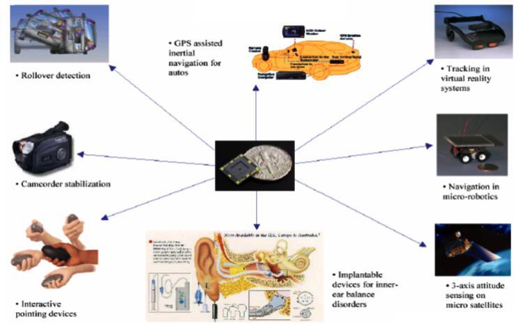
11 MEMS: Products Microwave and Wireless Switches Filters Components Power sensors Pressure MAP sensors Microphones Medical and Biological Lab on a Chip DNA analysis Chem/Bio Detection Drug Delivery Ink Jet Printers Thermal Ink-Jets Inertial Accelerometers Gyroscopes Optics Projection Displays Laser Printers Switching Networks Tunable Lasers Filters 11

 and temperature")


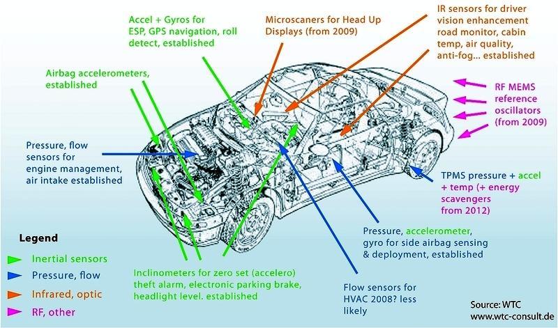
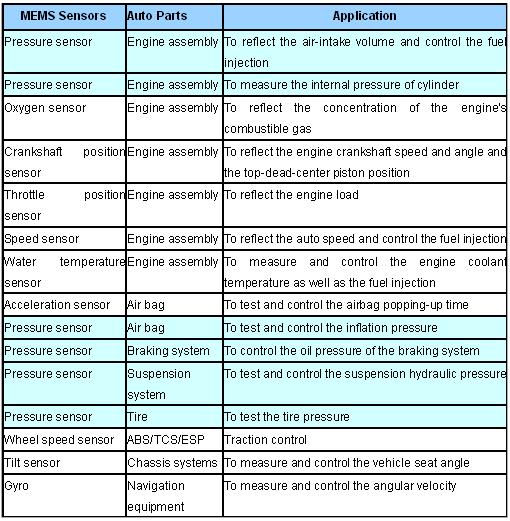
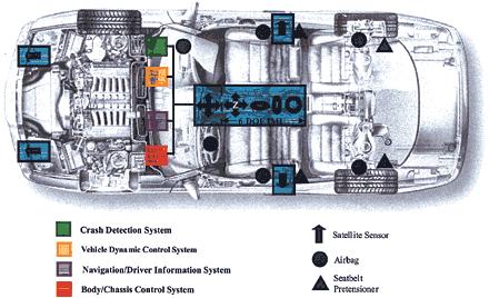
12 MEMS: Industrial applications Automotive Industry: pressure sensors (engine oil pressure, vacuum pressure, fuel injection pressure, tire pressure, stored air bag pressure), accelerometers (triggering of air bag, locking seat belt) and temperature sensors (to monitor oil, antifreeze and air temperature) Controls for Industry or Home: sensors to measure external environment and actuators for adjustment Instrumentation and Control Industry uses MEMS devices which sense pressure, temperature, acceleration and proximity. 12
13 MEMS: Manufactures 13
14 Applications: Automotive 14
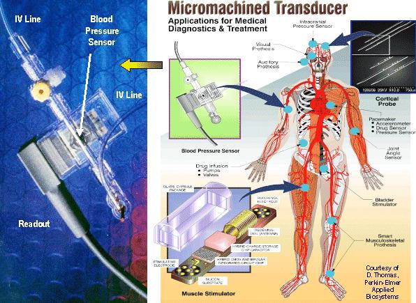
15 Applications: Medicine 15
16 MEMS: Biotechnology Examples of MEMS applications in Biotechnology: Polymerase Chain Reaction (PCR) microsystems for DNA amplification and identification; Enzyme linked immunosorbent assay (ELISA); Capillary electrophoresis; Electroporation; Micromachined Scanning Tunneling Microscopes (STMs); Biochips for detection of hazardous chemical and biological agents. Microsystems for high-throughput drug screening and selection. 16

17 Applications: Aeronautics Pressure sensor belt on jet planes 17

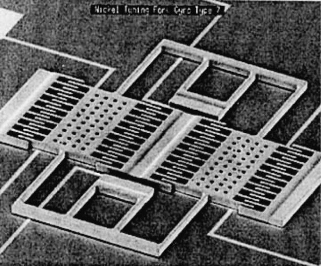

18 Applications: Gyroscopes Micromachined gyroscopes applications. 18

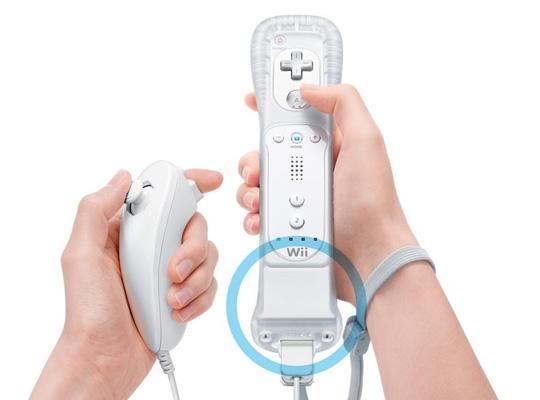
19 Applications: Nintendo Wii 19


20 Applications: smart-phone 20
21 MEMS: Resources Books: Microsensors Principles and applications J. W. Gardner 1994, Wiley Micromechanics and MEMS Classic and Seminal Papers to 1990 Edited by William S.Trimmer 1997, IEEE PRESS Fundamentals of Microfabrication M. Madou 1997, CRC Press LLC Micromachined Transducers Sourcebook G. T. A. Kovacs 1998, McGraw-Hill Micro Mechanical Systems Principles and Technology Handbook of Sensors and Actuators, Vol.6 T. Fukuda and W. Menz 1998, ELSEVIER Scientific Journals: IEEE/ASME, Journal of Microelectromechanical Systems Elsevier, Sensors and Actuators IoP, Journal of Micromechanics and Microengineering IEEE, Sensors Journal International Scientific Conferences: IEEE MEMS SPIE Smart Structures and Systems Smart electronics and MEMS Eurosensors IEEE Sensors Websites:

22 MEMS: Fabrication MEMS are fabricated using integrated circuits (ICs) compatible batch-processing techniques and silicon-based technologies. 22

23 MEMS fabrication: Advantages 23
24 MEMS and Microelectronics (IC) Interactions with the environment: Microelectronics generally interacts with "information" such as signals or streams of electrons; MEMS interacts with a wide variety of physical quantities (fluid, acceleration, optics, electromagnetic waves, etc.). Structural dimensionality: Microelectronic systems are "predominantly" two-dimensional (the structure is built in a layer thinner than the thickness of the entire substrate). MEMS are inherently three-dimensional (Some properties are developed for more than 100 micrometers in depth). Fabrication technology: Although Microsystems were originally developed on the same silicon substrates for microelectronic circuits, today other substrates and different technologies are adopted. 24
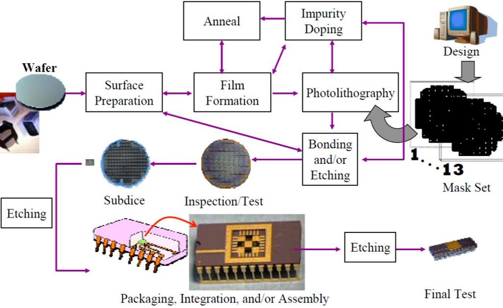
25 MEMS: Fabrication 25
 Bulk Micromachining (structures made")
 Patterning and shaping, in the above techniques, is usually accomplishedthrough: Photolithography")
26 MEMS: Fabrication MEMS fabrication techniques can be categorized as follows: Surface Micromachining (structures made from single or multiple films that are patterned) Bulk Micromachining (structures made from chemically etched bulk material) Micromolding (structures made using molds, stereo lithography, milling) Patterning and shaping, in the above techniques, is usually accomplishedthrough: Photolithography Chemical Etching 26

27 Silicon as structural material The monocrystalline silicon structure has a face-centered cubic (diamondlattice, lattice constant = 5.43 Å). Each atom is placed at the center of a tetrahedron and is associated with covalent bond, four equidistant atoms. To allow easy identification of the crystallographic planes, "Miller Indices" (inverse of the intersection between the plane and the unit vectors of the reference system) are used. The surface of the silicon wafer is contained in a three main floors. Conventions for the recognition of the type of substrate are adopted. 27
28 Other materials for MEMS Polycrystalline Silicon or Polysilicon: used as both a strucutral material and conductive material, piezo-resistive properties. Silicon Dioxide (SiO 2 ): used as an electrical isolant and in some cases as a structural or sacrificial layer. Silicon Nitride (Si 3 N 4 ): used as an electrical isolant and in some cases as a structural or sacrificial layer. Metals (Alluminium, Platinum, Gold, Nickel, Tungsten, etc ): used as an electrical conductors, optical reflective, thermo-mechanical transducer and in some cases as structural materials. PZT: used for piezo-electrical conversions. 28
29 Silicon micro-fabrication processes Classification by type of material Metal (Al, Au, Cu, Ti, Ni, Pt, etc.) Non-metal inorganic material (SiO 2, Si 3 N 4, SiC, compound nitride materials) Classification by material addiction/subtraction Deposition process Photoresist Metal evaporation Oxidation Sputtering CVD Anisotropic etching Isotropic etching Bulk/film etching Sacrifical Classification by process temperature Examples: Oxidation: C Annealing: C Si 3 N 4 LPCVD: 780 C Polysilicon LPCVD: C Low temp. oxide LPCVD: about 550 C Plasma deposition: about 350 C Spin-coating: room temperature Classification by size: Thin film (thickness < 10 μm) Thick film Bulk 29
30 Deposition processes Addictive processes to deposit material on a layer: Spin-on films Polyimide (PI), Photoresist (PR) Spin-on glass (SOG) Physical Vapor Deposition (PVD) Evaporation Sputtering Chemical Vapor Deposition (CVD) Thermal Oxidation (wet/dry) CVD (Atmopheric Pressure) Low Pressure CVD (LPCVD) Plasma Enhanced CVD (PECVD) 30
31 Deposition processes: Spin-on films Spin-on films or Spin Casting Thin film material is dissolved in a volatile liquid solvent, spin coated onto a substrate to form films due to centrifugal force. Examples: Polyimide (PI), Photoresist (PR) Spin-on glass (SOG) 31

32 Deposition processes: PVD Physical Vapor Deposition (PVD) Evaporation The material to be deposited is heated by resistive, inductive, or electron beam and led to gaseous state. Condensation of the evaporated gas, on high-vacuum chambers, induces the deposition of the layer. Sputtering High-energy ion beams (plasma) are used to remove atoms from the surface of the source material (material to be deposited) to create a layer. 32

33 Deposition processes: CVD Chemical Vapor Deposition (CVD) Deposition on a substrate of a solid layer as a result of a chemical reaction between the substrate material and the gases in the atmosphere. Thermal Oxidation (wet/dry) CVD (Atmopheric Pressure) Low Pressure CVD (LPCVD) Plasma Enhanced CVD (PECVD) CVD - LPCDV PECVD 33
 uniform deposition of a layer of structural material where to tranfer the pattern, (b) deposition of photoresist, (c) selective exposure to UV light through mask")
34 Photolithography Technique of transferring a geometric two-dimensional pattern to a surface. It is divided into six phases: (a) uniform deposition of a layer of structural material where to tranfer the pattern, (b) deposition of photoresist, (c) selective exposure to UV light through mask layout, (d) selective removal of the photoresist (e) selective removal of structural material, (f) final removal of residual photoresist. 34
 used in the process of photolithography affects the definition of the layout masks.")

35 Photolithography: Layout Masks Layout masks define the geometry / pattern and size of the device. The type of photoresist (positive/negative) used in the process of photolithography affects the definition of the layout masks. Positive Photoresist: becomes soluble in exposed areas the material is etched in the areas covered by the mask transferred pattern is the same of the mask. Negative Photoresist: become insoluble in the exposed areas material is excavated in the areas uncovered by the mask transferred pattern is the negative of the mask. 35

.")
 Bulk etching (removal of part of the substrate) By surface: Top (etch from the upper surface of the")
36 Substraction processes Etching process: process of selectively removing material The selectivity is determined by using appropriate photolithographic masks together with masking materials. The selectivity with respect to the materials is characterized by the etch-rate (rate etching, for a given chemical etchant, is characteristic of the material). Classification of etching processes By depth: Surface etching (removal of thin films from the surface of the wafer) Bulk etching (removal of part of the substrate) By surface: Top (etch from the upper surface of the wafer) Bottom (etch from the bottom surface of the wafer) By etch-rate direction: Isotropic Anisotropic 36

 in the liquid phase.")

37 Wet etch by KOH Dry etch by RIE Substraction processes: wet/dry etch Wet etch: removal by chemical attack (by KOH or TMAH) in the liquid phase. Dry etch: material removal occurs by reaction with a gas in "vapor-phase" or "plasma-phase" etching. 37


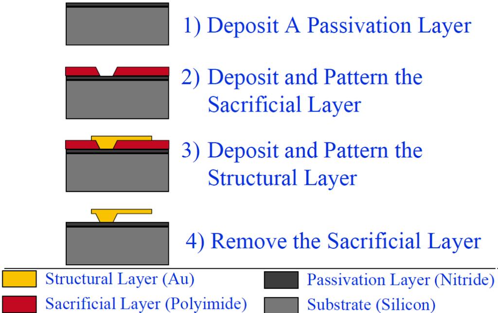
38 Sacrificial etching Sacrificial layer Substrate 1 4 Polysilicon
39 Tipical micro-fabrication process Starting Silicon Bulk Substrate Starting silicon substrate for supporting purpose Material Deposition Deposition of material with a defined thickness Photolitography Two-dimensional patterning of the previously deposited material Final Etching Final etching to realize suspended structures 39
40 Surface Micromachining 40

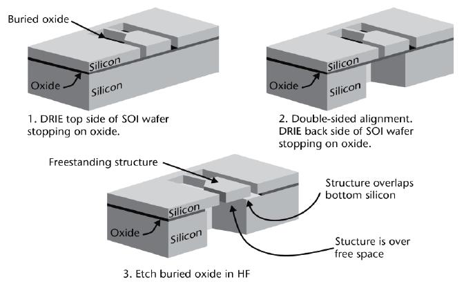
41 Bulk Micromachining Example on Silicon-On-Insulator (SOI) substrate 41
Chapter 2 OVERVIEW OF MEMS
 6 Chapter 2 OVERVIEW OF MEMS 2.1 MEMS and Microsystems The term MEMS is an abbreviation of microelectromechanical system. MEMS contains components ofsizes in 1 micrometer to 1 millimeter. The core element
Today s Class. Materials for MEMS
 Lecture 2: VLSI-based Fabrication for MEMS: Fundamentals Prasanna S. Gandhi Assistant Professor, Department of Mechanical Engineering, Indian Institute of Technology, Bombay, Recap: Last Class What is
General Introduction to Microstructure Technology p. 1 What is Microstructure Technology? p. 1 From Microstructure Technology to Microsystems
 General Introduction to Microstructure Technology p. 1 What is Microstructure Technology? p. 1 From Microstructure Technology to Microsystems Technology p. 9 The Parallels to Microelectronics p. 15 The
EE 5344 Introduction to MEMS. CHAPTER 3 Conventional Si Processing
 3. Conventional licon Processing Micromachining, Microfabrication. EE 5344 Introduction to MEMS CHAPTER 3 Conventional Processing Why silicon? Abundant, cheap, easy to process. licon planar Integrated
Physical Vapor Deposition (PVD) Zheng Yang
 Zheng Yang") Physical Vapor Deposition (PVD) Zheng Yang ERF 3017, email: yangzhen@uic.edu Page 1 Major Fabrication Steps in MOS Process Flow UV light Mask oxygen Silicon dioxide photoresist exposed photoresist oxide
Physical Vapor Deposition (PVD) Zheng Yang ERF 3017, email: yangzhen@uic.edu Page 1 Major Fabrication Steps in MOS Process Flow UV light Mask oxygen Silicon dioxide photoresist exposed photoresist oxide
Manufacturing Technologies for MEMS and SMART SENSORS
 4 Manufacturing Technologies for MEMS and SMART SENSORS Dr. H. K. Verma Distinguished Professor (EEE) Sharda University, Greater Noida (Formerly: Deputy Director and Professor of Instrumentation Indian
EECS130 Integrated Circuit Devices
 EECS130 Integrated Circuit Devices Professor Ali Javey 9/13/2007 Fabrication Technology Lecture 1 Silicon Device Fabrication Technology Over 10 15 transistors (or 100,000 for every person in the world)
PETER PAZMANY CATHOLIC UNIVERSITY Consortium members SEMMELWEIS UNIVERSITY, DIALOG CAMPUS PUBLISHER
 PETER PAZMANY CATHOLIC UNIVERSITY SEMMELWEIS UNIVERSITY Development of Complex Curricula for Molecular Bionics and Infobionics Programs within a consortial* framework** Consortium leader PETER PAZMANY
MEMS Fabrication. Beyond Integrated Circuits. MEMS Basic Concepts
 MEMS Fabrication Beyond Integrated Circuits MEMS Basic Concepts Uses integrated circuit fabrication techniques to make mechanical as well as electrical components on a single chip. Small size 1µm 1mm Typically
Solid State Sensors. Microfabrication 8/22/08 and 8/25/08
 Solid State Sensors Microfabrication 8/22/08 and 8/25/08 Purpose of This Material To introduce the student to microfabrication techniques as used to fabricate MEMS Sensors Understand concepts not specifics
PHYS 534 (Fall 2008) Process Integration OUTLINE. Examples of PROCESS FLOW SEQUENCES. >Surface-Micromachined Beam
 Process Integration OUTLINE. Examples of PROCESS FLOW SEQUENCES. >Surface-Micromachined Beam") PHYS 534 (Fall 2008) Process Integration Srikar Vengallatore, McGill University 1 OUTLINE Examples of PROCESS FLOW SEQUENCES >Semiconductor diode >Surface-Micromachined Beam Critical Issues in Process
PHYS 534 (Fall 2008) Process Integration Srikar Vengallatore, McGill University 1 OUTLINE Examples of PROCESS FLOW SEQUENCES >Semiconductor diode >Surface-Micromachined Beam Critical Issues in Process
IC/MEMS Fabrication - Outline. Fabrication
 IC/MEMS Fabrication - Outline Fabrication overview Materials Wafer fabrication The Cycle: Deposition Lithography Etching Fabrication IC Fabrication Deposition Spin Casting PVD physical vapor deposition
Surface micromachining and Process flow part 1
 Surface micromachining and Process flow part 1 Identify the basic steps of a generic surface micromachining process Identify the critical requirements needed to create a MEMS using surface micromachining
Chapter 3 Silicon Device Fabrication Technology
 Chapter 3 Silicon Device Fabrication Technology Over 10 15 transistors (or 100,000 for every person in the world) are manufactured every year. VLSI (Very Large Scale Integration) ULSI (Ultra Large Scale
Welcome MNT Conference 1 Albuquerque, NM - May 2010
 Welcome MNT Conference 1 Albuquerque, NM - May 2010 Introduction to Design Outline What is MEMs Design General Considerations Application Packaging Process Flow What s available Sandia SUMMiT Overview
Mostafa Soliman, Ph.D. May 5 th 2014
 Mostafa Soliman, Ph.D. May 5 th 2014 Mostafa Soliman, Ph.D. 1 Basic MEMS Processes Front-End Processes Back-End Processes 2 Mostafa Soliman, Ph.D. Wafers Deposition Lithography Etch Chips 1- Si Substrate
Thomas M. Adams Richard A. Layton. Introductory MEMS. Fabrication and Applications. Springer
 Thomas M. Adams Richard A. Layton Introductory MEMS Fabrication and Applications Springer Contents Preface xiü Part I Fabrication Chapter 1: Introduction 3 1.1 What are MEMS? 3 1.2 Why MEMS? 4 1.2.1. Low
Mikrosensorer. Microfabrication 1
 Mikrosensorer Microfabrication 1 Literature Introductory MEMS Fabrication and Applications Thomas M. Adams and Richard A. Layton Available as ebook on http://www.lub.lu.se/en/search/lubsearch.html This
Micromachining AMT 2505
 Micromachining AMT 2505 Shanmuga Raja.B (BVB0912004) Module leader : Mr. Raja Hussain Introduction Micromachining are inherently connected to the evolution of Micro Electro Mechanical Systems (MEMS). Decades
Surface Micromachining
 Surface Micromachining Micro Actuators, Sensors, Systems Group University of Illinois at Urbana-Champaign Outline Definition of surface micromachining Most common surface micromachining materials - polysilicon
Preface Preface to First Edition
 Contents Foreword Preface Preface to First Edition xiii xv xix CHAPTER 1 MEMS: A Technology from Lilliput 1 The Promise of Technology 1 What Are MEMS or MST? 2 What Is Micromachining? 3 Applications and
INF5490 RF MEMS. LN02: MEMS Fabrication. Spring 2012, Oddvar Søråsen Department of Informatics, UoO
 INF5490 RF MEMS LN02: MEMS Fabrication Spring 2012, Oddvar Søråsen Department of Informatics, UoO 1 Micromachining Today s lecture Important process steps General Summary: MEMS-specific steps Examples
Lecture 5: Micromachining
 MEMS: Fabrication Lecture 5: Micromachining Prasanna S. Gandhi Assistant Professor, Department of Mechanical Engineering, Indian Institute of Technology, Bombay, Recap: Last Class E-beam lithography X-ray
Metallization deposition and etching. Material mainly taken from Campbell, UCCS
 Metallization deposition and etching Material mainly taken from Campbell, UCCS Application Metallization is back-end processing Metals used are aluminum and copper Mainly involves deposition and etching,
Lect. 2: Basics of Si Technology
 Unit processes Thin Film Deposition Etching Ion Implantation Photolithography Chemical Mechanical Polishing 1. Thin Film Deposition Layer of materials ranging from fractions of nanometer to several micro-meters
Dr. Lynn Fuller Webpage:
 ROCHESTER INSTITUTE OF TECHNOLOGY MICROELECTRONIC ENGINEERING Microelectromechanical Systems (MEMs) Process Integration Dr. Lynn Fuller Webpage: http://people.rit.edu/lffeee 82 Lomb Memorial Drive Rochester,
Micromachining vs. Soft Fabrication
 Introduction to BioMEMS & Medical Microdevices Silicon Microfabrication Part 1 Companion lecture to the textbook: Fundamentals of BioMEMS and Medical Microdevices, by Prof., http://saliterman.umn.edu/
Review of CMOS Processing Technology
 - Scaling and Integration Moore s Law Unit processes Thin Film Deposition Etching Ion Implantation Photolithography Chemical Mechanical Polishing 1. Thin Film Deposition Layer of materials ranging from
5.8 Diaphragm Uniaxial Optical Accelerometer
 5.8 Diaphragm Uniaxial Optical Accelerometer Optical accelerometers are based on the BESOI (Bond and Etch back Silicon On Insulator) wafers, supplied by Shin-Etsu with (100) orientation, 4 diameter and
Chapter 4 Fabrication Process of Silicon Carrier and. Gold-Gold Thermocompression Bonding
 Chapter 4 Fabrication Process of Silicon Carrier and Gold-Gold Thermocompression Bonding 4.1 Introduction As mentioned in chapter 2, the MEMs carrier is designed to integrate the micro-machined inductor
ME 189 Microsystems Design and Manufacture. Chapter 9. Micromanufacturing
 ME 189 Microsystems Design and Manufacture Chapter 9 Micromanufacturing This chapter will offer an overview of the application of the various fabrication techniques described in Chapter 8 in the manufacturing
Materials for MEMS. Dr. Yael Hanein. 11 March 2004 Materials Applications Yael Hanein
 Materials for MEMS Dr. Yael Hanein Materials for MEMS MEMS (introduction) Materials used in MEMS Material properties Standard MEMS processes MEMS The world s smallest guitar is about 10 micrometers long
Czochralski Crystal Growth
 Czochralski Crystal Growth Crystal Pulling Crystal Ingots Shaping and Polishing 300 mm wafer 1 2 Advantage of larger diameter wafers Wafer area larger Chip area larger 3 4 Large-Diameter Wafer Handling
Surface Micromachining
 Surface Micromachining Outline Introduction Material often used in surface micromachining Material selection criteria in surface micromachining Case study: Fabrication of electrostatic motor Major issues
Evolution of MEMS Technology
 Evolution of MEMS Technology 1 Raksha Sahadev Hukkeri, 2 Shreya Madapurmath, 3 Shreelekha Navale 1,2,3 UG Student, Department of ECE, SDMCET Dharwad Abstract Micro-Electro-Mechanical Systems (MEMS) is
There are basically two approaches for bulk micromachining of. silicon, wet and dry. Wet bulk micromachining is usually carried out
 57 Chapter 3 Fabrication of Accelerometer 3.1 Introduction There are basically two approaches for bulk micromachining of silicon, wet and dry. Wet bulk micromachining is usually carried out using anisotropic
Basic&Laboratory& Materials&Science&and&Engineering& Micro&Electromechanical&Systems&& (MEMS)&
&") Basic&Laboratory& Materials&Science&and&Engineering& Micro&Electromechanical&Systems&& (MEMS)& M105& As of: 27.10.2011 1 Introduction... 2 2 Materials used in MEMS fabrication... 2 3 MEMS fabrication processes...
Basic&Laboratory& Materials&Science&and&Engineering& Micro&Electromechanical&Systems&& (MEMS)& M105& As of: 27.10.2011 1 Introduction... 2 2 Materials used in MEMS fabrication... 2 3 MEMS fabrication processes...
FABRICATION PROCESSES FOR MAGNETIC MICROACTUATORS WITH POLYSILICON FLEXURES. Jack W. Judy and Richard S. Muller
 FABRICATION PROCESSES FOR MAGNETIC MICROACTUATORS WITH POLYSILICON FLEXURES Jack W. Judy and Richard S. Muller Berkeley Sensor & Actuator Center (BSAC) Department of EECS, University of California, Berkeley,
MEMSAND MICROSYSTEMS Design, Manufacture, and Nanoscale Engineering
 MEMSAND MICROSYSTEMS Design, Manufacture, and Nanoscale Engineering Second Edition TAI-RAN HSU Microsystems Design and Packaging Laboratory Department of Mechanical and Aerospace Engineering San Jose State
Fabrication Technology, Part II
 EEL5225: Principles of MEMS Transducers (Fall 2003) Fabrication Technology, Part II Agenda: Process Examples TI Micromirror fabrication process SCREAM CMOS-MEMS processes Wafer Bonding LIGA Reading: Senturia,
6.777J/2.732J Design and Fabrication of Microelectromechanical Devices Spring Term Solution to Problem Set 2 (16 pts)
") 6.777J/2.732J Design and Fabrication of Microelectromechanical Devices Spring Term 2007 By Brian Taff (Adapted from work by Feras Eid) Solution to Problem Set 2 (16 pts) Issued: Lecture 4 Due: Lecture
6.777J/2.732J Design and Fabrication of Microelectromechanical Devices Spring Term 2007 By Brian Taff (Adapted from work by Feras Eid) Solution to Problem Set 2 (16 pts) Issued: Lecture 4 Due: Lecture
Knowledge Probe Deposition PK Activities. Participant Guide
 Deposition Overview for Microsystems Knowledge Probe Deposition PK Activities Participant Guide www.scme-nm.org University of New Mexico MEMS Fabrication Topic Deposition Overview for Microsystems Learning
ELEC 3908, Physical Electronics, Lecture 4. Basic Integrated Circuit Processing
 ELEC 3908, Physical Electronics, Lecture 4 Basic Integrated Circuit Processing Lecture Outline Details of the physical structure of devices will be very important in developing models for electrical behavior
Semiconductor Device Fabrication
 5 May 2003 Review Homework 6 Semiconductor Device Fabrication William Shockley, 1945 The network before the internet Bell Labs established a group to develop a semiconductor replacement for the vacuum
Influence of Underlayer on Crystallography and Roughness of Aluminum Nitride Thin Film Reactively Sputtered by Ion-Beam Kaufman Source
 Influence of Underlayer on Crystallography and Roughness of Aluminum Nitride Thin Film Reactively Sputtered by Ion-Beam Kaufman Source GABLECH Imrich 1,*, SVATOŠ Vojtěch 1,, PRÁŠEK Jan 1,, HUBÁLEK Jaromír
EE C245 ME C218 Introduction to MEMS Design Fall 2011
 Lecture Outline EE C245 ME C218 Introduction to MEMS Design Fall 2011 Prof. Clark T.-C. Nguyen Dept. of Electrical Engineering & Computer Sciences University of California at Berkeley Berkeley, CA 94720
Lecture 10: MultiUser MEMS Process (MUMPS)
") MEMS: Fabrication Lecture 10: MultiUser MEMS Process (MUMPS) Prasanna S. Gandhi Assistant Professor, Department of Mechanical Engineering, Indian Institute of Technology, Bombay, 1 Recap Various VLSI based
MEMS: Fabrication Lecture 10: MultiUser MEMS Process (MUMPS) Prasanna S. Gandhi Assistant Professor, Department of Mechanical Engineering, Indian Institute of Technology, Bombay, 1 Recap Various VLSI based
PRESSURE SENSOR MODEL ACTIVITY. Pressure Sensor Model Activity
 PRESSURE SENSOR MODEL ACTIVITY Pressure Sensor Model Activity Unit Overview This activity uses household materials to build a pressure sensor Wheatstone Bridge sensing circuit Flexible diaphragm Reference
Microstructure of Electronic Materials. Amorphous materials. Single-Crystal Material. Professor N Cheung, U.C. Berkeley
 Microstructure of Electronic Materials Amorphous materials Single-Crystal Material 1 The Si Atom The Si Crystal diamond structure High-performance semiconductor devices require defect-free crystals 2 Crystallographic
PROCESS FLOW AN INSIGHT INTO CMOS FABRICATION PROCESS
 Contents: VI Sem ECE 06EC63: Analog and Mixed Mode VLSI Design PROCESS FLOW AN INSIGHT INTO CMOS FABRICATION PROCESS 1. Introduction 2. CMOS Fabrication 3. Simplified View of Fabrication Process 3.1 Alternative
CMOS Manufacturing process. Design rule set
 CMOS Manufacturing process Circuit design Set of optical masks Fabrication process Circuit designer Design rule set Process engineer All material: Chap. 2 of J. Rabaey, A. Chandrakasan, B. Nikolic, Digital
Fabrication Process. Crystal Growth Doping Deposition Patterning Lithography Oxidation Ion Implementation CONCORDIA VLSI DESIGN LAB
 Fabrication Process Crystal Growth Doping Deposition Patterning Lithography Oxidation Ion Implementation 1 Fabrication- CMOS Process Starting Material Preparation 1. Produce Metallurgical Grade Silicon
Silicon Microfabrication Part 2
 Introduction to BioMEMS & Medical Microdevices Silicon Microfabrication Part 2 Companion lecture to the textbook: Fundamentals of BioMEMS and Medical Microdevices, by Prof., http://saliterman.umn.edu/
Overview. Silicon Microfabrication Part 2. Introduction to BioMEMS & Medical Microdevices
 Introduction to BioMEMS & Medical Microdevices Silicon Microfabrication Part 2 Companion lecture to the textbook: Fundamentals of BioMEMS and Medical Microdevices, by Prof., http://saliterman.umn.edu/
Single crystal silicon supported thin film micromirrors for optical applications
 Single crystal silicon supported thin film micromirrors for optical applications Zhimin J. Yao* Noel C. MacDonald Cornell University School of Electrical Engineering and Cornell Nanofabrication Facility
Semiconductor Manufacturing Process 10/11/2005
 Semiconductor Manufacturing Process 10/11/2005 Photolithography Oxidation CVD PVD Photolithography The purpose of photolithography is to imprint the desired pattern of a micro component on a substrate,
Lecture #18 Fabrication OUTLINE
 Transistors on a Chip Lecture #18 Fabrication OUTLINE IC Fabrication Technology Introduction the task at hand Doping Oxidation Thin-film deposition Lithography Etch Lithography trends Plasma processing
Micro-Electro-Mechanical Systems (MEMS) Fabrication. Special Process Modules for MEMS. Principle of Sensing and Actuation
 Fabrication. Special Process Modules for MEMS. Principle of Sensing and Actuation") Micro-Electro-Mechanical Systems (MEMS) Fabrication Fabrication Considerations Stress-Strain, Thin-film Stress, Stiction Special Process Modules for MEMS Bonding, Cavity Sealing, Deep RIE, Spatial forming
Micro-Electro-Mechanical Systems (MEMS) Fabrication Fabrication Considerations Stress-Strain, Thin-film Stress, Stiction Special Process Modules for MEMS Bonding, Cavity Sealing, Deep RIE, Spatial forming
Microelectronics. Integrated circuits. Introduction to the IC technology M.Rencz 11 September, Expected decrease in line width
 Microelectronics Introduction to the IC technology M.Rencz 11 September, 2002 9/16/02 1/37 Integrated circuits Development is controlled by the roadmaps. Self-fulfilling predictions for the tendencies
Nanoelectronics Fabrication Facility
 Nanoelectronics Fabrication Facility Contents Introduction 2 Mask Making Module 4 Photolithography Module 6 Wet Etching and CMP Module 8 Dry Etching and Sputtering Module 10 Thermal Process and Implantation
Chapter 3 CMOS processing technology
 Chapter 3 CMOS processing technology (How to make a CMOS?) Si + impurity acceptors(p-type) donors (n-type) p-type + n-type => pn junction (I-V) 3.1.1 (Wafer) Wafer = A disk of silicon (0.25 mm - 1 mm thick),
Lecture 22: Integrated circuit fabrication
 Lecture 22: Integrated circuit fabrication Contents 1 Introduction 1 2 Layering 4 3 Patterning 7 4 Doping 8 4.1 Thermal diffusion......................... 10 4.2 Ion implantation.........................
Chemical Vapor Deposition
 Chemical Vapor Deposition ESS4810 Lecture Fall 2010 Introduction Chemical vapor deposition (CVD) forms thin films on the surface of a substrate by thermal decomposition and/or reaction of gas compounds
Micro-Electro-Mechanical Systems (MEMS) Fabrication. Special Process Modules for MEMS. Principle of Sensing and Actuation
 Fabrication. Special Process Modules for MEMS. Principle of Sensing and Actuation") Micro-Electro-Mechanical Systems (MEMS) Fabrication Fabrication Considerations Stress-Strain, Thin-film Stress, Stiction Special Process Modules for MEMS Bonding, Cavity Sealing, Deep RIE, Spatial forming
Micro-Electro-Mechanical Systems (MEMS) Fabrication Fabrication Considerations Stress-Strain, Thin-film Stress, Stiction Special Process Modules for MEMS Bonding, Cavity Sealing, Deep RIE, Spatial forming
4/10/2012. Introduction to Microfabrication. Fabrication
 Introduction to Microfabrication Fabrication 1 MEMS Fabrication Flow Basic Process Flow in Micromachining Nadim Maluf, An introduction to Microelectromechanical Systems Engineering 2 Thin Film Deposition
PHYSICAL ELECTRONICS(ECE3540) Brook Abegaz, Tennessee Technological University, Fall 2013
 Brook Abegaz, Tennessee Technological University, Fall 2013") PHYSICAL ELECTRONICS(ECE3540) Brook Abegaz, Tennessee Technological University, Fall 2013 1 Chapter 1 The Crystal Structure of Solids Physical Electronics: Includes aspects of the physics of electron movement
PHYSICAL ELECTRONICS(ECE3540) Brook Abegaz, Tennessee Technological University, Fall 2013 1 Chapter 1 The Crystal Structure of Solids Physical Electronics: Includes aspects of the physics of electron movement
Multiple-height Microstructures Fabricated by ICP-RIE and Embedded Masking Layers
 Paper Multiple-height Microstructures Fabricated by ICP-RIE and Embedded Masking Layers Student Member Makoto Mita (IIS., Univ. of Tokyo & CREST/JST ) Student Member Yoshio Mita (IIS., Univ. of Tokyo)
Wafer (1A) Young Won Lim 4/30/13
 Young Won Lim 4/30/13") Copyright (c) 2011-2013 Young W. Lim. Permission is granted to copy, distribute and/or modify this document under the terms of the GNU Free Documentation License, Version 1.2 or any later version published
Copyright (c) 2011-2013 Young W. Lim. Permission is granted to copy, distribute and/or modify this document under the terms of the GNU Free Documentation License, Version 1.2 or any later version published
Smarter sensing solutions
 Easy access to microsystems production through contract manufacturing services Espoo, Finland June 14th 2011 Smarter sensing solutions Colibrys Foundry presentation: Sean Neylon Business Model The Colibrys
Lecture 3: Integrated Processes
 Lecture 3: Integrated Processes Single-Crystal Silicon Process Integration Polysilicon Micromachining Process Integrated CMOS Micromachining Process ENE 5400, Spring 2004 1 Single Crystal Silicon ENE 5400,
Micro-Scale Engineering I Microelectromechanical Systems (MEMS) Y. C. Lee
 Y. C. Lee") Micro-Scale Engineering I Microelectromechanical Systems (MEMS) Y. C. Lee Department of Mechanical Engineering University of Colorado Boulder, CO 80309-0427 leeyc@colorado.edu September 2, 2008 1 Three
Micro-Scale Engineering I Microelectromechanical Systems (MEMS) Y. C. Lee Department of Mechanical Engineering University of Colorado Boulder, CO 80309-0427 leeyc@colorado.edu September 2, 2008 1 Three
Fabrication Technology, Part I
 EEL5225: Principles of MEMS Transducers (Fall 2003) Fabrication Technology, Part I Agenda: Oxidation, layer deposition (last lecture) Lithography Pattern Transfer (etching) Impurity Doping Reading: Senturia,
Lecture 19 Microfabrication 4/1/03 Prof. Andy Neureuther
 EECS 40 Spring 2003 Lecture 19 Microfabrication 4/1/03 Prof. ndy Neureuther How are Integrated Circuits made? Silicon wafers Oxide formation by growth or deposition Other films Pattern transfer by lithography
MEMS prototyping using RF sputtered films
 Indian Journal of Pure & Applied Physics Vol. 45, April 2007, pp. 326-331 MEMS prototyping using RF sputtered films Sudhir Chandra, Vivekanand Bhatt, Ravindra Singh, Preeti Sharma & Prem Pal* Centre for
Fabrication and Layout
 ECEN454 Digital Integrated Circuit Design Fabrication and Layout ECEN 454 3.1 A Glimpse at MOS Device Polysilicon Aluminum ECEN 475 4.2 1 Material Classification Insulators Glass, diamond, silicon oxide
Microfabrication of Integrated Circuits
 Microfabrication of Integrated Circuits OUTLINE History Basic Processes Implant; Oxidation; Photolithography; Masks Layout and Process Flow Device Cross Section Evolution Lecture 38, 12/05/05 Reading This
The Physical Structure (NMOS)
") The Physical Structure (NMOS) Al SiO2 Field Oxide Gate oxide S n+ Polysilicon Gate Al SiO2 SiO2 D n+ L channel P Substrate Field Oxide contact Metal (S) n+ (G) L W n+ (D) Poly 1 3D Perspective 2 3 Fabrication
The Physical Structure (NMOS) Al SiO2 Field Oxide Gate oxide S n+ Polysilicon Gate Al SiO2 SiO2 D n+ L channel P Substrate Field Oxide contact Metal (S) n+ (G) L W n+ (D) Poly 1 3D Perspective 2 3 Fabrication
Available online at ScienceDirect. Procedia Materials Science 6 (2014 )
") Available online at www.sciencedirect.com ScienceDirect Procedia Materials Science 6 (2014 ) 1170 1177 3rd International Conference on Materials Processing and Characterisation (ICMPC 2014) Micro Machining
Available online at www.sciencedirect.com ScienceDirect Procedia Materials Science 6 (2014 ) 1170 1177 3rd International Conference on Materials Processing and Characterisation (ICMPC 2014) Micro Machining
Supporting Information: Model Based Design of a Microfluidic. Mixer Driven by Induced Charge Electroosmosis
 Supporting Information: Model Based Design of a Microfluidic Mixer Driven by Induced Charge Electroosmosis Cindy K. Harnett, Yehya M. Senousy, Katherine A. Dunphy-Guzman #, Jeremy Templeton * and Michael
3. Overview of Microfabrication Techniques
 3. Overview of Microfabrication Techniques The Si revolution First Transistor Bell Labs (1947) Si integrated circuits Texas Instruments (~1960) Modern ICs More? Check out: http://www.pbs.org/transistor/background1/events/miraclemo.html
Complexity of IC Metallization. Early 21 st Century IC Technology
 EECS 42 Introduction to Digital Electronics Lecture # 25 Microfabrication Handout of This Lecture. Today: how are Integrated Circuits made? Silicon wafers Oxide formation by growth or deposition Other
Micro-Electro-Mechanical Systems (MEMS) Fabrication. Special Process Modules for MEMS. Principle of Sensing and Actuation
 Fabrication. Special Process Modules for MEMS. Principle of Sensing and Actuation") Micro-Electro-Mechanical Systems (MEMS) Fabrication Fabrication Considerations Stress-Strain, Thin-film Stress, Stiction Special Process Modules for MEMS Bonding, Cavity Sealing, Deep RIE, Spatial forming
Micro-Electro-Mechanical Systems (MEMS) Fabrication Fabrication Considerations Stress-Strain, Thin-film Stress, Stiction Special Process Modules for MEMS Bonding, Cavity Sealing, Deep RIE, Spatial forming
Tackling the optical interconnection challenge for the Integrated Photonics Revolution
 Tackling the optical interconnection challenge for the Integrated Photonics Revolution Dr. Ir. TU Delft, Precision and Microsystems Engineering m.tichem@tudelft.nl Microfabrication and MEMS Si microfabrication
Microfabrication of Heterogeneous, Optimized Compliant Mechanisms SUNFEST 2001 Luo Chen Advisor: Professor G.K. Ananthasuresh
 Microfabrication of Heterogeneous, Optimized Compliant Mechanisms SUNFEST 2001 Luo Chen Advisor: Professor G.K. Ananthasuresh Fig. 1. Single-material Heatuator with selective doping on one arm (G.K. Ananthasuresh)
Supporting Information
 Supporting Information Fast-Response, Sensitivitive and Low-Powered Chemosensors by Fusing Nanostructured Porous Thin Film and IDEs-Microheater Chip Zhengfei Dai,, Lei Xu,#,, Guotao Duan *,, Tie Li *,,
Introduction to Micro/Nano Fabrication Techniques. Date: 2015/05/22 Dr. Yi-Chung Tung. Fabrication of Nanomaterials
 Introduction to Micro/Nano Fabrication Techniques Date: 2015/05/22 Dr. Yi-Chung Tung Fabrication of Nanomaterials Top-Down Approach Begin with bulk materials that are reduced into nanoscale materials Ex:
Microstructures using RF sputtered PSG film as a sacrificial layer in surface micromachining
 Sādhanā Vol. 34, Part 4, August 2009, pp. 557 562. Printed in India Microstructures using RF sputtered PSG film as a sacrificial layer in surface micromachining VIVEKANAND BHATT 1,, SUDHIR CHANDRA 1 and
CMOS Manufacturing process. Circuit designer. Design rule set. Process engineer. Set of optical masks. Fabrication process.
 CMOS Manufacturing process Circuit design Set of optical masks Fabrication process Circuit designer Design rule set Process engineer All material: Chap. 2 of J. Rabaey, A. Chandrakasan, B. Nikolic, Digital
Micro and Smart Systems
 Micro and Smart Systems 1. G.K. Ananthasuresh, Mechanical Engineering,IISc IIScsuresh@mecheng.iisc.ernet.in 2. K.J. Vinoy, Electrical Communications Engineering, IISc, kjvinoy@ece.iisc.ernet.in 3. S. Gopalakrishnan,
Surface Micromachining of Uncooled Infrared Imaging Array Using Anisotropic Conductive Film
 Surface Micromachining of Uncooled Infrared Imaging Array Using Anisotropic Conductive Film Weiguo Liu, Lingling Sun, Weiguang Zhu, Ooi Kiang Tan Microelectronics Center, School of Electrical and Electronic
SURFACE MICROMACHINING
 SURFACE MICROMACHINING Features are built up, layer by layer on the surface of a substrate. Surface micromachined devices are much smaller than bulk micromachined components. Nature of deposition process
1 MARCH 2017 FILM DEPOSITION NANOTECHNOLOGY
 1 MARCH 2017 FILM DEPOSITION NANOTECHNOLOGY PRESENTATION Pedro C. Feijoo E-mail: PedroCarlos.Feijoo@uab.cat FABRICATION TECHNOLOGIES FOR NANOELECTRONIC DEVICES. PEDRO C. FEIJOO 2 FILM GROWTH Chemical vapor
Silicon Manufacturing
 Silicon Manufacturing Group Members Young Soon Song Nghia Nguyen Kei Wong Eyad Fanous Hanna Kim Steven Hsu th Fundamental Processing Steps 1.Silicon Manufacturing a) Czochralski method. b) Wafer Manufacturing
L5: Micromachining processes 1/7 01/22/02
 97.577 L5: Micromachining processes 1/7 01/22/02 5: Micromachining technology Top-down approaches to building large (relative to an atom or even a transistor) structures. 5.1 Bulk Micromachining A bulk
Lecture Day 2 Deposition
 Deposition Lecture Day 2 Deposition PVD - Physical Vapor Deposition E-beam Evaporation Thermal Evaporation (wire feed vs boat) Sputtering CVD - Chemical Vapor Deposition PECVD LPCVD MVD ALD MBE Plating
Most semiconductor devices contain at least one junction between p-type and n-type material. These p-n junctions are fundamental to the performance
 Ch. 5: p-n Junction Most semiconductor devices contain at least one junction between p-type and n-type material. These p-n junctions are fundamental to the performance of functions such as rectification,
GE Sensing & Inspection Technologies MEMS. Global Solutions for Microsystems
 GE Sensing & Inspection Technologies MEMS Global Solutions for Microsystems g Global research, development and manufacturing excellence Groby, United Kingdom MEMS Design and Manufacturing Center Advanced
Atomic Layer Deposition(ALD)
") Atomic Layer Deposition(ALD) AlO x for diffusion barriers OLED displays http://en.wikipedia.org/wiki/atomic_layer_deposition#/media/file:ald_schematics.jpg Lam s market-leading ALTUS systems combine CVD
Atomic Layer Deposition(ALD) AlO x for diffusion barriers OLED displays http://en.wikipedia.org/wiki/atomic_layer_deposition#/media/file:ald_schematics.jpg Lam s market-leading ALTUS systems combine CVD
Lecture 5. SOI Micromachining. SOI MUMPs. SOI Micromachining. Silicon-on-Insulator Microstructures. Agenda:
 EEL6935 Advanced MEMS (Spring 2005) Instructor: Dr. Huikai Xie SOI Micromachining Agenda: SOI Micromachining SOI MUMPs Multi-level structures Lecture 5 Silicon-on-Insulator Microstructures Single-crystal
Dr. Priyabrat Dash Office: BM-406, Mob: Webpage: MB: 205
 Email: dashp@nitrkl.ac.in Office: BM-406, Mob: 8895121141 Webpage: http://homepage.usask.ca/~prd822/ MB: 205 Nonmanufacturing In continuation from last class... 2 Top-Down methods Mechanical-energy methods