MEMS LAB MANUAL. Matthew Leone Todd Kaiser Montana State University. Special Thanks to: Andy Lingley Brad Pierson Phil Himmer
|
|
|
- Jeremy Curtis Mason
- 6 years ago
- Views:
Transcription
1 MEMS LAB MANUAL 2007 A complete description of the fabrication sequence for piezoresistive MEMS sensors. This manual was designed for use with the Montana Microfabrication Facility at MSU. Special Thanks to: Andy Lingley Brad Pierson Phil Himmer Matthew Leone Todd Kaiser Montana State University
2 SUPPLIERS University of Minnesota Nano Fabrication Center (NFC): Photomasks Virginia Semiconductor: Silicon Substrates JT Baker: Chemical Supplies Technical Glass Products Inc: Quartz-ware Kurt J Lesker Company: Evaporation Filaments MSU Chem-store: Labware/Chemical Supplies Sigma-Aldrich: Chemical Supplies SPI Supplies: Wafer Tweezers
3 How to use this manual The manual is broken up into weekly segments containing multiple sections: Goals, Equipment, Parameters, Methods and Results. Each week a set of process goals is presented to the user along with a list of equipment and the methods used to achieve those goals. The parameters segment is devoted to process dependent parameters specific to the fabrication methods used that week. The parameters are color coded to correspond to a specific process method. The methods section describes the processes used within that week to achieve the desired goals. The methods are numbered to correspond to a process goal. The result section is left blank for users to record the results and progress of their wafer. 14-week Overview Introduction & Oxidation Week 1 Creating the Piezoresistors pt 1 Week 2 Documenting, Cleaning & Oxidation Week 3 Creating the Piezoresistors pt 2 Week 4 Documenting, Cleaning & Oxidation Week 5 Aluminum Markers Week 6 Backside Alignment & Si Bulk Etch Week 7 Bulk Etch, Bonding & Mask #3 Again? Week 8 Vias & Aluminum Evaporation Week 9 Aluminum Pads, Debond & Anneal Week 10 Photolithography & Etching (Vias) Week 11 Release & Test Week 12 Testing Week 13 Testing Week 14
4
5 Introduction & Oxidation Week 1 GOALS: 1. Familiarize students with the cleanroom layout, equipment, safety and procedure. 2. Present an overview of the MEMS fabrication process and various process techniques (i.e. photolithography, etching, etc) 3. Characterize wafer substrates and ID individual wafers 4. RCA clean (Optional for new wafers) 5. Oxidation (Field oxide) EQUIPMENT: Wafer Scribe JANDEL 4-point Probe Station RCA tanks (Optional) MODULAB Oxidation Furnace PARAMETERS Oxidation Parameters Temperature ( C) Time (minutes) Type (wet or dry) N 2 /O 2 Flow Bubbler Setting Wet 7/9 40


6 Methods: 1. Clean Room Etiquette The lab employs many hazardous chemicals and processes. The safety of the lab students and users is the number one priority when participating in the lab. Follow all gowning and safety procedures outlined by the lab TA. To maintain the integrity of the wafers and the equipment, adhere to the process descriptions and details provided by the lab TA. The most common reason a wafer will not make it to the end of the fabrication sequence, is poor handling. The wafer should be handled with the wafertweezers and with great attention. Limit the handling of the wafer with gloved hands to the edges and only during necessary circumstances. Never touch the wafer with a bare hand and never touch the center of the wafer, even with gloved hands. When processing in the cleanroom, sources of contamination are another factor which may inhibit the success of the fabrication. Therefore, do not talk next to the wafers, keep the lid to the wafer box closed and lastly, do not hastily move about the clean room and do not get in a hurry to finish a process. When a lab student gets in a hurry it creates a situation with a greater likely hood of breaking a wafer or damaging a piece of equipment. Week 1


7 Methods: 2. Process Overview: The piezoresistive MEMS sensors are fabricated using bulk silicon processing techniques. An overview of the sequence is shown to the right (Figure 1). The fabrication portion of the lab should take roughly eleven to twelve weeks to complete, with the final two to three weeks devoted to testing. A copy of the layout of the wafer is shown in the bottom-right (Figure 2). The MEMS sensors consist of a wide variety of piezoresistive accelerometers, pressure sensors, and testing devices. A complete list of the devices and their dimensions are included at the end of this document. The alignment system plays a crucial role in the success of the fabrication. The alignment system is also shown in detail at the end of the manual. Both sides of the wafer will be processed during the fabrication; therefore, great care should be used when handling and processing the wafers. Document everything seen and done in a clean room lab notebook. Record all measureable quantities and procedures and any deviations. It is important to record every detail which may help explain device failures or anomalies. 3. Wafer Characterization and ID: Semiconductor substrates, referred to as wafers, can easily be ordered through retailers and customized for specific applications. The wafers used for the lab are 100mm in diameter, 475±25 µm thick, <100>, doubleside polished, single-crystal silicon, doped with phosphorous (N-type) to a resistivity of 1-30 Ω/cm. A simple test to determine if the substrate is P- type or N-type silicon is known as the Hot Probe Test. Using a DMM and a soldering iron, heat the positive probe of the DMM for several minutes with the soldering iron. Make sure the DMM is set to measure mv. Place both probe tips, positive and negative(ground) to the wafer surface. If the DMM indicates a positive voltage the substrate is N-type, if the voltage is negative the substrate is P-type. This test should be accurate up to a resistivity of 1000 Ω/cm. Figure 1 Overview of the fabrication sequence. Figure 2 AutoCAD view of wafer layout. Week 1
 is determined by first acquiring the sheet resistivity (Ω/ ) of the wafers using the JANDEL 4-point Probe Station and then")


8 Methods: 3. Wafer Characterization and ID: Continued The bulk resistivity (Ω/cm) is determined by first acquiring the sheet resistivity (Ω/ ) of the wafers using the JANDEL 4-point Probe Station and then multiplying this value by the wafer thickness and a correction factor. See the JANDEL manual for details on using the 4-point probe. To keep track of individual wafers, a scribe can be used to mark the edge of the wafer with an identification mark, typically a number or letter. With all the etching processes that occur during the lab, scribing can lead to problematic defects, so it should only be used if necessary. To scribe, lightly press the tip of the scribe against the surface of the wafer and with as few strokes as possible scribe a section number and wafer number. Scribing should be done as close to the edge as possible to limit the effect on fabricated devices. Week 1 Figure 3 Scribing the surface of a wafer using a steel-tipped scribe. 5. Oxidation: Growing SiO 2 The goal of the first oxidation run is to grow enough silicon dioxide (SiO 2 ) to mask the subsequent diffusion, roughly a 0.5µm thick film of SiO 2. To oxidize, insert the wafers into MODULAB oxidation furnace using the quartz rod and quartz boat. There should be two dummy wafers, one at the front of the boat and another at the rear, to maintain uniformity across the boat. Ramp the furnace to 600 C before the removing the quartz boat and loading the wafers. Prior to the temperature reaching 400 C, turn on the nitrogen to purge the furnace. Also, set the potentiometer on the bubbler if performing a wet oxidation (which we are). Once the wafers are loaded and in place at the center of the furnace, ramp the furnace to the desired temperature. When the desired temperature is reached start the timer, stop the nitrogen flow and turn on the oxygen. After the allotted time, ramp the furnace down to 600 C pull the boat, remove the wafers, and set them aside to cool. When finished, turn the furnace to 0 C and turn off the nitrogen when the temperature drops below 400 C. Figure 4 A student using a quartz rod to insert wafers into the oxidation furnace.
9 RESULTS: Week 1 Sheet Resistance (Ω/ ) & Resistivity (Ω/cm): NOTES/CHANGES:
10 Creating the Piezoresistors pt 1 Week 2 GOALS: 1. Measure the thickness of the SiO 2 with the Nanospec. 2. Photolithography (Mask #1 Contacts) 3. Hardbake 4. Etch SiO 2 5. Full Wafer Clean (Solvent & RCA) 6. Boron Diffusion EQUIPMENT: Nanospec Teflon cassette Acetone, Methanol, Isopropyl RCA clean tanks Boron Diffusion Furnace BORONPLUS GS139 Boron Sources PARAMETERS: Spin Program Mask Orientation (writing toward or away from user) Speed (RPM) Time (seconds) Spin-coat & Soft-bake Parameters Ramp (RPM/s) Dispense Type (automatic or manual) Softbake Program Temperature ( C) Time (minutes) # Manual (static) # Exposure & Development Parameters (MASK #1) Wafer UV Intensity UV Dose Exposure Time Development Orientation (flat Channel B (J/cm 2 ) (seconds) Time (seconds) to the left or the (mw/cm 2 ) right) Away Left 30 ~ Hard-bake Parameters Harbake Program Temperature ( C) Time (minutes) # SiO 2 Etch Parameters* for 4,200-4,500Ǻ thick SiO 2 layer BOE concentration SiO 2 Etch Rate (Ǻ/min) Approx. Etch Time (minutes) Etch Mask 6: * Shipley 1813 Photoresist RCA Clean Parameters Piranha Solution Piranha Etch Time (minutes) BOE solution BOE Etch Time (seconds) Ionic Clean Ionic Clean Etch Time (minutes) 10 6:1 10 6:1:1 3:1 10 H 2 O 2 :H 2 SO 4 H 2 O:H 2 O 2 :HCl Boron Diffusion Parameters (DIFFUSED CONTACTS) Boron Source Temperature ( C) Time (minutes) N 2 Flow BORONPLUS GS


 Data bank option? N Refr index option? N Switch to printer?")
11 Methods: 1. Measuring the SiO 2 thickness: The thickness of the freshly grown silicon dioxide layer is measured with the Nanospec. Choose the appropriate film type during the prompts and use a blank wafer as reference. Measure the thickness at several different points on the wafer to monitor uniformity and determine a maximum film thickness. Also note that the thickness of the SiO 2 determines the color of the wafer, therefore, color can be used to approximate film thicknesses and identify anomalies in film. For reference, the Nanospec prompts before measuring the SiO 2 thickness are: Week 2 Figure 5 Students using the Nanospec to measure the SiO 2 thickness. Is wavelength 480nm? Y (if not, type N and value) Data bank option? N Refr index option? N Switch to printer? N Enter film type: 1-SiO2 Enter obj lens: 1 = 10x Figure 6 View from the Nanospec eyepiece, the edge of the octagon should be in focus for proper measurement. 2. Photolithography with Mask #1 (Contacts): Spin-coating & Soft-baking The goal of the photolithography step is to transfer patterns from the mask set to the wafer surface. Photoresist, which is a UV sensitive chemical, is patterned by selectively exposing certain regions with UV light. Photoresist is also chemically resistant to the SiO 2 etchant, hydrofluoric acid (also referred to as BOE); therefore it is used to mask, or block, select portions of the SiO 2 from being etched.. The first patterns transferred to the wafer are the diffused contacts, which act as a bridge between the piezoresistors and aluminum contacts. Begin by using the BREWER spin-coater to spin a thin film (~1um) of SHIPLEY 1813 photoresist onto the topside of the wafer. Next, transfer the wafer to the adjacent hotplate and soft-bake to remove solvents and harden the resist. A good coating of photoresist will be barely visible to the naked eye and have a minimal number of streaks or blotches (see Figure 7). If there are a large number of defects, solvent clean, dehydrate, and try re-spinning more photoresist. Figure 7 Wafers that have been spun with photoresist and exhibit signs of a poor coating i.e. streaking, blotchiness and color gradients
 is to the left and running straight up and down.")
12 Methods: 2. Photolithography with Mask #1 (Contacts): Exposure & Development Proceed by patterning the photoresist with Mask #1. Start by loading the mask onto the ABM contact-aligner mask stage. Turn the mask-vac on and raise the mask stage. Carefully, load the wafer onto the substrate chuck and orient it such that the <110> plane (wafer flat) is to the left and running straight up and down. Turn on the substrate-vac to lock the wafer in place and lower the chuck to avoid hitting the contact mask. Next, lower the mask stage and raise the substrate chuck up to meet the mask, fringe lines will become visible as the wafer and mask come into contact. Align the mask to the wafer using the markers on the sides of the wafer (no alignment for the first photolithography step). Turn on the contact-vac to remove any air gap between mask and wafer. Adjust the exposure time and channel setting then expose. Remove the wafer by turning off the contact-vac, lowering the substrate chuck, raising the mask frame, and turning off the substrate-vac. Transfer the wafer to a dish of MF319 developer (a faint outline of the features can be seen at this point), submerge the wafer in MF319 and gently swirl for seconds until the exposed resist is completely dissolved. If done correctly there should be no photoresist left in the diffusion contact regions. If there is (see Figure 8), resubmerge the wafer in the MF319 developer for additional time. If unsuccessful, use a solvent clean to strip the photoresist, dehydrate and re-spin again. When finished, pour the used MF319 into the MF319 waste container located under the solvent bench next to the photoresist. 3. Hard-baking: Week 2 Hard-baking is the final step in the photolithography sequence, but to emphasize its importance it gets its own heading. The goal of the hardbake is to remove any remaining solvents and/or water from the resist. It has been observed, that without hardbaking, the photoresist exhibits adhesion problems and frequently delaminates from the surface during etching. Hard-baking is very similar to soft-baking and follows the same procedure. Load a wafer onto a hotplate for a set time at the appropriate temperature. Figure 8 A microscope picture of a patterned feature after development in MF319. The color gradient indicates that the photoresist was not completely removed during the development. The wafer should be developed for longer or redone with a longer exposure.
 which is a combination of hydrofluoric acid and buffering chemicals to stabilize the reaction.")

13 Methods: 4. Etching the SiO 2 : The goal of the SiO 2 etch is to remove the silicon dioxide from the exposed regions in the photoresist. Silicon dioxide is etched with BOE (Buffered Oxide Etch) which is a combination of hydrofluoric acid and buffering chemicals to stabilize the reaction. BOE is highly selective to silicon dioxide so the photoresist will not be etched. This step should be carried out by the lab TA for safety reasons. Begin by loading the wafers into a Teflon cassette with equal spacing between wafers. Using the handle, submerge the cassette in 6:1 BOE for the appropriate amount of time or until the exposed SiO 2 is completely removed. To determine if the SiO 2 is completely removed, check the regions for color (see Figure 9) and hydrophobicity. When the etch is complete, remove the cassette and rinse the wafers in a bucket of DI water. Pull the cassette from the rinse bucket and rinse and dry individual wafers with DI water and nitrogen gun. Figure 9 An example of micromasking with features that were etched but had undeveloped photoresist masking the etch. The blue color indicates that SiO 2 still remains over those features. The lighter color is exposed silicon. The following graph is from a profilometer measurement of the etched areas. Week 2 5. Wafer Cleaning: The wafers need to be cleaned to remove photoresist, and any possible sources of contamination before being placed in a high temperature furnace. To remove the photoresist a solvent clean is performed. Begin by placing an evaporating dish on the solvent bench to catch solvent waste. Rinse the wafer with acetone using the squirt bottle, and follow with methanol and isopropyl. The acetone will remove the photoresist and the methanol and isopropyl with remove any acetone residue. Rinse the wafers in DI water and dry with a nitrogen gun. When finished pour the solvent waste into the Solvent Waste Container. To remove possible sources of contamination a modified RCA clean is performed. The RCA clean consists of rinsing the wafers in three chemical solutions. The first is a mixture of sulfuric acid and hydrogen peroxide known as Piranha etch. The piranha etch will remove any organic material. The second mixture is a simple BOE solution which will strip any native oxide that has accumulated on the wafer surface. The third and final solution is designed to remove any heavy metal ions, it is a mixture of hydrochloric acid, water and hydrogen peroxide. This solution is referred to as ionic clean This step should also be carried out by the lab TA. Load the wafers into a Teflon cassette and transfer the cassette between the RCA solutions until the cleaning is complete. Rinse the wafers and cassette in a bucket of DI water then pull each wafer and rinse and dry by hand. Figure 10 Solvent cleaning chemicals: Acetone, Methanol & Isopropanol.

14 Methods: 6. Boron Diffusion: The goal of the boron diffusion is to create the highly conductive regions called diffused contacts. The diffusion is modeled as a solid-solubility-limited diffusion followed by several drive-in steps. The expected resistivity can be derived from this model and verified with the BORONPLUS data sheet. To diffuse P-type (Boron) material, ramp the Boron diffusion furnace to 600 C and set the nitrogen flow. Remove the quartz boat with the solid, white, BORONPLUS GS139 sources already in place. Load the silicon wafers next to the sources into the quartz boat with the patterned side facing a source (see Figure B). Insert the quartz boat to the center of the furnace and ramp the furnace to the desired temperature. When the desired temperature is reached start the timer. After the allotted time, ramp the furnace down to 600 C, pull the quartz boat and remove the wafers and set them aside to cool. When finished, turn the furnace to 0 C and turn off the nitrogen when the temperature drops below 400 C. Week 2 Figure B An illustration of how the wafers are loaded into the quartz boat next to the diffusion sources.
15 RESULTS: Week 2 SiO 2 Thickness (Ǻ): NOTES/CHANGES:
16 Documenting, Cleaning & Oxidizing Week 3 GOALS: 1. Take pictures using the microscope and digital camera. 2. Strip the SiO 2 & BSG 3. Obtain 4-point probe measurements of the diffusion 4. RCA clean 5. Oxidation PARAMETERS: EQUIPMENT: Optical Microscope CANON digital camera Teflon Cassette 6:1 BOE JANDEL 4-point Probe Station RCA clean tanks MODULAB Oxidation Furnace SiO 2 Etch Parameters* for 4,200-4,500Ǻ thick SiO 2 layer BOE concentration SiO 2 Etch Rate (Ǻ/min) Approx. Etch Time (minutes) Etch Mask 6: * (will need longer to remove BSG layer) Shipley 1813 Photoresist RCA Clean Parameters Piranha Solution Piranha Etch Time (minutes) BOE solution BOE Etch Time (seconds) Ionic Clean Ionic Clean Etch Time (minutes) 3:1 H 2 O 2 :H 2 SO :1 10 6:1:1 H 2 O:H 2 O 2 :HCl 10 Oxidation Parameters Temperature ( C) Time (minutes) Type (wet or dry) N 2 /O 2 Flow Bubbler Setting Wet 7/9 40

 (this is formed over the")

17 Methods: 1. Taking Pictures: With the first diffusion completed, the wafers now have observable features. From this point, one goal of the lab is to document the fabrication progress by taking pictures of the surface of the wafer as it moves through the sequence. Begin by using the optical microscope and CANON digital camera to take a picture of the diffused contacts (shown in Figure 12) 2. Stripping the SiO 2 : The wafer surface needs to be prepared for the next oxidation and diffusion cycle by removing all the patterned SiO 2 and Borosilicate glass (BSG) (this is formed over the diffused regions). This step should be carried out by the lab TA for safety. Load the wafers into a Teflon cassette and submerge in 6:1 BOE until the SiO 2 and BSG is completely removed. When finished rinse and dry with DI water and nitrogen The BSG etches at a slower rate than the thermal SiO 2 so the amount of time to completely clear the wafer surface will take longer than the previous SiO 2 etch. To check that the surface is clear of oxide, run the wafer under DI water, if the water beads up and rolls off, the surface is clear, if not there is still some remaining oxide. This phenomenon occurs due to the hydrophobic nature of silicon and hydrophilic nature of silicon dioxide. The diffused regions should be visible to the naked eye, and most likely brownish grey in color. If the regions are bluish, BSG is still present, and the wafers need to continue etching. Week 3 Figure 11 A student using the optical microscope and digital camera to document the wafer progress. Figure 13 Wafers being stripped of SiO 2 in a 6:1 BOE solution. Figure 12 Diffused contacts. The silicon dioxide has been completely removed from the wafer. To the naked eye these features will look like small brownish spots.

18 Methods: 3. Diffusion Measurements: There is a large diffused rectangle on the side of the wafer (see the Wafer Layout section at the end of the document). This is a test region and is used to check the sheet-resistivity associated with the P diffusion. Use the JANDEL 4-point probe to the measure the sheet resistivity of the diffusion. Start by raising the probe arm, uncapping the tip and placing the wafer on the stage. Align the probes over the test region and lower the arm into contact. Start the test by using a small current, roughly 100nA, and increment the current until the sheet resistivity stabilizes. Consult the JANDEL 4- point probe manual for further assistance. The suppliers of the boron sources publish a data sheet that contains the expected sheet resistivity for deposition time and temperature. The measured sheet resistivity should correspond to the value found on this data sheet (shown in Figure 14) 4. RCA Cleaning: REPEAT: To remove possible sources of contamination a modified RCA clean is performed. The RCA clean consists of rinsing the wafers in three chemical solutions. The first is a mixture of sulfuric acid and hydrogen peroxide known as Piranha etch. The piranha etch will remove any organic material. The second mixture is a simple BOE solution which will strip any native oxide that has accumulated on the wafer surface. The third and final solution is designed to remove any heavy metal ions, it is a mixture of hydrochloric acid, water and hydrogen peroxide. This step should be carried out by the lab TA for safety. Load the wafers into a Teflon cassette transfer the cassette between the RCA solutions until the cleaning is complete. Rinse the wafers and cassette in a bucket of DI water then pull each wafer and rinse and dry by hand. Week 3 Figure 14 A graph from the BoronPlus datasheet illustrating the relationship between diffusion time, temperature and sheet resistivity. The graph should be used to verify measurements. Figure 15 Wafers submerged in Pirahna Etch to remove organic contaminates
19 Methods: Week 3 5. Oxidation: Growing SiO 2 The goal of the second oxidation run is the same as the first: deposit enough silicon dioxide (SiO 2 ) to mask the subsequent diffusion. REPEAT: To oxidize, insert the wafers into oxidation furnace using the quartz rod and quartz boat. There should be two dummy wafers, one at the front of the boat and another at the rear, in order to maintain uniformity across the boat. Ramp the furnace to 600 C before the removing the quartz boat and loading the wafers. Before the furnace reaches 400 C, turn on the nitrogen to purge the furnace. Also, set the potentiometer on the bubbler if performer a wet oxidation (which we are). Once the wafers are in place at the center of the furnace, ramp the furnace to the desired temperature. When the desired temperature is reached start the timer, stop the nitrogen flow and turn on the oxygen. After the allotted time, ramp the furnace down to 600 C, pull the boat, remove the wafers and set them aside to cool. When the temperature drops below 400 C the nitrogen can be turned off.
20 RESULTS: Week 3 Sheet Resistances(Ω/ ): NOTES/CHANGES:
21 Creating the Piezoresistors pt 2 Week 4 GOALS: 1. Measure the thickness of the SiO 2 layer with the Nanospec. 2. Photolithography (Mask #2 Resistors) 3. Hardbake 4. Etch SiO 2 5. Full Wafer Clean (Solvent & RCA) 6. Boron Diffusion PARAMETERS: Spin Program Mask Orientation (writing toward or away from user) Speed (RPM) Time (seconds) EQUIPMENT: Spin-coat & Soft-bake Parameters Ramp (RPM/s) Nanospec BREWER spin-coater and hotplate SHIPLEY 1813 positive photoresist ABM Contact Mask Aligner MF 319 developer 6:1 BOE Teflon cassette Acetone, Methanol, Isopropyl RCA clean tanks Boron Diffusion Furnace BORONPLUS GS139 Boron Sources Dispense Type (automatic or manual) Softbake Program Temperature ( C) Time (minutes) # Manual (static) # Exposure & Development Parameters (MASK #1) Wafer UV Intensity UV Dose Exposure Time Development Orientation (flat Channel B (J/cm 2 ) (seconds) Time (seconds) to the left or the (mw/cm 2 ) right) Away Left 30 ~ Harbake Parameters Harbake Program Temperature ( C) Time (minutes) # SiO 2 Etch Parameters* for 4,200-4,500Ǻ thick SiO 2 layer BOE concentration SiO 2 Etch Rate (Ǻ/min) Approx. Etch Time (minutes) Etch Mask 6: * Shipley 1813 Photoresist RCA Clean Parameters Piranha Solution Piranha Etch Time (minutes) BOE solution BOE Etch Time (seconds) Ionic Clean Ionic Clean Etch Time (minutes) 10 6:1 10 6:1:1 3:1 10 H 2 O 2 :H 2 SO 4 H 2 O:H 2 O 2 :HCl Boron Diffusion Parameters (DIFFUSED CONTACTS) Boron Source Temperature ( C) Time (minutes) N 2 Flow BORONPLUS GS
 Data bank option?")
: Spin-coating & Soft-baking The goal of the photolithography step is to transfer patterns from the mask set to the wafer surface.")
22 Methods: 1. Measuring the SiO 2 thickness: Measure the thickness of the silicon dioxide at several different points on the wafer using the Nanospec. For reference, the Nanospec prompts for measuring SiO 2 thickness are: Figure 16 Completed Type-2 piezoresistors. Week 4 Is wavelength 480nm? Y (if not, type N and value) Data bank option? N Refr index option? N Switch to printer? N Enter film type: 1-SiO2 Enter obj lens: 1 = 10x 2. Photolithography with Mask #2 (Resistors): Spin-coating & Soft-baking The goal of the photolithography step is to transfer patterns from the mask set to the wafer surface. Mask #2 contains the piezoresistor features which act as the sensing element for the MEMS devices. REPEAT: Begin by using the BREWER spin-coater to spin a thin film of SHIPLEY 1813 photoresist onto the topside of the wafer. Next, transfer the wafer to the adjacent hotplate and soft-bake to remove solvents and harden the resist. If done correctly, the layer of photoresist should have minimal streaks and blotches. The film will be barely visible to the naked eye. If there are a large number of defects, solvent clean, dehydrate, and try re-spinning more photoresist. Figure 17 Two students using the ABM contact aligner for photolithography with Mask #2. Figure 18 A lab TA handles acids at the rinse sink with full acid protection clothing.
23 Methods: 2. Photolithography with Mask #1 (Resistors): Exposure & Development Start by loading Mask #2 onto the ABM contactaligner mask stage. Turn the mask-vac on and raise the mask stage. Carefully, load the wafer onto the substrate chuck and orient it such that the <110> plane (wafer flat) is to the left and running straight up and down. Turn on the substrate-vac to lock the wafer in place and lower the chuck to avoid hitting the contact mask. Next, lower the mask stage and raise the substrate chuck up to meet the mask, fringe lines will become visible as the wafer and mask come into contact. Align the mask to the wafer using the markers on the sides of the wafer (see Alignment System at the end of the manual for details on the alignment marks). Turn on the contact-vac to remove any air gap between mask and wafer. Adjust the exposure time and channel setting then expose. Remove the wafer by turning off the contact-vac, lowering the substrate chuck, raising the mask frame, and turning off the substrate-vac. Transfer the wafer to a dish of MF319 developer (a faint outline of the features can be seen at this point), submerge the wafer in MF319 and gently swirl for seconds until the exposed resist is completely dissolved. If done correctly there should be no photoresist left in the diffusion contact regions. If there is, resubmerge the wafer in the MF319 developer for additional time. If unsuccessful, use a solvent clean to strip the photoresist, dehydrate and re-spin again. When finished, pour the used MF319 into the MF319 waste container located under the solvent bench next to the photoresist. 4. Hard-baking: The goal of the hard-bake is to remove any remaining solvents and/or water from the resist. It has been observed, that without hard-baking, the photoresist exhibits adhesion problems and frequently delaminates from the surface during etching. Hardbaking is very similar to soft-baking and follows the same procedure. Load a wafer onto a hotplate for the desired temperature and time. Week 4 4. Etching the SiO 2 : REPEAT: This step should be carried out by the lab TA for safety reasons. Begin by loading the wafers into a Teflon cassette with equal spacing between wafers. Using the handle, submerge the cassette in 6:1 BOE for the appropriate amount of time or until the exposed SiO 2 is completely removed. Once the etch is complete, remove the cassette and rinse the wafers by submerging them in a bucket of DI water. Pull the cassette from the rinse bucket and rinse and dry individual wafers. 5. Full Wafer Cleaning: REPEAT: The wafers need to be cleaned to remove photoresist, and any possible sources of contamination before being placed in a high temperature furnace. Remove photoresist with a solvent clean. Begin by placing an evaporating dish on the solvent bench to catch solvent waste. Rinse the wafer with acetone using the squirt bottle, follow with methanol and isopropyl. The acetone will remove the photoresist and the methanol and isopropyl with remove any acetone residue. Finish by rinsing the wafer in DI water and dry with a nitrogen gun. Pour the solvent waste into the Solvent Waste Container. Remove possible sources of contamination and strip native oxide with an RCA clean. This step should be carried out by the lab TA for safety. Load the wafers into a Teflon cassette transfer the cassette between the RCA solutions until the cleaning is complete. Rinse the wafers and cassette in a bucket of DI water then pull each wafer and rinse and dry by hand.
24 Methods: 5. Boron Diffusion: The goal of this diffusion is to create kilo-ohm piezoresistors. The diffusion is modeled as a solidsolubility-limited diffusion followed by several drive-in steps. The expected resistivity can be derived from this model and verified with the BORONPLUS data sheet. REPEAT: To diffuse P-type (Boron) material, ramp the Boron diffusion furnace to 600 C and set the nitrogen flow. Remove the quartz boat with the solid, white, BORONPLUS GS139 sources already in place. Load the silicon wafers next to the sources into the quartz boat with the patterned side facing a source. Insert the quartz boat to the center of the furnace and ramp the furnace to the desired temperature. When the desired temperature is reached start the timer. After the allotted time, ramp the furnace down to 600 C, pull the quartz boat and remove the wafers and set them aside to cool. Week 4
25 RESULTS: Week 4 SiO 2 Thickness (Ǻ): NOTES/CHANGES:
26 Documenting, Cleaning & Oxidizing Week 5 GOALS: 1. Take pictures using the microscope and digital camera 2. Strip the SiO 2 and BSG 3. Obtain 4-point probe measurements of the diffusion 4. RCA clean 5. Oxidation EQUIPMENT: Optical Microscope CANON digital camera Teflon Cassette 6:1 BOE JANDEL 4-point Probe Station RCA clean tanks MODULAB Oxidation Furnace PARAMETERS: SiO2 Etch Parameters* for 4,200-4,500Ǻ thick SiO2 layer BOE concentration SiO 2 Etch Rate (Ǻ/min) Approx. Etch Time (minutes) Etch Mask 6: * (will need longer to remove BSG layer ~10-15min) Shipley 1813 Photoresist RCA Clean Parameters Piranha Solution Piranha Etch Time (minutes) BOE solution BOE Etch Time (seconds) Ionic Clean Ionic Clean Etch Time (minutes) 3:1 H 2 O 2 :H 2 SO :1 10 6:1:1 H 2 O:H 2 O 2 :HCl 10 Oxidation Parameters Temperature ( C) Time (minutes) Type (wet or dry) N 2 /O 2 Flow Bubbler Setting Wet 7/9 40

27 Methods: 1. Taking Pictures: Use the optical microscope and digital camera to take a picture of the diffused resistors (shown in Figure 19) 2. Stripping the SiO 2 : The wafer surface needs to be prepared for the next oxidation run. REPEAT: This step should be carried out by the lab TA for safety reasons. Load the wafers into a Teflon cassette and submerge in BOE until the SiO 2 and BSG is completely removed. When finished rinse and dry with DI water and nitrogen The BSG etches at a slower rate than the thermal SiO 2 so the amount of time to completely clear the wafer surface will take longer than the previous SiO 2 etch. To check that the surface is clear of oxide, run the wafer under DI water, if the water beads up and rolls off, the surface is clear, if not there is still some remaining oxide. This phenomenon occurs due to the hydrophobic nature of silicon and hydrophilic nature of silicon dioxide. The diffused regions should be visible to the naked eye, and most likely brownish grey in color (see Figure 21). If the regions are bluish, BSG is still present, and the wafers need to continue etching. 3. Diffusion Measurements: There is another diffusion test region adjacent to the other. Use the 4-point probe to the measure the sheet resistivity of the diffusion The sheet resistivity of this region should correspond with data sheet for BORONPLUS sources (data sheet in previous section). Also measure and record the old (diffused contacts) test region. The two thermal cycles (oxidation and diffusion) will have diffused the dopant further into the wafer which should be observed as an increase in the sheet resistivity. See equipment operations manual for details on using the 4-point probe. Week 5 Figure 19 An example of a microscope picture that should be taken to document the progress of the wafers. Shown are fully diffused piezoresistors Figure 20 The surface of the wafer after the SiO 2 is removed. The features will be hard to see with the naked eye and may be difficult to find with the microscope. Figure 21 A student using the JANDEL 4-point probe to document the sheet resistivity of the second diffusion.
28 Methods: 4. RCA Cleaning: REPEAT: To remove possible sources of contamination a modified RCA clean is performed. The RCA clean consists of rinsing the wafers in three chemical solutions: Piranha etch, BOE, Ionic clean. This step should be carried out by the lab TA for safety. Load the wafers into a Teflon cassette transfer the cassette between the RCA solutions until the cleaning is complete. Rinse the wafers and cassette in a bucket of DI water then pull each wafer and rinse and dry by hand. Week 5 5. Oxidation: Growing SiO 2 The goal of the third oxidation run is slightly different from the first two. Its purpose is to create a thick, 0.8-1µm, layer of SiO 2 to mask the bulk silicon etch and final plasma release etch. It is important that the wafer surface be clean of any impurities before the oxidation to ensure the highest quality film and avoid pinholes. REPEAT: To oxidize, insert the wafers into oxidation furnace using the quartz rod and quartz boat. There should be two dummy wafers, one at the front of the boat and another at the rear, in order to maintain uniformity across the boat. Ramp the furnace to 600 C before the removing the quartz boat and loading the wafers. Before the furnace reaches 400 C, turn on the nitrogen to purge the furnace. Also, set the potentiometer on the bubbler if performer a wet oxidation (which we are). Once the wafers are in place at the center of the furnace, ramp the furnace to the desired temperature. When the desired temperature is reached start the timer, stop the nitrogen flow and turn on the oxygen. After the allotted time, ramp the furnace down to 600 C, pull the boat, remove the wafers and set them aside to cool.
29 RESULTS: Week 5 Sheet Resistances(Ω/ ): NOTES/CHANGES:
30 Aluminum Markers Week 6 GOALS: 1. Measure the thickness of the SiO 2 layer with the Nanospec 2. Aluminum PVD 3. Photolithography (Mask #3 Alignment Markers) 4. Hardbake 5. Aluminum Etch PARAMETERS: Spin Program Mask Orientation (writing toward or away from user) Speed (RPM) Time (seconds) EQUIPMENT: Spin-coat & Soft-bake Parameters Ramp (RPM/s) Nanospec MODULAB Physical Vapor Deposition (PVD) system BREWER spin-coater and hotplate SHIPLEY 1813 positive photoresist ABM Contact Mask Aligner MF 319 developer PAE etchant Teflon or Pyrex evaporating dish Dispense Type (automatic or manual) Softbake Program Temperature ( C) Time (minutes) # Manual (static) # Exposure & Development Parameters (MASK #1) Wafer UV Intensity UV Dose Exposure Time Development Orientation (flat Channel B (J/cm 2 ) (seconds) Time (seconds) to the left or the (mw/cm 2 ) right) Away Left 30 ~ Hard-bake Parameters Harbake Program Temperature ( C) Time (minutes) # Aluminum Etch Parameters* for 0.5-1um thick aluminum layer Etchant Approx. Etch Rate (Å /min) Approx. Etch Time (minutes) Etch Mask PAE * Shipley 1813 Photoresist
 Data bank option? N Refr index option? N Switch to printer?")

31 Methods: 1. Measuring the SiO 2 thickness: Measure the thickness of the silicon dioxide at several different points on the wafer using the Nanospec. For reference, the Nanospec prompts for measuring SiO 2 thickness are: Is wavelength 480nm? Y (if not, type N and value) Data bank option? N Refr index option? N Switch to printer? N Enter film type: 1-SiO2 Enter obj lens: 1 = 10x 2. Aluminum PVD: The goal of the aluminum evaporation is to create a thin film of aluminum on the topside of the wafer. The aluminum will be patterned with alignment marks to allow for backside alignment. Evaporation is accomplished with the MODULAB PVD system. See the MODULAB PVD operations manual for more information. Approximately 30 cm 2 of aluminum should be evaporated. This will provide roughly a µm film of aluminum, enough for backside alignment markers. If time allows, verify the film thickness by taking measurements with the profilometer. 3. Photolithography with Mask #3 (Alignment Markers): Spin-coating & Soft-baking Week 6 Mask #3 contains the alignment marks needed to perform backside alignment. REPEAT: Begin by using the BREWER spin-coater to spin a thin film of SHIPLEY 1813 photoresist onto the topside of the wafer. Next, transfer the wafer to the adjacent hotplate and soft-bake to remove solvents and harden the resist. If done correctly, the layer of photoresist should have minimal streaks and blotches. The film will be barely visible to the naked eye. If there are a large number of defects, solvent clean, dehydrate, and try re-spinning more photoresist. Figure 23 Students and professor looking on as a wafer is aligned and exposed at the ABM contact aligner. Figure 22 Wafers being loaded into the aluminum physical vapor deposition system.
 is to the left and running straight up and down.")
32 Methods: 3. Photolithography with Mask #3 (Alignment Markers): Exposure & Development REPEAT: Load Mask #3 onto the ABM contactaligner mask stage. Turn the mask-vac on and raise the mask stage. Carefully, load the wafer onto the substrate chuck and orient it such that the <110> plane (wafer flat) is to the left and running straight up and down. Turn on the substrate-vac to lock the wafer in place and lower the chuck to avoid hitting the contact mask. Next, lower the mask stage and raise the substrate chuck up to meet the mask, fringe lines will become visible as the wafer and mask come into contact. Align the mask to the wafer using the markers on the sides of the wafer (see Alignment System at the end of the manual for details on the alignment marks). Turn on the contact-vac to remove any air gap between mask and wafer. Adjust the exposure time and channel setting then expose. Remove the wafer by turning off the contact-vac, lowering the substrate chuck, raising the mask frame, and turning off the substrate-vac. Transfer the wafer to a dish of MF319 developer (a faint outline of the features can be seen at this point), submerge the wafer in MF319 and gently swirl for seconds until the exposed resist is completely dissolved. If done correctly there should be no photoresist left in the diffusion contact regions. If there is, resubmerge the wafer in the MF319 developer for additional time. If unsuccessful, use a solvent clean to strip the photoresist, dehydrate and re-spin again. When finished, pour the used MF319 into the MF319 waste container located under the solvent bench next to the photoresist. Week 6 4. Hard-baking: Remove any remaining solvents and/or water from the resist by loading a wafer onto a hotplate for the desired temperature and time. 5. Etching Aluminum: The exposed aluminum is removed in PAE etchant (Phosphoric Acid Etch) one wafer at a time. The PAE contains three acids: phosphoric, acetic, and nitric. It etches aluminum at approximately 350Å/min and is highly selective to aluminum compared to photoresist. Begin by pouring a small amount of PAE into a Pyrex or Teflon evaporating dish. Submerge a wafer and gently swirl until the exposed aluminum has been etched. A visible etch front will move across the wafer as the aluminum is removed (see Figure 24). The etch will take between minutes to complete. Figure 24 Aluminum being etched in PAE. Note the etch front moving from left to right. This is a result of a varying thickness in the aluminum created during the evaporation
33 RESULTS: Week 6 SiO 2 Thickness (Ǻ): NOTES/CHANGES:
34 Backside Alignment & Bulk Si Etch Week 7 GOALS: 1. Solvent Clean 2. Photolithography (Mask#4 Backside Etch) 3. Etch SiO 2 4. Solvent Clean 5. Aluminum Strip 6. Start Bulk Silicon Etch in TMAH 7. Monitor etch depth/rates with profilometer PARAMETERS: Spin Program Mask Orientation (writing toward or away from user) Speed (RPM) Time (seconds) Spin-coat & Soft-bake Parameters Ramp (RPM/s) Dispense Type (automatic or manual) Softbake Program Temperature ( C) Time (minutes) # Manual (static) # Exposure & Development Parameters (MASK #1) Wafer UV Intensity UV Dose Exposure Time Development Orientation (flat Channel B (J/cm 2 ) (seconds) Time (seconds) to the left or the (mw/cm 2 ) right) Away Right 30 ~ Hard-bake Parameters Harbake Program Temperature ( C) Time (minutes) # SiO 2 Etch Parameters* for 7000Ǻ thick SiO 2 layer BOE concentration SiO 2 Etch Rate (Ǻ/min) Approx. Etch Time (minutes) Etch Mask 6: * Shipley 1813 Photoresist Aluminum Etch Parameters* for 0.5-1um thick aluminum layer Etchant Etchant Approx. Etch Rate Approx. Etch Time (minutes) Etch Mask (nm/min) PAE * Shipley 1813 Photoresist Bulk Silicon Etch Parameters *for multiple wafer etch setup Hotplate Temperature* ( C) Solution Temperature ( C) EQUIPMENT: Acetone, Methanol, Isopropyl BREWER spin-coater and hotplate SHIPLEY 1813 positive photoresist ABM Contact Mask Aligner MF 319 developer PAE etchant Hotplate 2.5L Pyrex Beaker 25% TMAH AMBIOS profilometer 6:1 BOE Teflon Cassette Hotplate Spinner Speed* (RPM) TMAH fill line* (ml) Etch Mask 25% TMAH SiO 2

35 Methods: 1. Solvent Clean: REPEAT: To remove photoresist with a solvent clean, begin by placing an evaporating dish on the solvent bench to catch solvent waste. Rinse the wafer with acetone using the squirt bottle and follow with methanol and isopropyl. The acetone will remove the photoresist and the methanol and isopropyl with remove any acetone residue. Rinse the wafers in DI water and dry with a nitrogen gun. When finished pour the solvent waste into the Solvent Waste Container. 2. Photolithography with Mask #4 (Backside Etch): Spin-coating & Soft-baking This photolithography step is slightly different from the previous steps. Mask #4 defines the silicon bulk etch for the backside of the wafer. Therefore, begin by spinning SHIPLEY 1813 photoresist onto the backside of the wafer and performing a soft-bake. 2. Photolithography with Mask #4 (Backside Etch): Exposure & Development Load Mask #4 onto the ABM contact-aligner mask stage. Turn the mask-vac on and raise the mask stage. Carefully, load the wafer onto the substrate chuck, with backside pointed upward, oriented such that the <110> plane (wafer flat) is to the right and running straight up and down. This is necessary to ensure that the topside features align with the backside features. Turn on the substrate-vac to lock the wafer in place and lower the chuck to avoid hitting the contact mask. Next, lower the mask stage and raise the substrate chuck up to meet the mask, fringe lines will become visible as the wafer and mask come into contact. Next to the substrate chuck are two snake-like fiber optic cables. These need to be secured to the right and left sides of the chuck. Beneath the ABM maskaligner there are two IR light sources (see Figure 25). Turn both to 100% power. Continued Week 7 Photolithography with Mask #4 Continued If setup properly, the IR sources will shine light through the silicon wafer and appear as white light in cameras. The aluminum alignment markers on the topside of the wafer (which is facing downward on the chuck) effectively block the IR light from passing through the silicon and create alignment shadows. These shadows must be aligned to Mask #4. Align by adjusting focal depths and zoom factors. After aligning the mask and wafer, adjust the exposure time and channel setting and expose. Remove the wafer by turning off the contact-vac, lowering the substrate chuck, raising the mask frame, and turning off the substrate-vac. Transfer the wafer to a dish of MF319 developer, submerge the wafer in MF319 and gently swirl for seconds until the exposed resist is completely dissolved. When finished, pour the used MF319 into the MF319 waste container located under the solvent bench next to the photoresist. Be aware that the exposed aluminum on the topside will react with the MF319 and inhibit the development. Therefore development may take longer than expected. If necessary replace MF319 solution every 1-2 wafers. Figure 25 The infrared light sources used for backside alignment located beneath the mask aligner


36 Methods: Figure 26 Two students using the ABM mask aligner to perform the backside alignment, Week 7 3. Etching the SiO 2 : REPEAT: This step should be carried out by the lab TA for safety reasons. Load the wafers into a Teflon cassette with equal spacing between wafers. Using the handle, submerge the cassette in BOE for the appropriate amount of time or until the exposed SiO 2 is completely removed. Once the etch is complete, remove the cassette and rinse the wafers by submerging them in a bucket of DI water. Pull the cassette from the rinse bucket and rinse and dry individual wafers. Figure 27 The backside of a wafer with patterned SiO 2 layer prior to the silicon bulk etch. 2. Hard-baking: REPEAT: Remove any remaining solvents and/or water from the resist by loading a wafer onto a hotplate for the desired temperature and time. 2. Spin-coating, Soft-baking & Hard-baking Again It is necessary to spin photoresist onto the topside of the wafer to avoid etching the exposed silicon dioxide. Use the BREWER spin-coater to spin a thin film of SHIPLEY 1813 onto the topside. Perform a soft-bake and hard-bake to harden the photoresist. Note, if a large ramp acceleration is used for this step, photoresist tends to splash onto the backside. The photoresist splash is usually limited to the edges of the wafer but can interfere with the patterned resist. It is recommended that the ramp speed be slowed for this spin-coat step. 4. Solvent Clean: REPEAT: To remove photoresist with a solvent clean begin by placing an evaporating dish on the solvent bench to catch solvent waste. Rinse the wafer with acetone using the squirt bottle, follow with methanol and isopropyl. The acetone will remove the photoresist and the methanol and isopropyl with remove any acetone residue. Rinse the wafers in DI water and dry with a nitrogen gun. 5. Stripping the Aluminum: The aluminum that was used for the topside alignment marks is no longer necessary so it needs to be removed. Remove the aluminum by etching a wafer in PAE etchant. The etch will take between minutes to completely remove the aluminum


37 Methods: 6. Bulk Silicon Etch in TMAH: The goal of the bulk silicon etch is to create the thin silicon membranes for the pressure sensors and accelerometers. The etching should take place over a 1-2 day time span, depending on start and stop times. The total etch time will vary between hours. It is critical the etch is stopped before completely etching through the wafer, otherwise, subsequent photolithography steps will be nearly impossible. The etch will be complete when the silicon is approximately 30µm thick. In the past, there have been two successful etching setups: one for multiple wafers and the other for a single wafer (Figure 30). The setup for a multiple-wafer etch is shown in Figure 28 and will be used to save time. To prepare the etch, insert a Teflon cassette and magnetic stirrer into a 2.5L Pyrex beaker. Place the beaker onto a hotplate and fill with enough 25% TMAH to completely submerge the Teflon cassette. Set the spinner and temperature to the desired settings. Meanwhile remove any native oxide from the wafers by dipping them into 6:1 BOE for 10 seconds. When the solution reaches its equilibrium temperature, load the wafers into the Teflon cassette, cover the beaker with a watch glass (allow room for gases to escape) and start the timer. Note the TMAH will take roughly minutes to reach equilibrium temperature. Week 7 Figure 28 The bulk silicon etch setup for a multiple wafer etch. Note the 2.5L beaker is filled with 25% TMAH and loaded with Teflon cassette and magnetic spinner. Figure 29 A close up of the bulk silicon etch setup for multiple wafers. Figure 30 An alternate setup for bulk silicon etching a single wafer. A single wafer sits atop a magnetic spinner in an evaporating dished with a small amount of 25% TMAH. This method uses considerably less TMAH but is only effective for a single etch.

38 Methods: 7. Checking the Etch Depth/Rate: To ensure the etch is working properly, pull the wafers periodically (every 4-6 hours) to monitor the etch rate and etch depth. Upon removing the wafers from the etch tank, rinse thoroughly with DI water and dry with a nitrogen gun. Check the etch depth by taking measurements with the AMBIOS Stylus Profilometer. Place the wafer on the stage and perform measurements at multiple locations around the wafer. Observe the varying etch depths and associated etch rates. Note that the AMBIOS profilometer has a range of 400µm, so there will come a point when depth measurements will need to be made with the microscope and micrometer focus adjustment (see following week s instructions). Although TMAH is highly selective to silicon it will still etch the exposed oxide. The etch rate of the oxide is very slow but still observable. Measure the etch rate of the silicon dioxide by taking thickness measurements with the Nanospec. If the SiO 2 layer becomes too thin the underlying features could be damaged, so be sure to monitor it often. The etch rate of the SiO 2 is dependent on the amount of dissolved silicon in the solution, as a result, the longer the wafers are etched and as more water evaporates from the solution, the faster the SiO 2 will be etched. Week 7 Figure 31 Two students operating the AMBIOS profilometer to monitor the etch depths of the bulk silicon etch.
39 RESULTS: Week 7 Etch Time & Etch depth & Etch rates (Silicon & SiO 2 ): NOTES/CHANGES:
40 Bulk Etch, Bonding & Mask#3 Again? Week 8 GOALS: 1. Finish Bulk Silicon Etch 2. Determine final etch depth and average etch rate with profilometer, microscope & Nanospec 3. Take pictures using the microscope and digital camera 4. Wafer Bonding 5. Photolithography (Mask #3/5 Alignment markers) 6. Hard-bake 7. Etch SiO 2 PARAMETERS: EQUIPMENT: Hotplate 2.5L Pyrex Beaker 25% TMAH AMBIOS profilometer Nanospec Optical microscope CANON Digital Camera WAFERGRIP adhesive Single-side polished Handle Wafers BREWER spin-coater and hotplate SHIPLEY 1813 positive photoresist ABM Contact Mask Aligner MF 319 developer 6:1 BOE Teflon Cassette Etchant Bulk Silicon Etch Parameters *for multiple wafer etch setup Hotplate Temperature* ( C) Solution Temperature ( C) Hotplate Spinner Speed* (RPM) TMAH fill line* (ml) Etch Mask 25% TMAH SiO 2 Spin-coat & Soft-bake Parameters Spin Program Speed (RPM) Time (seconds) Ramp (RPM/s) Softbake Program Temperature ( C) Mask Orientation (writing toward or away from user) Dispense Type (automatic or manual) Time (minutes) # Manual (static) # Exposure & Development Parameters (MASK #1) Wafer UV Intensity UV Dose Exposure Time Development Orientation (flat Channel B (J/cm 2 ) (seconds) Time (seconds) to the left or the (mw/cm 2 ) right) Away Left 30 ~ Hard-bake Parameters Harbake Program Temperature ( C) Time (minutes) # SiO 2 Etch Parameters* for 7000Ǻ thick SiO 2 layer BOE concentration SiO 2 Etch Rate (Ǻ/min) Approx. Etch Time (minutes) Etch Mask 6: * Shipley 1813 Photoresist
 start to form.")
.")


41 Methods: 1. Finish Bulk Silicon Etch in TMAH: Continue etching the wafers in the heated 25% TMAH bath until the final etch depth has been reached e.g. if the starting wafer thickness was 475±25µm, then the final etch depth should be roughly µm. Only pull the wafer early if a large number of pinholes (see Figure 33) start to form. The pinholes result from defects in the SiO 2, allowing the TMAH to attack the underlying silicon and etch through the wafer from both sides. A large number of pinholes will severely limit the ability to clean, etch or spin on photoresist during the subsequent process steps (see Figure 34). Determining when the etch is complete is a trade-off between quality (i.e. pinholes, etch uniformity) and etch depth. If the wafer is under-etched, the membranes will be too thick and problems will arise during the plasma release etch. If too many pinholes begin to form the photolithography and SiO 2 etching steps will be very difficult to perform. For this reason, the bulk silicon etch is the most critical step in the process and the most difficult to achieve good results. When the bulk silicon etch is complete, dehydrate the wafers for several hours (overnight is optimal), by placing the wafers in an oven or on a hotplate between C. If not properly dehydrated, adhesion problems will arise during the following photolighography steps. Figure 36 The backside of a wafer after completing the bulk silicon etch. Note the geometries of the proof masses have changed due to the anisotropy of the etch. Week 8 Figure 32 The backside of a wafer that has been overetched in 25% TMAH. Note the non-uniform etch depth. Figure 33 The topside of a wafer exhibiting a large amount of pinholes due to imperfections in the protecting SiO 2 layer. The pinholes can be easily seen by holding an etched wafer up to a light source. Figure 34 The effect of pinholes on the spin coating of photoresist. The pinholes make the subsequent photolithography steps nearly impossible. Not only do they interfere with the vacuum, but also allow chemicals to seep through the wafer and create poor adhesion and feature quality.


42 Methods: 2. Measuring Final Depth & SiO 2 : Measure the completed etch-depth using the optical microscope. To measure the depth, use the 20x lens, and focus the wafer on the surface of the backside, noting the starting point on the micrometer focus knob. Adjust the focus until the etched plane becomes clear, counting the number of ticks between the surface and etched plane, this will be the etch depth within ±5µm. Also measure and record the final thickness of the SiO 2, on both the top and backsides of the wafer. The final thickness should be less than 1000Å from the original thickness. Roughly Å of SiO 2 is needed to mask the release etch. 3. Documenting & Taking Pictures: Use the optical microscope and CANON digital camera to document the wafer after completing the bulk silicon etch. Take pictures of etched features (see Figure 36 or 39) and defects that have been exaggerated by the etch (see Figure 37). Week 8 Figure 37 A close up of defects on the topside of the wafer after bulk etching. Holes in the silicon dioxide have allowed TMAH to reach the underlying silicon and etch these small imperfections. Figure 38 A close-up of an etched features on the backside of the wafer. Note the fringe pattern around the perimeter from lateral etching. Figure 39 Another etched feature on the backside of the wafer.


43 Methods: 4. Wafer Bonding: The goal of the wafer bonding is to create a temporary surface on the backside for handling and processing the etched wafer. Without a bonded handle wafer, the vacuum needed for spin-coating and aligning could not be achieved. For this lab, a product called WAFERGRIP (see Figure 40) is used to achieve a temporary bond between the etched wafer and a blank single-side polished handle wafer. To bond, begin by setting a hotplate to 140 C. Place the handle wafer on the hotplate and the WAFERGRIP adhesive atop the handle wafer. Let the pair heat-up then place the etched wafer, backside (etchedside) down on the adhesive. Press the handle and etched wafers firmly together, but be careful, the etched wafer is very fragile and can easily crack. Once secured, set the bonded wafers aside to cool. For more information, consult the WAFERGRIP datasheet. Figure 40. The WAFERGRIP adhesive used for the temporary wafer bonding. 5. Photolithography with Mask #3/5 (Alignment Markers): Spin-coating & Soft-baking Week 8 From this point on, all photolithography will take place on the topside of the wafer. The reason this mask is repeated is due to a flaw in the alignment system. The alignment markers were designed to be used in sequential order, but because of fabrication process, the markers etched in the aluminum were removed. Therefore, the goal of this step is to pattern Mask #3 into the SiO 2 so the final two masks can be aligned. Use the BREWER spin-coater to spin a thin film of SHIPLEY 1813 onto the topside of the wafer, and perform a soft-bake to harden the photoresist. 5. Photolithography with Mask #3/5 (Alignment Markers): Exposure & Development Load Mask #3/5 onto the ABM contact-aligner mask stage and align the mask to the wafer (see Alignment System section), using the standard procedure. Transfer the wafer to a dish of MF319 and develop the exposed resist for seconds. When finished, pour the used MF319 into the MF319 waste container located under the solvent bench next to the photoresist. 6. Hard-baking: REPEAT: Remove any remaining solvents and/or water from the resist by loading a wafer onto a hotplate for the desired temperature and time.
44 Methods: 7. Etching the SiO 2 : REPEAT: This step should be carried out by the lab TA for safety. Load the wafers into a Teflon cassette with equal spacing between wafers. Using the handle, submerge the cassette in BOE for the appropriate amount of time or until the exposed SiO 2 is completely removed. Once the etch is complete, remove the cassette and rinse the wafers by submerging them in a bucket of DI water. Pull the cassette from the rinse bucket and rinse and dry individual wafers. Week 8
45 RESULTS: Week 8 Total Etch Time & Etch depth & Average Etch rate (Silicon & SiO 2 ): NOTES/CHANGES:
46 Vias & Aluminum Evaporation Week 9 GOALS: 1. Solvent Clean 2. Photolithography (Mask #6 Release & Via Etch) 3. Hard-bake 4. Etch SiO 2 5. Solvent Clean 5. Aluminum PVD EQUIPMENT: Acetone, Methanol, Isopropyl BREWER spin-coater and hotplate SHIPLEY 1813 positive photoresist ABM Contact Mask Aligner MF 319 developer 6:1 BOE Teflon Cassette MODULAB Physical Vapor Deposition system Hotplate PARAMETERS: Spin Program Mask Orientation (writing toward or away from user) Speed (RPM) Time (seconds) Spin-coat & Soft-bake Parameters Ramp (RPM/s) Dispense Type (automatic or manual) Softbake Program Temperature ( C) Time (minutes) # Manual (static) # Exposure & Development Parameters (MASK #1) Wafer UV Intensity UV Dose Exposure Time Development Orientation (flat Channel B (J/cm 2 ) (seconds) Time (seconds) to the left or the (mw/cm 2 ) right) Away Left 30 ~ Harbake Parameters Harbake Program Temperature ( C) Time (minutes) # SiO 2 Etch Parameters* for 7000Ǻ thick SiO 2 layer BOE concentration SiO 2 Etch Rate (Ǻ/min) Approx. Etch Time (minutes) Etch Mask 6: * Shipley 1813 Photoresist
47 Methods: 1. Solvent Clean: REPEAT: Place an evaporating dish on the solvent bench to catch solvent waste. Rinse the wafer with acetone using the squirt bottle and follow with methanol and isopropyl. Rinse the wafers in DI water and dry with a nitrogen gun. 2. Photolithography with Mask #6 (Release & Via Etch): Spin-coating & Soft-baking Mask #6 contains the features for the releaseetch and vias. The vias connect the aluminum pads (next week) to the diffused contacts of the piezoresistors. The release etch defines the geometries of the cantilever accelerometers Use the BREWER spin-coater to spin a thin film of SHIPLEY 1813 onto the topside of the wafer, and perform a soft-bake to harden the photoresist. 2. Photolithography with Mask #6 (Release & Via Etch): Exposure & Development Load Mask #6 onto the ABM contact-aligner mask stage and align the mask to the wafer (see Alignment System section). Transfer the wafer to a dish of MF319 and develop the exposed resist for seconds. When finished, pour the used MF319 into the MF319 waste container located under the solvent bench next to the photoresist. Week 9 Figure 40 Vias etched into the silicon dioxide. Note the fringe pattern indicating a thickness gradient and sloping sidewalls. This was caused by the photoresist peeling up from the patterned regions allowing the etchant to attack the surrounding area. Figure 41 A good-quality etch of the vias and release areas. The edges are sharp and straight and the piezoresistor is well-aligned Figure 42 An example of a poor-quality via etch due to photoresist adhesion problems and micromasking. The etched features are not well-defined and one feature (bottom-right) has not been entirely etched due to micromasking. 3. Hard-baking: This hard-bake tends to be critical to achieve a good SiO 2 etch profile (see Figures 40-44). Remove any remaining solvents and/or water from the resist by loading a wafer onto a hotplate for the desired temperature and time.

48 Methods: 4. Etching the SiO 2 : This etch step tends to produce mixed results. In some instances the etch is clear and well-defined, in others, it is rough and un-manageable. The reason for the low-quality etch is not fully understood but may stem from inadequate wafer dehydration or a large number of pinholes and defects in the oxide. Despite the quality, in most cases the fabrication can continue and yield decent devices. REPEAT: This step should be carried out by the lab TA for safety. Load the wafers into a Teflon cassette with equal spacing between wafers. Using the handle, submerge the cassette in BOE for the appropriate amount of time or until the exposed SiO 2 is completely removed. Once the etch is complete, remove the cassette and rinse the wafers by submerging them in a bucket of DI water. Pull the cassette from the rinse bucket and rinse and dry individual wafers. Figure 43 Another good-quality etch of the vias. The vias are centered and the etch is well -defined. Week 9 Figure 44 Another poor quality via etch. The color gradients indicate that some of the photoresist has delaminated causing the underlying SiO 2 to be etched. 5. Solvent Clean: REPEAT: Place an evaporating dish on the solvent bench to catch solvent waste. Rinse the wafer with acetone using the squirt bottle and follow with methanol and isopropyl. Rinse the wafers in DI water and dry with a nitrogen gun. When finished pour the solvent waste into the Solvent Waste Container. 6. Aluminum PVD: The goal of the aluminum evaporation is to create a thin film of aluminum on the topside of the wafer. The aluminum will be patterned with Mask #7 to create electrical contact pads for characterizing the finished devices. The evaporation is accomplished with the MODULAB PVD system. See the MODULAB PVD operations manual for more information. Approximately cm 2 of aluminum should be evaporated. This will provide roughly µm of aluminum on the wafer surface. If time allows, verify the film thickness by taking measurements with the profilometer
49 RESULTS: Week 9 Aluminum Thickness (µm): NOTES/CHANGES:
50 Aluminum Pads, De-bond & Anneal Week 10 GOALS: 1. Photolithography (Mask #7) 2. Aluminum etch 3. Hard-bake 4. Solvent clean 5. Take pictures with microscope and camera 6. Remove handle wafer 7. Anneal PARAMETERS: Spin Program Mask Orientation (writing toward or away from user) Speed (RPM) Time (seconds) EQUIPMENT: Spin-coat & Soft-bake Parameters Ramp (RPM/s) Acetone, Methanol, Isopropyl BREWER spin-coater and hotplate SHIPLEY 1813 positive photoresist ABM Contact Mask Aligner MF 319 developer PAE etchant Microscope CANON Digital Camera SVC-175 Hotplate Evaporating Dish Boron Diffusion Furnace Dispense Type (automatic or manual) Softbake Program Temperature ( C) Time (minutes) # Manual (static) # Exposure & Development Parameters (MASK #1) Wafer UV Intensity UV Dose Exposure Time Development Orientation (flat Channel B (J/cm 2 ) (seconds) Time (seconds) to the left or the (mw/cm 2 ) right) Away Left 30 ~ Harbake Parameters Harbake Program Temperature ( C) Time (minutes) # Aluminum Etch Parameters* for 0.5-1um thick aluminum layer Etchant Approx. Etch Rate Approx. Etch Time (minutes) Etch Mask (nm/min) PAE * Shipley 1813 Photoresist Anneal Parameters Furnace Temperature ( C) N 2 Flow Time (min) Boron Diffusion Furnace
 is a lightfield mask and noticeable different from the previous masks, but the processing uses the same parameters.")


51 Methods: 1. Photolithography with Mask #7 (Aluminum Contacts): Spin-coating & Soft-baking The goal of the final photolithography step is to create the aluminum contact pads. Mask #7 (see Figure 46) is a lightfield mask and noticeable different from the previous masks, but the processing uses the same parameters. Begin by spinning SHIPLEY 1813 photoresist onto the topside of the wafer and performing a soft-bake. 1. Photolithography with Mask #6 (Aluminum Contacts): Exposure & Development REPEAT: Load Mask #7 onto the ABM contactaligner mask stage and align the mask to the wafer (see Alignment System section). Transfer the wafer to a dish of MF319 and develop the exposed resist for seconds. When finished, pour the used MF319 into the MF319 waste container located under the solvent bench next to the photoresist. 2. Hard-baking: Remove any remaining solvents and/or water from the resist by loading a wafer onto a hotplate for the desired temperature and time. 3. Etching Aluminum: Pour a small amount of PAE etchant, enough to cover a wafer, into a pyrex or Teflon evaporating dish. Submerge the wafer and gently swirl until all the exposed aluminum has been etched. A visible etch front will move across the wafer as the aluminum is removed. The etch will take between minutes to complete. Week 10 Figure 45 A student using the ABM mask aligner to align Mask #7. Figure 46 One of the features generated by mask #7. The squares represent the aluminum pads and will be used for testing the devices. The writing is an identifier for individual devices, it reads A1R6 meaning Accelerometer #1, Resistor Type-6 Figure 47 Profilometer data of an aluminum pad. The data reveals the thickness of the aluminum film.


52 Methods: 4. Solvent Clean: REPEAT: Place an evaporating dish on the solvent bench to catch solvent waste. Rinse the wafer with acetone using the squirt bottle and follow with methanol and isopropyl. Rinse the wafers in DI water and dry with a nitrogen gun. When finished pour the solvent waste into the Solvent Waste Container. 5. Documenting & Taking Pictures: Use the microscope and digital camera to document the wafer after etching the aluminum. Take pictures of the fully formed piezoresistors (see Figure 48). 6. Removing the Handle wafer: The WAFERGRIP adhesive needs to be debonded before annealing to avoid melting in the furnace. The WAFERGRIP bond can be removed with a special stripper or a heated bath of SVC-175 (positive resist stripper). Pour a small amount SVC-175, enough to cover a single bonded wafer, into a Pyrex evaporating dish. Place the dish onto a hotplate set to 100 C, to heat the solution to 90 C. When the solution has reached 90 C, submerge a wafer in the SVC-175 and place a watch glass over the dish. Keep the wafer in the solution for several hours (overnight if possible) until the WAFERGRIP is dissolved. When the bond is removed, rinse and dry the etched wafer, and remove any WAFERGRIP adhesive still attached to the backside with a pair of tweezers. Note, the solution will also become saturated after several wafers and may need replacing. Week 10 Figure 48 A completed piezoresistor with patterned aluminum pads. Figure 49 The lab TA helping setup the SVC-175 to detach to bonded wafer. 7. Annealing: The goal of the anneal is to improve the junction between the silicon and aluminum. Before the anneal, the junction is highly resistive and inhibits the effectiveness of the piezoresistors. Afterward, the junction is more conductive and creates a more stable sensor. To anneal, place wafers into the quartz boat (away from the diffusion sources) and insert into the heated furnace. Leave for the desired time, then remove and allow wafers to cool
53 RESULTS: Week 10 RESULTS: NOTES/CHANGES:
54 Release & Test! Week 11 GOALS: 1. Wafer Cleaving (optional) 2. Plasma Release etch 3. Start Testing and Characterization EQUIPMENT: Wafer Scribe MARCH plasma etcher AMBIOS Profilometer Optical microscope CASCADE probe station DMM Oscilloscope PARAMETERS: Plasma Release Etch Parameters Power (W) Gas mixture Pressure (mtorr) Time (90 sec increments) SF 6 : 10 O Approx. 4x (4.5mins)

 2. Plasma Release Etch: The final step is the plasma release-etch.")

55 Methods: 1. Cleaving (Optional): The wafer can be cleaved in sections to help with loading effects during the plasma release etch, however it is not necessary and in most cases not be done. The wafer is very fragile from the bulk silicon etch so great care must be used if cleaving. This step should only be performed by experienced handlers. To cleave, use the diamond or steel-tipped scribed and make a notch on the edge of the backside of the wafer, between etched features. On both sides of the notch, hold the wafer firmly and bend. The wafer should break apart along the crystal plane (and hopefully not shatter into a thousand pieces) 2. Plasma Release Etch: The final step is the plasma release-etch. The goal is to release the cantilever accelerometers by removing the exposed silicon from the topside. The etch is performed at the MARCH plasma etcher and will take roughly 5-10 minutes to complete. The exposed silicon is removed in a mixture of SF 6 and O 2. Note, the SiO 2 is used to mask the etch but will be etched considerably during the process. Measure the thickness of the SiO 2 prior to etching and monitor is etch rate as the devices are released. Do not continue etching if the SiO 2 is completely removed, as this could damage the diffused piezoresistors. Begin by consulting the MARCH plasma etcher operations manual for details on setting up the equipment and check the Parameter section for details on the etching recipe. Load the wafer into the center of the etching chamber, topside facing upward. Follow the operations manual to ignite the plasma and begin the etch. Etch the wafer in 90 second increments, observing the wafer under the microscope, profilometer and Nanospec after each increment. About 50% of the devices should be released after 1-2 etching attempts and all should be released after 4-5 attempts. Week 11 Figure 50 A close-up of the wafer surface after the release etch. Note the released sensor to the right. Figure 51 Two students operating the MARCH plasma etcher. Figure 52 A close-up of a wafer segment with released accelerometers.

.")
.")
56 Resistance (kohm) Methods: 3. Start Testing & Characterizing: Device testing is performed at the CASCADE probe station (see Figure 55). Perform qualitative and quantitative tests on the piezoresistors, Wheatstone bridges, cantilevers, membranes, and resistors. Testing methods will vary but measurable values can be obtained for changes in resistance, gauge factors, resonant frequencies, Young s modulus, and more. Measuring ΔR vs Deflection: To measure the change in resistance as a function of deflection for a cantilever accelerometer, a simple test is performed with three probes and a DMM (see Figure 51). Begin by placing the wafer on the CASCADE stage. Attach two of the probes to the AGILENT device analyzer or DMM. Adjust the two probes using the XYZ micropositioners, and place them on the aluminum pads of the piezoresistor closest to the cantilever beam (see Figure 53). Center a third probe directly above the center of the cantilever. Adjust the Z position of the third probe and record the resistance measured by the other two probes. Continue deflecting the beam to obtain a plot of Resistance vs Deflection (see Figure 56). Note, a full revolution of the Z adjustment knob deflects the probe tip approximately 250µm. Week 11 Figure 53 An accelerometer under the CASCADE probe station. The beam is being deflected by one probe will two others measure the change in resistance of the piezoresistors. Figure 54 A small accelerometer being probed and characterized. Figure 55 A view of a wafer being probed and tested at the CASCADE probe station. Figure 56 A plot of the change in resistance as a function of deflection, for several cantilever accelerometers. The maximum deflection was 1500µm. Resistance values change between Ω, given different cantilevers geometries and piezoresistor types. Resistance vs Deflection Deflection (um)
57 RESULTS: Week 11 Release Etch Time & Rate (Silicon & SiO 2 ): NOTES/CHANGES:

58 Test, Test, Test Week 12,13,14 GOALS: 1. Characterize and test as many devices as possible EQUIPMENT: Wafer Scribe MARCH plasma etcher AMBIOS PROFILOMETER Optical microscope CASCADE probe station DMM Oscilloscope Additional microprobe and XYZ micropositioner Power Supply PARAMETERS: Figure 57 Overview of the probe station.

59 Methods: 1. Continue Testing: Continue testing devices and obtaining qualitative and quantitative results. Measuring Resonant Frequency: To measure the resonant frequency of a cantilever accelerometer, an advanced test setup is necessary. Begin by obtaining an additional microprobe and XYZ micropositioner. Set up the extra probe so that is parallel with the wafer. Use one of the CASCADE probes to press down on a cantilever and slide the extra probe between the cantilever and the bottom of thewafer as shown in Figure 58. Position the four CASCADE probes on the four aluminum pads of a cantilever sensor. Connect the probes to the oscilloscope and DC power supply as shown in Figure 58. Be sure to connect the power supply ground to the oscilloscope ground. To measure the oscillations a trigger will need to be set on the oscilloscope to capture the oscillations when the extra probe is released. Before measuring, be sure to adjust the vertical and horizontal scales to the appropriate levels. When all the probes are in place and the oscilloscope is adjusted to the correct settings, pull the probe from the cantilever. The oscilloscope should capture the resulting oscillations as shown in Figure 59 and 60. It may take several attempts to get the appropriate settings on the oscilloscope. With the resulting waveform, use the FFT function of the oscilloscope to acquire the resonant frequency. Week 12,13,14 Figure 58 An accelerometer under the CASCADE probe station. The beam is being deflected by one probe will two others measure the change in resistance of the piezoresistors. Figure 59 An accelerometer under the CASCADE probe station. The beam is being deflected by one probe will two others measure the change in resistance of the piezoresistors. Figure 60 An accelerometer under the CASCADE probe station. The beam is being deflected by one probe will two others measure the change in resistance of the piezoresistors.
60 RESULTS: Week 12,13,14 Results: NOTES/CHANGES:


, however the marks from Mask 3/5 were removed in a")


61 Alignment System The alignment system has yet to be optimized. The first three masks are straightforward in the alignment marks. The fourth mask is the backside alignment mask and requires IR light sources to get the marks to line up. The next alignment would normally be the Top etch & Vias mask (Mask 6), however the marks from Mask 3/5 were removed in a previous process step. Therefore, Mask 3/5 must be aligned again. Once it s realigned, then Mask 6 and Mask 7 can be easily aligned. The repeat could be removed if Mask 6 was aligned to Mask 1 or Mask 2. Layout: Description: Mask 1: Resistor Contacts: Dark Field Mask 2: Resistor: Dark Field Mask 3/5: Align Marker: Dark Field Mask 4: Fixed Back Etch: Dark Field Mask 6: Top Etch & Vias: Dark Field Mask 7: Metal Pads: Light Field

62 Wafer Layout Refer to the following Device Listing Section for more details on the devices in each numbered segment.
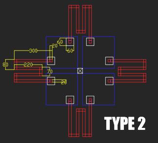
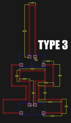
63 Common Piezoresistor Types
CMOS LAB MANUAL CMOS LAB MANUAL
 CMOS LAB MANUAL 2011 CMOS LAB MANUAL This manual was designed for use with the Montana Microfabrication Facility at MSU. The intention of the manual is to provide lab users and MSU students with a complete
Lab #2 Wafer Cleaning (RCA cleaning)
") Lab #2 Wafer Cleaning (RCA cleaning) RCA Cleaning System Used: Wet Bench 1, Bay1, Nanofabrication Center Chemicals Used: H 2 O : NH 4 OH : H 2 O 2 (5 : 1 : 1) H 2 O : HF (10 : 1) H 2 O : HCl : H 2 O 2
Lab #2 Wafer Cleaning (RCA cleaning) RCA Cleaning System Used: Wet Bench 1, Bay1, Nanofabrication Center Chemicals Used: H 2 O : NH 4 OH : H 2 O 2 (5 : 1 : 1) H 2 O : HF (10 : 1) H 2 O : HCl : H 2 O 2
Microelectronic Device Instructional Laboratory. Table of Contents
 Introduction Process Overview Microelectronic Device Instructional Laboratory Introduction Description Flowchart MOSFET Development Process Description Process Steps Cleaning Solvent Cleaning Photo Lithography
Report 1. B. Starting Wafer Specs Number: 10 Total, 6 Device and 4 Test wafers
 Aaron Pederson EE 432 Lab Dr. Meng Lu netid: abp250 Lab instructor: Yunfei Zhao Report 1 A. Overview The goal of this lab is to go through the semiconductor fabrication process from start to finish. This
EELE408 Photovoltaics Lecture 02: Silicon Processing
 EELE408 Photovoltaics Lecture 0: licon Processing Dr. Todd J. Kaiser tjkaiser@ece.montana.edu Department of Electrical and Computer Engineering Montana State University - Bozeman The Fabrication Process
Temperature Scales. Questions. Temperature Conversions 7/21/2010. EE580 Solar Cells Todd J. Kaiser. Thermally Activated Processes
 7/1/010 EE80 Solar Cells Todd J. Kaiser Flow of Wafer in Fabrication Lecture 0 Microfabrication A combination of Applied Chemistry, Physics and ptics Thermal Processes Diffusion & xidation Photolithograpy
EE 432/532 CyMOS process PWELL Lithography & Diffusion Feb 24, 2016
 EE 432/532 CyMOS process PWELL Lithography & Diffusion Feb 24, 2016 Friday Afternoon Group Brady Koht Sebastian Roe Peter Bonnie Joseph Wickner Lab Instructor Yunfei Zhao 1. Overview Now that a Field Oxide
PHYS 534 (Fall 2008) Process Integration OUTLINE. Examples of PROCESS FLOW SEQUENCES. >Surface-Micromachined Beam
 Process Integration OUTLINE. Examples of PROCESS FLOW SEQUENCES. >Surface-Micromachined Beam") PHYS 534 (Fall 2008) Process Integration Srikar Vengallatore, McGill University 1 OUTLINE Examples of PROCESS FLOW SEQUENCES >Semiconductor diode >Surface-Micromachined Beam Critical Issues in Process
PHYS 534 (Fall 2008) Process Integration Srikar Vengallatore, McGill University 1 OUTLINE Examples of PROCESS FLOW SEQUENCES >Semiconductor diode >Surface-Micromachined Beam Critical Issues in Process
Fabrication Technology
 Fabrication Technology By B.G.Balagangadhar Department of Electronics and Communication Ghousia College of Engineering, Ramanagaram 1 OUTLINE Introduction Why Silicon The purity of Silicon Czochralski
EE 432 CyMOS process PWELL Photolithography and Diffusion Feb. 23th 2017
 1 EE 432 CyMOS process PWELL Photolithography and Diffusion Feb. 23th 2017 Group III Jake Asmus (Leader) John Guss Shengliang Liu Xin Chen Lab instructor Matt Weinstein 2 Overview With the field oxide
Because of equipment availability, cost, and time, we will use aluminum as the top side conductor
 Because of equipment availability, cost, and time, we will use aluminum as the top side conductor Top Side Conductor vacuum deposition Aluminum sputter deposit in Argon plasma CVC 601-sputter deposition
3.155J / 6.152J Micro/Nano Processing Technology TAKE-HOME QUIZ FALL TERM 2005
 3.155J / 6.152J Micro/Nano Processing Technology TAKE-HOME QUIZ FALL TERM 2005 1) This is an open book, take-home quiz. You are not to consult with other class members or anyone else. You may discuss the
DEPARTMENT OF MECHANICAL SCIENCE AND ENGINEERING UNIVERSITY OF ILLINOIS. ME498 PV Class. Laboratory Manual on Fundamentals of Solar Cell Manufacturing
 DEPARTMENT OF MECHANICAL SCIENCE AND ENGINEERING UNIVERSITY OF ILLINOIS ME498 PV Class Laboratory Manual on Fundamentals of Solar Cell Manufacturing Prepared by Bruno Azeredo, and Dr. Elif Ertekin 9/21/2013
Thermal Oxidation and Growth of Insulators (Chapter 3 - Jaeger 3) Key advantage of Si: Oxidation of Si into SiO 2 (glass) Major factor in making
 Key advantage of Si: Oxidation of Si into SiO 2 (glass) Major factor in making") Thermal Oxidation and Growth of Insulators (Chapter 3 - Jaeger 3) Key advantage of Si: Oxidation of Si into SiO (glass) Major factor in making Silicon the main semiconductor Grown at high temperature in
Thermal Oxidation and Growth of Insulators (Chapter 3 - Jaeger 3) Key advantage of Si: Oxidation of Si into SiO (glass) Major factor in making Silicon the main semiconductor Grown at high temperature in
4. Thermal Oxidation. a) Equipment Atmospheric Furnace
 Equipment Atmospheric Furnace") 4. Thermal Oxidation a) Equipment Atmospheric Furnace Oxidation requires precise control of: temperature, T ambient gas, G time spent at any given T & G, t Vito Logiudice 34 4. Thermal Oxidation b) Mechanism
4. Thermal Oxidation a) Equipment Atmospheric Furnace Oxidation requires precise control of: temperature, T ambient gas, G time spent at any given T & G, t Vito Logiudice 34 4. Thermal Oxidation b) Mechanism
Surface micromachining and Process flow part 1
 Surface micromachining and Process flow part 1 Identify the basic steps of a generic surface micromachining process Identify the critical requirements needed to create a MEMS using surface micromachining
EE432/532 CYMOS PROCESS PWELL LITHOGRAPHY AND DIFFUSION
 EE432/532 CYMOS PROCESS PWELL LITHOGRAPHY AND DIFFUSION [Document subtitle] GROUP 4 GROUP 4 (TUESDAY AFTERNOON) GROUP LEADER: ANDREW MCNEIL GROUP MEMBERS: WENG HOONG LOO MARIO PEREZ ZHIHAO LIAO LAB INSTRUCTOR
Photolithography I ( Part 2 )
") 1 Photolithography I ( Part 2 ) Chapter 13 : Semiconductor Manufacturing Technology by M. Quirk & J. Serda Bjørn-Ove Fimland, Department of Electronics and Telecommunication, Norwegian University of Science
1 Photolithography I ( Part 2 ) Chapter 13 : Semiconductor Manufacturing Technology by M. Quirk & J. Serda Bjørn-Ove Fimland, Department of Electronics and Telecommunication, Norwegian University of Science
Module 1 and 2 Report
 Module 1 and 2 Report Interdisciplinary Microelectronics Processing Lab Group D Jaimie Stevens, Erich P. Meinig, Adam Longoria, Emily Makoutz, Ben Timmer Date: February 10, 2015 Abstract This report details
Fabrication Technology, Part I
 EEL5225: Principles of MEMS Transducers (Fall 2003) Fabrication Technology, Part I Agenda: Oxidation, layer deposition (last lecture) Lithography Pattern Transfer (etching) Impurity Doping Reading: Senturia,
Colorado School of Mines PHGN/CHGN 435. Modules 1 and 2. Authors: Garrick Johnson Trevor Haak Carl DuBois Ethan Palay
 Colorado School of Mines PHGN/CHGN 435 Modules 1 and 2 Authors: Garrick Johnson Trevor Haak Carl DuBois Ethan Palay February 10, 2015 1 Introduction and Background Integrated circuits are an integral part
Photolithography Process Technology
 Contents Photolithography Process - Wafer Preparation - Photoresist Coating - Align & Expose - Photoresist Development Process Control CD Measurement Equipment Expose System & Wafer Track Consumables Chemicals
Fabrication and Layout
 ECEN454 Digital Integrated Circuit Design Fabrication and Layout ECEN 454 3.1 A Glimpse at MOS Device Polysilicon Aluminum ECEN 475 4.2 1 Material Classification Insulators Glass, diamond, silicon oxide
ELEC 3908, Physical Electronics, Lecture 4. Basic Integrated Circuit Processing
 ELEC 3908, Physical Electronics, Lecture 4 Basic Integrated Circuit Processing Lecture Outline Details of the physical structure of devices will be very important in developing models for electrical behavior
EE 527 MICROFABRICATION. Lecture 15 Tai-Chang Chen University of Washington EE-527 M4 MASK SET: NPN BJT. C (sub) A E = 40 µm x 40 µm
 A E = 40 µm x 40 µm") EE 527 MICROFABRICATION Lecture 15 Tai-Chang Chen University of Washington EE-527 M4 MASK SET: NPN BJT C (sub) E B A E = 40 µm x 40 µm 1 EE-527 M4 MASK SET: MOS C-V TEST CAPACITORS W = 10 µm L = 10 µm
EE 527 MICROFABRICATION Lecture 15 Tai-Chang Chen University of Washington EE-527 M4 MASK SET: NPN BJT C (sub) E B A E = 40 µm x 40 µm 1 EE-527 M4 MASK SET: MOS C-V TEST CAPACITORS W = 10 µm L = 10 µm
Fabrication Process. Crystal Growth Doping Deposition Patterning Lithography Oxidation Ion Implementation CONCORDIA VLSI DESIGN LAB
 Fabrication Process Crystal Growth Doping Deposition Patterning Lithography Oxidation Ion Implementation 1 Fabrication- CMOS Process Starting Material Preparation 1. Produce Metallurgical Grade Silicon
Mostafa Soliman, Ph.D. May 5 th 2014
 Mostafa Soliman, Ph.D. May 5 th 2014 Mostafa Soliman, Ph.D. 1 Basic MEMS Processes Front-End Processes Back-End Processes 2 Mostafa Soliman, Ph.D. Wafers Deposition Lithography Etch Chips 1- Si Substrate
micro resist technology
 Characteristics Processing guidelines Negative Tone Photoresist Series ma-n 1400 ma-n 1400 is a negative tone photoresist series designed for the use in microelectronics and microsystems. The resists are
Selective-Area Atomic Layer Deposition (SA-ALD) of Titanium Dioxide (TiO 2) using Poly(methyl methacrylate) (PMMA) Michael Tu 5/12/2016
 of Titanium Dioxide (TiO 2) using Poly(methyl methacrylate) (PMMA) Michael Tu 5/12/2016") Selective-Area Atomic Layer Deposition (SA-ALD) of Titanium Dioxide (TiO 2) using Poly(methyl methacrylate) (PMMA) Michael Tu 5/12/2016 Introduction The Minnesota Nano Center s Keller Hall facility includes
Selective-Area Atomic Layer Deposition (SA-ALD) of Titanium Dioxide (TiO 2) using Poly(methyl methacrylate) (PMMA) Michael Tu 5/12/2016 Introduction The Minnesota Nano Center s Keller Hall facility includes
This Appendix discusses the main IC fabrication processes.
 IC Fabrication B B.1 Introduction This Appendix discusses the main IC fabrication processes. B.2 NMOS fabrication NMOS transistors are formed in a p-type substrate. The NMOS fabrication process requires
EE 5344 Introduction to MEMS. CHAPTER 3 Conventional Si Processing
 3. Conventional licon Processing Micromachining, Microfabrication. EE 5344 Introduction to MEMS CHAPTER 3 Conventional Processing Why silicon? Abundant, cheap, easy to process. licon planar Integrated
Process Flow in Cross Sections
 Process Flow in Cross Sections Process (simplified) 0. Clean wafer in nasty acids (HF, HNO 3, H 2 SO 4,...) --> wear gloves! 1. Grow 500 nm of SiO 2 (by putting the wafer in a furnace with O 2 2. Coat
How To Write A Flowchart
 1 Learning Objectives To learn how you transfer a device concept into a process flow to fabricate the device in the EKL labs You learn the different components that makes up a flowchart; process blocks,
3.155J / 6.152J MICROELECTRONICS PROCESSING TECHNOLOGY TAKE-HOME QUIZ FALL TERM 2003
 3.155J / 6.152J MICROELECTRONICS PROCESSING TECHNOLOGY TAKE-HOME QUIZ FALL TERM 2003 1) This is an open book, take-home quiz. You are not to consult with other class members or anyone else. You may discuss
Lab 1: Field Oxide. Overview. Starting Wafers
 Overview Lab 1: Field Oxide Brandon Baxter, Robert Buckley, Tara Mina, Quentin Vingerhoets Lab instructor: Liang Zhang Course Instructor: Dr. Gary Tuttle EE 432-532 January 23, 2017 In this lab we created
Czochralski Crystal Growth
 Czochralski Crystal Growth Crystal Pulling Crystal Ingots Shaping and Polishing 300 mm wafer 1 2 Advantage of larger diameter wafers Wafer area larger Chip area larger 3 4 Large-Diameter Wafer Handling
EE 330 Lecture 8. IC Fabrication Technology Part II. - Oxidation - Epitaxy - Polysilicon - Interconnects
 EE 330 Lecture 8 IC Fabrication Technology Part II - Oxidation - Epitaxy - Polysilicon - Interconnects Review from Last Time MOS Transistor Bulk Source Gate Drain p-channel MOSFET Lightly-doped n-type
Bulk MEMS Fabrication Details Dr. Lynn Fuller, Casey Gonta, Patsy Cadareanu
 ROCHESTER INSTITUTE OF TECHNOLOGY MICROELECTRONIC ENGINEERING Bulk MEMS Fabrication Details Dr. Lynn Fuller, Casey Gonta, Patsy Cadareanu Webpage: http://people.rit.edu/lffeee 82 Lomb Memorial Drive Rochester,
All fabrication was performed on Si wafers with 285 nm of thermally grown oxide to
 Supporting Information: Substrate preparation and SLG growth: All fabrication was performed on Si wafers with 285 nm of thermally grown oxide to aid in visual inspection of the graphene samples. Prior
Total Points = 110 possible (graded out of 100)
") Lab Report 1 Table of Contents 1. Profiles & Layout (9 Points) 2. Process Procedures (20 points) 3. Calculations (36 Points) 4. Questions (35 Points) 5. Bonus Questions (10 Points) Total Points = 110 possible
Lab Report 1 Table of Contents 1. Profiles & Layout (9 Points) 2. Process Procedures (20 points) 3. Calculations (36 Points) 4. Questions (35 Points) 5. Bonus Questions (10 Points) Total Points = 110 possible
MEMS Surface Fabrication
 ROCHESTER INSTITUTE OF TECHNOLOGY MICROELECTRONIC ENGINEERING MEMS Surface Fabrication Dr. Lynn Fuller webpage: http://people.rit.edu/lffeee Electrical and Microelectronic Engineering Rochester Institute
Be careful what you wish for
 Be careful what you wish for Four Point Probe Key measurement tool in microelectronics fabrication What is Four Point Probing Four Point Probing is a method for measuring the resistivity of a substance.
Chapter 2 Manufacturing Process
 Digital Integrated Circuits A Design Perspective Chapter 2 Manufacturing Process 1 CMOS Process 2 CMOS Process (n-well) Both NMOS and PMOS must be built in the same silicon material. PMOS in n-well NMOS
Wireless implantable chip with integrated Nitinol-based pump for radio-controlled local drug delivery
 Electronic Supplementary Material (ESI) for Lab on a Chip. This journal is The Royal Society of Chemistry 2014 Electronic Supplementary Information Wireless implantable chip with integrated Nitinol-based
User Fees for the 4D LABS Fabrication Facility
 User Fees for the 4D LABS Fabrication Facility 1. Clean Room Fees Service Clean Room access: Includes use of all Clean Room tools except for those in the groups listed below Group I tools: Plasma reactors
Buffered Oxide Etch STANDARD OPERATING PROCEDURE
 Buffered Oxide Etch STANDARD OPERATING PROCEDURE TABLE OF CONTENTS: 1. SUMMARY..2 2. INTRODUCTION...3 3. LOCATION OF EQUIPMENT, ACCESSORIES, TOOLS AND SUPPLIES.4 4. PERSONAL SAFETY EQUIPMENT...5 5. MATERIAL
The Physical Structure (NMOS)
") The Physical Structure (NMOS) Al SiO2 Field Oxide Gate oxide S n+ Polysilicon Gate Al SiO2 SiO2 D n+ L channel P Substrate Field Oxide contact Metal (S) n+ (G) L W n+ (D) Poly 1 3D Perspective 2 3 Fabrication
The Physical Structure (NMOS) Al SiO2 Field Oxide Gate oxide S n+ Polysilicon Gate Al SiO2 SiO2 D n+ L channel P Substrate Field Oxide contact Metal (S) n+ (G) L W n+ (D) Poly 1 3D Perspective 2 3 Fabrication
Dow Corning WL-5150 Photodefinable Spin-On Silicone
 Dow Corning WL-515 Photodefinable Spin-On Silicone Properties and Processing Procedures Introduction Dow Corning WL-515 is a silicone formulation which can be photopatterned and cured using standard microelectronics
Chapter 2 MOS Fabrication Technology
 Chapter 2 MOS Fabrication Technology Abstract This chapter is concerned with the fabrication of metal oxide semiconductor (MOS) technology. Various processes such as wafer fabrication, oxidation, mask
Low-temperature, Simple and Fast Integration Technique of Microfluidic Chips by using a UV-curable Adhesive
 Low-temperature, Simple and Fast Integration Technique of Microfluidic Chips by using a UV-curable Adhesive Supplementary Information Channel fabrication Glass microchannels. A borosilicate glass wafer
Lab 2: PWELL Lithography and Diffusion
 Brandon Baxter, Robert Buckley Lab Instructor: Liang Zhang Course Instructor: Gary Tuttle EE 432-532 Due: February 23, 2017 Lab 2: PWELL Lithography and Diffusion 1. Overview The purpose of this lab was
GLM General information. Technical Datasheet
 GLM 2060 Nanocomposite SU-8-negative tone photo-epoxy for layers from 6.0 to 50µm Technical Datasheet Gersteltec Sarl. Générale Guisan 26, 1009, Pully Switzerland Switzerland / Israel / Taiwan Contact:
Thomas M. Adams Richard A. Layton. Introductory MEMS. Fabrication and Applications. Springer
 Thomas M. Adams Richard A. Layton Introductory MEMS Fabrication and Applications Springer Contents Preface xiü Part I Fabrication Chapter 1: Introduction 3 1.1 What are MEMS? 3 1.2 Why MEMS? 4 1.2.1. Low
Chapter 3 CMOS processing technology
 Chapter 3 CMOS processing technology (How to make a CMOS?) Si + impurity acceptors(p-type) donors (n-type) p-type + n-type => pn junction (I-V) 3.1.1 (Wafer) Wafer = A disk of silicon (0.25 mm - 1 mm thick),
EECS130 Integrated Circuit Devices
 EECS130 Integrated Circuit Devices Professor Ali Javey 9/13/2007 Fabrication Technology Lecture 1 Silicon Device Fabrication Technology Over 10 15 transistors (or 100,000 for every person in the world)
Processing guidelines. Negative Tone Photoresists mr-ebl 6000
 Characteristics Processing guidelines Negative Tone Photoresists mr-ebl 6000 mr-ebl 6000 is a chemically amplified negative tone photoresist for the use in micro- and nanoelectronics. - Electron beam sensitive
Diffusion/Anneal SOP Page 1 of 12 Revision
 Diffusion/Anneal SOP Diffusion/Anneal SOP Page 1 of 12 1 Scope 1.1 This document provides the procedures and requirements to introduce and/or drive dopants into silicon using the Canary furnace. 2 Table
EE 457 : Multilayer Devices
 March 1, 2010 EE 457 : Multilayer Devices by prepared for: Prof. K. Westra M. Mohammed EE 457: Multilayer Devices Objectives...1 Process Flow...1 1.Cleaning...1 2.Thermal Oxidation...1 3.Aluminum Sputtering...1
EE 330 Lecture 9. IC Fabrication Technology Part II. -Oxidation -Epitaxy -Polysilicon -Planarization -Resistance and Capacitance in Interconnects
 EE 330 Lecture 9 IC Fabrication Technology Part II -Oxidation -Epitaxy -Polysilicon -Planarization -Resistance and Capacitance in Interconnects Review from Last Time IC Fabrication Technology Crystal Preparation
Lecture 19 Microfabrication 4/1/03 Prof. Andy Neureuther
 EECS 40 Spring 2003 Lecture 19 Microfabrication 4/1/03 Prof. ndy Neureuther How are Integrated Circuits made? Silicon wafers Oxide formation by growth or deposition Other films Pattern transfer by lithography
2015 EE410-LOCOS 0.5µm Poly CMOS Process Run Card Lot ID:
 STEP 0.00 - PHOTOMASK #0- ZERO LEVEL MARKS Starting materials is n-type silicon (5-10 ohm-cm). Add four test wafers labeled T1-T4. T1 and T2 will travel with the device wafers and get all of the processing
CS/ECE 5710/6710. N-type Transistor. N-type from the top. Diffusion Mask. Polysilicon Mask. CMOS Processing
 CS/ECE 5710/6710 CMOS Processing Addison-Wesley N-type Transistor D G +Vgs + Vds S N-type from the top i electrons - Diffusion Mask Mask for just the diffused regions Top view shows patterns that make
ECE 440 Lecture 27 : Equilibrium P-N Junctions I Class Outline:
 ECE 440 Lecture 27 : Equilibrium P-N Junctions I Class Outline: Fabrication of p-n junctions Contact Potential Things you should know when you leave Key Questions What are the necessary steps to fabricate
Photoresist Coat, Expose and Develop Laboratory Dr. Lynn Fuller
 ROCHESTER INSTITUTE OF TECHNOLOGY MICROELECTRONIC ENGINEERING Photoresist Coat, Expose and Develop Laboratory Dr. Lynn Fuller Webpage: http://www.rit.edu/lffeee 82 Lomb Memorial Drive Rochester, NY 14623-5604
Silicon Manufacturing
 Silicon Manufacturing Group Members Young Soon Song Nghia Nguyen Kei Wong Eyad Fanous Hanna Kim Steven Hsu th Fundamental Processing Steps 1.Silicon Manufacturing a) Czochralski method. b) Wafer Manufacturing
micro resist technology
 Characteristics Processing guidelines Negative Tone Photoresist Series ma-n 2400 ma-n 2400 is a negative tone photoresist series designed for the use in micro- and nanoelectronics. The resists are available
Complexity of IC Metallization. Early 21 st Century IC Technology
 EECS 42 Introduction to Digital Electronics Lecture # 25 Microfabrication Handout of This Lecture. Today: how are Integrated Circuits made? Silicon wafers Oxide formation by growth or deposition Other
Etching Etching Definitions Isotropic Etching: same in all direction Anisotropic Etching: direction sensitive Selectivity: etch rate difference
 Etching Etching Definitions Isotropic Etching: same in all direction Anisotropic Etching: direction sensitive Selectivity: etch rate difference between 2 materials Need strong selectivity from masking
CyMOS process Spring 2016 Iowa State University
 CyMOS process Spring 2016 Iowa State University Start Date Starting Material Orientation: Dopant: Resistivity: Ω cm Doping Concentration: cm 3 Diameter: inch Thickness: µm Lot Identification: Wafer Count
EE 330 Lecture 8. IC Fabrication Technology Part II. - Masking - Photolithography - Deposition - Etching - Diffusion
 EE 330 Lecture 8 IC Fabrication Technology Part II?? - Masking - Photolithography - Deposition - Etching - Diffusion Review from Last Time Technology Files Provide Information About Process Process Flow
Semiconductor device fabrication
 REVIEW Semiconductor device fabrication is the process used to create the integrated circuits (silicon chips) that are present in everyday electrical and electronic devices. It is a multiplestep sequence
Microfabrication of Integrated Circuits
 Microfabrication of Integrated Circuits OUTLINE History Basic Processes Implant; Oxidation; Photolithography; Masks Layout and Process Flow Device Cross Section Evolution Lecture 38, 12/05/05 Reading This
Development of Silicon Pad and Strip Detector in High Energy Physics
 XXI DAE-BRNS High Energy Physics Symposium 2014, IIT Guwahati Development of Silicon Pad and Strip Detector in High Energy Physics Manoj Jadhav Department of Physics I.I.T. Bombay 2 Manoj Jadhav, IIT Bombay.
A discussion of crystal growth, lithography, etching, doping, and device structures is presented in
 Chapter 5 PROCESSING OF DEVICES A discussion of crystal growth, lithography, etching, doping, and device structures is presented in the following overview gures. SEMICONDUCTOR DEVICE PROCESSING: AN OVERVIEW
Chapter 3 Silicon Device Fabrication Technology
 Chapter 3 Silicon Device Fabrication Technology Over 10 15 transistors (or 100,000 for every person in the world) are manufactured every year. VLSI (Very Large Scale Integration) ULSI (Ultra Large Scale
Supporting Information: Model Based Design of a Microfluidic. Mixer Driven by Induced Charge Electroosmosis
 Supporting Information: Model Based Design of a Microfluidic Mixer Driven by Induced Charge Electroosmosis Cindy K. Harnett, Yehya M. Senousy, Katherine A. Dunphy-Guzman #, Jeremy Templeton * and Michael
EE 330 Lecture 9. IC Fabrication Technology Part 2
 EE 330 Lecture 9 IC Fabrication Technology Part 2 Quiz 8 A 2m silicon crystal is cut into wafers using a wire saw. If the wire diameter is 220um and the wafer thickness is 350um, how many wafers will this
Major Fabrication Steps in MOS Process Flow
 Major Fabrication Steps in MOS Process Flow UV light Mask oxygen Silicon dioxide photoresist exposed photoresist oxide Silicon substrate Oxidation (Field oxide) Photoresist Coating Mask-Wafer Alignment
Electronics Design Center Equipment
 Equipment The contains a variety of equipment used in the production, packaging and testing of microfabricated devices. The major equipment is located in one of three labs, the Room 21 fabrication laboratory,
EE 143 MICROFABRICATION TECHNOLOGY FALL 2014 C. Nguyen PROBLEM SET #9
 Issued: Tuesday, Nov. 11, 2014 PROBLEM SET #9 Due: Wednesday, Nov. 19, 2010, 8:00 a.m. in the EE 143 homework box near 140 Cory 1. The following pages comprise an actual pwell CMOS process flow with poly-to-poly
Graphene Biotransistor Interfaced with a Nitrifying Biofilm
 Supporting Information Graphene Biotransistor Interfaced with a Nitrifying Biofilm Morgan Brown 1, Leila Barker 2, Lewis Semprini 2 and Ethan D. Minot 1 1 Department of Physics, Oregon State University
Mikrosensorer. Microfabrication 1
 Mikrosensorer Microfabrication 1 Literature Introductory MEMS Fabrication and Applications Thomas M. Adams and Richard A. Layton Available as ebook on http://www.lub.lu.se/en/search/lubsearch.html This
SU-8 Overhanging Structures Using a Photoresist Sacrificial Layer and Embedded Aluminum Mask
 SU-8 Overhanging Structures Using a Photoresist Sacrificial Layer and Embedded Aluminum Mask By: See-Ho Tsang, Dan Sameoto, Sae-Won Lee A MAJOR PROJECT REPORT SUBMITTED IN PARTIAL FULLFILLMENT FOR ENGINEERING
The following are the completed but unbalanced equations. Each equation is numbered to match each step of the cycle:
 REACTIONS OF COPPER Copper will undergo many types of reactions. In this experiment you will observe a sequence of copper reactions. The sequence begins with copper metal and ends with copper metal, so
PROCESS FLOW AN INSIGHT INTO CMOS FABRICATION PROCESS
 Contents: VI Sem ECE 06EC63: Analog and Mixed Mode VLSI Design PROCESS FLOW AN INSIGHT INTO CMOS FABRICATION PROCESS 1. Introduction 2. CMOS Fabrication 3. Simplified View of Fabrication Process 3.1 Alternative
COPPER CYCLE EXPERIMENT 3
 COPPER CYCLE EXPERIMENT 3 INTRODUCTION One simple way to state the aim of chemistry is: The study of matter and its transformations. In this experiment, a copper sample will appear in five different forms
Nanoelectronics Fabrication Facility
 Nanoelectronics Fabrication Facility Contents Introduction 2 Mask Making Module 4 Photolithography Module 6 Wet Etching and CMP Module 8 Dry Etching and Sputtering Module 10 Thermal Process and Implantation
Semiconductor Device Fabrication Study
 Proceedings of The National Conference on Undergraduate Research (NCUR) 2003 University of Utah, Salt Lake City, Utah March 13-15, 2003 Semiconductor Device Fabrication Study Tsung-Ta Ho and Michael R.
There are basically two approaches for bulk micromachining of. silicon, wet and dry. Wet bulk micromachining is usually carried out
 57 Chapter 3 Fabrication of Accelerometer 3.1 Introduction There are basically two approaches for bulk micromachining of silicon, wet and dry. Wet bulk micromachining is usually carried out using anisotropic
Nitride Deposition SOP Page 1 of 14 Revision
 Nitride Deposition SOP Nitride Deposition SOP Page 1 of 14 1 Scope 1.1 This document provides the procedures and requirements to deposit silicon nitride films, using the Canary LPCVD furnace. 2 Table of
Design and Fabrication of a Micromechanical Pressure Sensor
 Design and Fabrication of a Micromechanical Pressure Sensor Neal V. Lafferty Microelectronic Engineering Rochester Institute of Technology Rochester, NY 14623 Abstract A Microelectromechanical (MEMS) pressure
Processing guidelines. Negative Tone Photoresist Series ma-n 2400
 Characteristics Processing guidelines Negative Tone Photoresist Series ma-n 2400 ma-n 2400 is a negative tone photoresist series designed for the use in micro- and nanoelectronics. The resists are available
Basic&Laboratory& Materials&Science&and&Engineering& Micro&Electromechanical&Systems&& (MEMS)&
&") Basic&Laboratory& Materials&Science&and&Engineering& Micro&Electromechanical&Systems&& (MEMS)& M105& As of: 27.10.2011 1 Introduction... 2 2 Materials used in MEMS fabrication... 2 3 MEMS fabrication processes...
Basic&Laboratory& Materials&Science&and&Engineering& Micro&Electromechanical&Systems&& (MEMS)& M105& As of: 27.10.2011 1 Introduction... 2 2 Materials used in MEMS fabrication... 2 3 MEMS fabrication processes...
Lecture 22: Integrated circuit fabrication
 Lecture 22: Integrated circuit fabrication Contents 1 Introduction 1 2 Layering 4 3 Patterning 7 4 Doping 8 4.1 Thermal diffusion......................... 10 4.2 Ion implantation.........................
Lecture 5: Micromachining
 MEMS: Fabrication Lecture 5: Micromachining Prasanna S. Gandhi Assistant Professor, Department of Mechanical Engineering, Indian Institute of Technology, Bombay, Recap: Last Class E-beam lithography X-ray
IC/MEMS Fabrication - Outline. Fabrication
 IC/MEMS Fabrication - Outline Fabrication overview Materials Wafer fabrication The Cycle: Deposition Lithography Etching Fabrication IC Fabrication Deposition Spin Casting PVD physical vapor deposition
Semiconductor Technology
 Semiconductor Technology from A to Z Oxidation www.halbleiter.org Contents Contents List of Figures List of Tables II III 1 Oxidation 1 1.1 Overview..................................... 1 1.1.1 Application...............................
MCC. LOR Lift-Off Resists LOR RESISTS OFFER TYPES OF RESISTS
 MCC LOR RESISTS OFFER Submicron linewidth control Finely tuned undercuts Does not intermix with imaging resists (no scum) Excellent adhesion to Si, NiFe, GaAs, InP and many other III-V and II-VI materials
UV15: For Fabrication of Polymer Optical Waveguides
 CASE STUDY UV15: For Fabrication of Polymer Optical Waveguides Master Bond Inc. 154 Hobart Street, Hackensack, NJ 07601 USA Phone +1.201.343.8983 Fax +1.201.343.2132 main@masterbond.com CASE STUDY UV15:
CYCLOTENE* 4000 Series Advanced Electronic Resins (Photo BCB)
") Revised: February 2005 CYCLOTENE* 4000 Series Advanced Electronic Resins (Photo BCB) Processing Procedures for CYCLOTENE 4000 Series Photo BCB Resins DS2100 Puddle Develop Process 1. Introduction The CYCLOTENE
Revised: February 2005 CYCLOTENE* 4000 Series Advanced Electronic Resins (Photo BCB) Processing Procedures for CYCLOTENE 4000 Series Photo BCB Resins DS2100 Puddle Develop Process 1. Introduction The CYCLOTENE