EV Group 300mm Wafer Bonding Technology July 16, 2008
|
|
|
- Lee Brown
- 6 years ago
- Views:
Transcription
1 EV Group 300mm Wafer Bonding Technology July 16, 2008

2 EV Group in a Nutshell st Our philosophy Our mission in serving next generation application in semiconductor technology Equipment supplier for the semiconductor and MEMS industry equipment installations Privately held company founded in 1980 Headquartered in Austria - subsidiaries in USA, JP, KR and TW Worldwide Sales and Customer Support Network Internal process development (2000m 2 class 100 cleanroom) 20% of revenue is invested into R&D annually


3 EVG core competences GEMINI IQ Aligner NanoSpray Coater DUV Exposure Courtesy of CEETAM TSV: Coating of highaspect ratio vias with dielectrics or photoresists
4 Innovations in Wafer Bonding 1990 First EVG Wafer Bonder with Process Separation Align - Bond First 150mm Bonding System with top and bottom side heating First Bonder with 40kN Piston Force First 200mm Bonding System; Introduction of SmartView Technology 2000 Double-side water cooling; First UV Bond System with optical alignment 2002 First 300mm Bonding System 2003 First system for LowTemp plasma activation 2003 First Chip-to-Wafer System with controllable center of gravity 2005 Second generation (IS) double-sided water cooling system 2005 First Bonder with 60kN Piston Force 2008 First 300mm production bonding system Third generation 100kN double-sided water cooling system SmartView NT Aligner


5 Wafer bonding for 3D integration Cu/Cu SOLID process Top wafer Courtesy of Courtesy of INFINEON Technologies Cu/BCB Via-First BCB BCB SiO2 Cu Fusion bonding 1 µm SiO2 Courtesy of Si LowTemp plasma activation

6 Wafer Bonding Process Separation Principle

7 SmartView Aligner Face-to-face wafer alignment with alignment keys in bond interface Patented Technology Integration with production wafer bonding system GEMINI Product development history 1 st 200mm Systems installed in Field st 300mm Systems installed in Field st GEMINI production bonder st GEMINI with Cleaner st GEMINI with LowTemp Plasma Activation st GEMINI for Transparent Packaging st GEMINI contained in N2 environment 2006
8 SmartView Aligner Working Principle To p Side Objective Bottom Wafer Alignment in contact plane Locate bottom wafer alignment marks with top objectives Lock microscope position Store bottom wafer position Top Wafer Bottom Side Objective Align top wafer to bottom objectives No microscope movement No re-focussing Positioning System Bring wafers in contact Restore bottom wafer position Contact plane = alignment focal plane No blind movement
9 Analysis of contributions to alignment error 1. Translational misalignment 2. Rotational misalignment 3. Run-out Thermal expansion mismatch between top and bottom wafer
10 Post bond metrology Electrical vernier structures generate alignment vector plots NPCQ2B4785 wafer B SEE1 tested , 3 Statistical process control Shift Rotation Run-out 2, , , 2 1, 2 1, 2 1, 2 RMS misalignment 3.2 um Average offset code 0.4, 2. 90% valid 81% X valid 100% Y valid 1, 2 1, 2 1, 2 1, 2 Greyed arrows and values of 99 or -99 indicate that one or both tests gave invalid results at that position. A grey arrow is drawn if one test was valid and so incomplete direction Analysis of impacting factors Bond process parameters 2, 1 2, 0 2, -2 2, -3 1, -4 information is available. A grey open circle is drawn if both tests were invalid and no direction information is available. NPCQ1A4613 wafer B SEH2 tested Bond layer (Reflowing material, surface properties,..) 0, 1 0, 1 0, -1 0, -2 0, -3 1, , RMS misalignment Technical implementation GEM300, SECS II/GEM Wafer ID Bondtool ID Bondchamber ID,.. -1, 1-2, 1-3, 1-1, 0-2, 0-4, 0-4, 0-5, 0-1, 0-2, -1-3, -1-4, -1-5, -1-1, -2-2, , -2-4, -3-5, -4 0, -3-2, -3-3, -3-4, -4-5, -4 0, -4-2, -4-3, -4-4, -4-1, -6-2, -6-3, um Average offset code -1.7, % valid 98% X valid 95% Y valid Greyed arrows and values of 99 or -99 indicate that one or both tests gave invalid results at that position. A grey arrow is drawn if one test was valid and so incomplete direction information is available. A grey open circle is drawn if both tests were invalid and no direction information is available.
11 Bonding Methods / Alignment Capability Alignment System Capability Alignment Method Alignment Accuracy at 3 Sigma Transparent Wafer +/- 0,5 µm Backside Alignment +/- 2µm SmartView Face-to-Face Alignment +/- 1,3 µm Post Bond Alignment Accuracy - Add to Alignment System Capability Bonding Technology Remark Alignment Accuracy at 3 Sigma Anodic Bonding Optimum Contrast Metalized Alignment Key, 4" Wafer, CTE +/- 1µm matched bond glass Glass Fritt Bonding ** 10µm screen printed glass fritt, Ferro , compressed to 4-6µm during bonding process, 150mm or 200mm +/- 5µm Wafer Polymer Thermo Compression Bond Thin spin coated adhesive (<1µm), 150 or 200mm Si-wafer +/- 0,6µm Fusion Bonds (Si + Si, SiO2+SiO 2 ) +/- 0,4 µm Metal Intermediate Layer Thermo Compression Bond Thin (<2µm) metal layer to form an eutectic bond or metal to metal fusion bond. (such as: Au-Si, Cu-Cu...) +/- 0,6µm ** Also applicable to other thick (>5µm) and reflowing intermediate layers.
 EVG")
12 Roadmap for post-bond alignment accuracy ITRS Roadmap ITRS 2007 High Density Through Silicon via Draft Specification ( ) EVG Roadmap

13 Design of SmartView NT

14 SmartView - NT (Nano Align Technology) Next Technology Generation New Basic Set-up High stiffness and perfect surface preparation New base frame (welded) New additional Nano Alignment Stage Nano steps do- and controllable Compensate misalignments during z-movements New Measurement Systems Laser System Permanent control of movement during alignment No blind movement anymore Continuous improvement program over 5 years
15 Optical System Improvements for ITRS roadmap 1. Optics: Improved microscopes Image quality, resolution, stability 2. In-situ optic calibration Alignment accuracy independent from mechanical setup 3. Pattern recognition: based on synthetic patterns Alignment accuracy independent from pattern variation 4. Signal processing: Digital cameras No disturbances from environment, higher signal-to-noise 5. Statistical Process Control: GEM300, SECS II/GEM

16 Precision Alignment Stage High precision alignment Stage allows movement in X, Y and φ direction Technical Data X: ± 13 µm Y: ± 13 µm Φ: ± 0.08 Min. controllable step: 8 nm Compensate misalignment due to kneeling of tables and/or during movements in Z direction Integrated Measurement System with highest Resolution (nm)

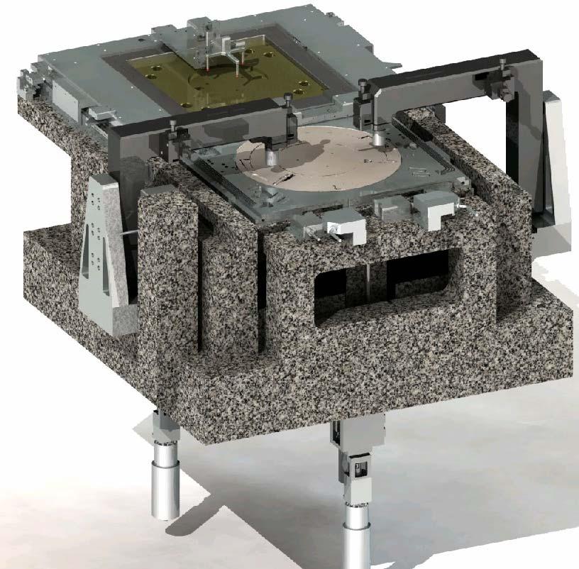
17 300mm production wafer bonding systems EVG560 Up to 4 bond chambers Center-to-center wafer alignment Cassette-to-cassette operation EVG Gemini Combines the EVG560 with the SmartView aligner Optical alignment Integration of pre-processes for wafer bonding Cleaning Plasma activation Adhesive coating

 Alignment accuracy Throughput Ziptronix Direct Bond")
18 Wafer bonding for 3D integration Bonding methods Fusion bonding Thermocompression bonding Metal-metal Dielectric bonding e.g. BCB Hybrid methods Fusion + Cu BCB + Cu Decision criteria Integration scheme Surface properties (flatness, roughness) Alignment accuracy Throughput Ziptronix Direct Bond Interconnect (DBI ), Courtesy of Ziptronix Metal/Adhesive 3D Bonding; Courtesy of RPI


19 Bonding methods for 3D integration Room Temperature pre-bond Fusion bonding Highest alignment accuracy No thermal expansion mismatch Highest throughput Batch annealing Tough surface specs High temperature bonds Thermocompression bonding Easier manufacturing schemes Moderate surface specs Pixel Cross-Section of Functional 3D-integrated, 3-tier APD Focal Plane; Courtesy of MIT Lincoln Laboratory, presented at 2006 ISSCC. CMOS SOI BCB Si Courtesy of Freescale Source: P. Morrow et. al, IEEE Electron Device Letters, Vol. 27, No. 5, May 2006, pp335

20 Comparision 3D Bonding Processes SmartView Aligned Cu-Cu BCB SiO 2 Most Promising Roadmap
21 Comparision 3D Bonding Processes SmartView Aligned SiO 2 bonds are ~35% more accurate today, have best potential for further improvement and provide a 10x faster process. SiO 2
22 LowTemp Plasma Bonding for 3D Integration Fusion wafer bonding is a 2-step process 1. Room temperature pre-bond 2. High temperature annealing Traditional fusion bonding methods require annealing temperatures of C. LowTemp plasma activation enables reduction of annealing temperature down to C. Fusion wafer bonding is ideally suited for 3D integration. Pre-bonding at room temperature enables highest alignment accuracy Bond quality inspection prior to annealing rework possible Low manufacturing costs due to batch annealing Metal ion and particle free bonding Si/CMOS 200mm wafers bonded with plasma activated wafer bonding and annealed at 300 C.


23 GEMINI the modular production platform Plasma Chamber SmartView Aligner EVG560 with 4 Bond Chambers Integration of cleaning chamber LowTemp plasma activation SMIF / FOUP Interface GEMINI for transparent packaging: Coating of adhesives UV bond module Wafer-to-Wafer Bonding
24 Summary EVG SmartView NT Newest generation of wafer bond aligner Highest flexibility for substrate properties Established alignment principle, but new design Roadmap 2009: Oxide bond (300mm) 0.3µm (3σ) Cu-Cu Bond (300mm) 0.9µm (3σ) EVG Gemini Cassette-to-cassette production wafer bonding system Integration of pre-bond process modules Plasma activation Wafer cleaning Supports all bonding methods and materials Polymer based thermo compression bonding Metal thermocompression bonding Oxide bonding


25 Questions? For further discussions please do not hesitate to contact me. Thorsten Matthias Director of Technology, EVG North America Tel.: Semicon West 2008 Booth 5429 North Hall
26 EV Group
Trends in Device Encapsulation and Wafer Bonding
 Trends in Device Encapsulation and Wafer Bonding Roland Weinhäupl, Sales Manager, EV Group Outline Introduction Vacuum Encapsulation Metal Bonding Overview Conclusion Quick Introduction to EV Group st
TSV Processing and Wafer Stacking. Kathy Cook and Maggie Zoberbier, 3D Business Development
 TSV Processing and Wafer Stacking Kathy Cook and Maggie Zoberbier, 3D Business Development Outline Why 3D Integration? TSV Process Variations Lithography Process Results Stacking Technology Wafer Bonding
Thin Wafers Bonding & Processing
 Thin Wafers Bonding & Processing A market perspective 2012 Why New Handling Technologies Consumer electronics is today a big driver for smaller, higher performing & lower cost device configurations. These
NOVEL BONDING TECHNOLOGIES FOR WAFER-LEVEL TRANSPARENT PACKAGING OF MOEMS. Herwig Kirchberger, Paul Lindner, Markus Wimplinger
 Stresa, Italy, 25-27 April 2007 NOVEL BONDING TECHNOLOGIES FOR WAFER-LEVEL TRANSPARENT PACKAGING OF MOEMS Herwig Kirchberger, Paul Lindner, Markus Wimplinger EV Group, A-4782 St. Florian, DI Erich Thallner
Metal bonding. Aida Khayyami, Kirill Isakov, Maria Grigoreva Miika Soikkeli, Sample Inkinen
 Metal bonding Aida Khayyami, Kirill Isakov, Maria Grigoreva Miika Soikkeli, Sample Inkinen Timing (delete before presentation) Introduction (Outline, available bonding techniques, evaluation of metal bondings)-3
Fraunhofer ENAS Current results and future approaches in Wafer-level-packaging FRANK ROSCHER
 Fraunhofer ENAS - Current results and future approaches in Wafer-level-packaging FRANK ROSCHER Fraunhofer ENAS Chemnitz System Packaging Page 1 System Packaging Outline: Wafer level packaging for MEMS
3D-IC Integration using D2C or D2W Alignment Schemes together with Local Oxide Reduction
 3D-IC Integration using D2C or D2W Alignment Schemes together with Local Oxide Reduction Gilbert Lecarpentier*, Jean-Stéphane Mottet* SET S.A.S. (Smart Equipment Technology), 131 Impasse Barteudet, 74490
Czochralski Crystal Growth
 Czochralski Crystal Growth Crystal Pulling Crystal Ingots Shaping and Polishing 300 mm wafer 1 2 Advantage of larger diameter wafers Wafer area larger Chip area larger 3 4 Large-Diameter Wafer Handling
BONDING OF MULTIPLE WAFERS FOR HIGH THROUGHPUT LED PRODUCTION. S. Sood and A. Wong
 10.1149/1.2982882 The Electrochemical Society BONDING OF MULTIPLE WAFERS FOR HIGH THROUGHPUT LED PRODUCTION S. Sood and A. Wong Wafer Bonder Division, SUSS MicroTec Inc., 228 SUSS Drive, Waterbury Center,
AML. AML- Technical Benefits. 4 Sept Wafer Bonding Machines & Services MEMS, IC, III-Vs.
 AML AML- Technical Benefits 4 Sept 2012 www.aml.co.uk AML In-situ Aligner Wafer Bonders Wafer bonding capabilities:- Anodic Bonding Si-Glass Direct Bonding e.g. Si-Si Glass Frit Bonding Eutectic Bonding
PHYS 534 (Fall 2008) Process Integration OUTLINE. Examples of PROCESS FLOW SEQUENCES. >Surface-Micromachined Beam
 Process Integration OUTLINE. Examples of PROCESS FLOW SEQUENCES. >Surface-Micromachined Beam") PHYS 534 (Fall 2008) Process Integration Srikar Vengallatore, McGill University 1 OUTLINE Examples of PROCESS FLOW SEQUENCES >Semiconductor diode >Surface-Micromachined Beam Critical Issues in Process
PHYS 534 (Fall 2008) Process Integration Srikar Vengallatore, McGill University 1 OUTLINE Examples of PROCESS FLOW SEQUENCES >Semiconductor diode >Surface-Micromachined Beam Critical Issues in Process
Lecture 5. SOI Micromachining. SOI MUMPs. SOI Micromachining. Silicon-on-Insulator Microstructures. Agenda:
 EEL6935 Advanced MEMS (Spring 2005) Instructor: Dr. Huikai Xie SOI Micromachining Agenda: SOI Micromachining SOI MUMPs Multi-level structures Lecture 5 Silicon-on-Insulator Microstructures Single-crystal
Laser Micromachining for Industrial Applications and R&D. 3D-Micromac AG. Symposium on Smart Integrated Systems in Chemnitz. 3D-Micromac AG
 3D-Micromac AG Symposium on Smart Integrated Systems in Chemnitz 1 1 microdice - TLS-Dicing for separation of SiC 2 microprep - for high-throughput microstructure diagnostics 3 About 3D-Micromac AG 2 microdice
SUSS MICROTEC - SEMI MEMS TECH SEMINAR Mailand, 23. September Margarete Zoberbier, Product Manager Bonder
 SUSS MICROTEC - SEMI MEMS TECH SEMINAR Mailand, 23. September 2014 Margarete Zoberbier, Product Manager Bonder SUSS MICROTEC AT A GLANCE Facts 60+ years of experience in semiconductor equipment Two facilities
CERN/NA62 GigaTracKer Hybrid Module Manufacturing
 CERN/NA62 GigaTracKer Hybrid Module Manufacturing Fraunhofer Institute for Reliability and Microintegration Gustav-Meyer-Allee 25 13355 Berlin Germany Dipl.-Ing. Thomas Fritzsch Contact: Fraunhofer IZM
Developments in low-temperature metal-based packaging
 Developments in low-temperature metal-based packaging 2011. 12.14 Jiyoung Chang and Liwei Lin Ph.D. Candidate, Department of Mechanical Engineering University of California at Berkeley 1 1 Contents Project
Tackling the optical interconnection challenge for the Integrated Photonics Revolution
 Tackling the optical interconnection challenge for the Integrated Photonics Revolution Dr. Ir. TU Delft, Precision and Microsystems Engineering m.tichem@tudelft.nl Microfabrication and MEMS Si microfabrication
Guénaël RIBETTE. General Director
 Guénaël RIBETTE General Director I will explain you Different sketches in relation with current thermal applications in following Segments Semiconductor Fiber optic Automotive Aerospace & Defense Telecomunications
Compact hybrid plasmonic-si waveguide structures utilizing Albanova E-beam lithography system
 Compact hybrid plasmonic-si waveguide structures utilizing Albanova E-beam lithography system Introduction Xu Sun Laboratory of Photonics and Microwave Engineering, Royal Institute of Technology (KTH),
Fabrication Technology, Part II
 EEL5225: Principles of MEMS Transducers (Fall 2003) Fabrication Technology, Part II Agenda: Process Examples TI Micromirror fabrication process SCREAM CMOS-MEMS processes Wafer Bonding LIGA Reading: Senturia,
Metallizing High Aspect Ratio TSVs For MEMS Challenges and Capabilities. Vincent Mevellec, PhD
 Metallizing High Aspect Ratio TSVs For MEMS Challenges and Capabilities Vincent Mevellec, PhD Agenda Introduction MEMS and sensors market TSV integration schemes Process flows for TSV Metallization aveni
EV Group Product Range
 EV Group Product Range Process Development and Services With state-of-the-art application labs based at its headquarters in Austria, as well as in the U.S. and Japan, EV Group (EVG) is focused on delivering
Wafer-to-Wafer Bonding and Packaging
 Wafer-to-Wafer Bonding and Packaging Dr. Thara Srinivasan Lecture 25 Picture credit: Radant MEMS Reading Lecture Outline Senturia, S., Chapter 17, Packaging. Schmidt, M. A. Wafer-to-Wafer Bonding for Microstructure
Chapter 4 Fabrication Process of Silicon Carrier and. Gold-Gold Thermocompression Bonding
 Chapter 4 Fabrication Process of Silicon Carrier and Gold-Gold Thermocompression Bonding 4.1 Introduction As mentioned in chapter 2, the MEMs carrier is designed to integrate the micro-machined inductor
Engineered Substrates
 Engineered Substrates Engineered Substrates Using the NanoCleave TM Process Francois J. Henley President and CEO Silicon Genesis Corporation San Jose, California SiGen Presentation Outline Engineered Substrates
Gold to gold thermosonic bonding Characterization of bonding parameters
 Gold to gold thermosonic bonding Characterization of bonding parameters Thi Thuy Luu *1, Hoang-Vu Nguyen 1, Andreas Larsson 2, Nils Hoivik 1 and Knut E.Aasmundtveit 1 1: Institute of Micro and Nanosystems
3D technologies for integration of MEMS
 3D technologies for integration of MEMS, Fraunhofer Institute for Electronic Nano Systems Folie 1 Outlook Introduction 3D Processes Process integration Characterization Sample Applications Conclusion Folie
EECS130 Integrated Circuit Devices
 EECS130 Integrated Circuit Devices Professor Ali Javey 9/13/2007 Fabrication Technology Lecture 1 Silicon Device Fabrication Technology Over 10 15 transistors (or 100,000 for every person in the world)
Chapter 2 Manufacturing Process
 Digital Integrated Circuits A Design Perspective Chapter 2 Manufacturing Process 1 CMOS Process 2 CMOS Process (n-well) Both NMOS and PMOS must be built in the same silicon material. PMOS in n-well NMOS
200mm Next Generation MEMS Technology update. Florent Ducrot
 200mm Next Generation MEMS Technology update Florent Ducrot The Most Exciting Industries on Earth Semiconductor Display Solar 20,000,000x reduction in COST PER TRANSISTOR in 30 years 1 20x reduction in
Suss MicroTec. Wafer Bonding Process Manual. Suss MicroTec Applications Group
 Suss MicroTec Wafer Bonding Process Manual Suss MicroTec Applications Group CONTENTS CONTENTS 1 Introduction 2 Overview 3 Anodic Bonding 3.1 Typical process sequence 3.1.1 Pre-bond cleaning/preparation
Scratch Testers. Coating Adhesion, Scratch and Mar Resistance. ::: World Leader in Scratch Testing
 Scratch Testers Coating Adhesion, Scratch and Mar Resistance ::: World Leader in Scratch Testing Anton Paar Scratch Testers Anton Paar is the world leader in the field of material characterization of surfaces,
Semicon Europa Wafer Chucks for Lithography. Berliner Glas KGaA Herbert Kubatz GmbH & Co. Sven Götze
 Semicon Europa 2011. Wafer Chucks for Lithography. Berliner Glas KGaA Herbert Kubatz GmbH & Co. Sven Götze 1 Export driven, medium-sized, innovative. Solutions in Optics High Tech in Glass Legal form:
TFS PRODUCTION SOLUTIONS. TFS Production Solutions. For thin-film solar modules
 TFS PRODUCTION SOLUTIONS TFS Production Solutions For thin-film solar modules 2 TFS PRODUCTION SOLUTIONS MANZ AG 3 TFS PRODUCTION SOLUTIONS MANZ AG GERMAN ENGINEERING INTERNATIONALLY STAGED GLOBAL REFERENCES
Chapter 3 Silicon Device Fabrication Technology
 Chapter 3 Silicon Device Fabrication Technology Over 10 15 transistors (or 100,000 for every person in the world) are manufactured every year. VLSI (Very Large Scale Integration) ULSI (Ultra Large Scale
Complexity of IC Metallization. Early 21 st Century IC Technology
 EECS 42 Introduction to Digital Electronics Lecture # 25 Microfabrication Handout of This Lecture. Today: how are Integrated Circuits made? Silicon wafers Oxide formation by growth or deposition Other
Fabrication Technologies for Three-Dimensional Integrated Circuits
 Fabrication Technologies for Three-Dimensional Integrated Circuits Rafael Reif reif@mit.edu Andy Fan fana@mit.edu Kuan-Neng Chen Dept. of Materials Science and Engineering, MIT knchen@mit.edu Shamik Das
Activities in Plasma Process Technology at SENTECH Instruments GmbH, Berlin. Dr. Frank Schmidt
 Activities in Plasma Process Technology at SENTECH Instruments GmbH, Berlin Dr. Frank Schmidt The Company Company Private company, founded 1990 80 employees ISO 9001 Location Science & Technology Park,
Thin. Smooth. Diamond.
 UNCD Wafers Thin. Smooth. Diamond. UNCD Wafers - A Family of Diamond Material UNCD is Advanced Diamond Technologies (ADT) brand name for a family of thin fi lm diamond products. UNCD Aqua The Aqua series
Thin. Smooth. Diamond.
 UNCD Wafers Thin. Smooth. Diamond. UNCD Wafers - A Family of Diamond Material UNCD is Advanced Diamond Technologies (ADT) brand name for a family of thin fi lm diamond products. UNCD Aqua The Aqua series
Fabrication of Nanoscale Silicon Membranes on SOI Wafers Using Photolithography and Selective Etching Techniques:
 Fabrication of Nanoscale Silicon Membranes on SOI Wafers Using Photolithography and Selective Etching Techniques: Participant Names: Moriah Faint, Marcos Rodriguez Mentor: Frank Tsang Date: 1 Introduction
Fraunhofer IZM Bump Bonding and Electronic Packaging
 Fraunhofer IZM Bump Bonding and Electronic Packaging Fraunhofer Institute for Reliability and Microintegration (IZM) Gustav-Meyer-Allee 25 13355 Berlin Germany Dipl.-Ing. Thomas Fritzsch Contact: thomas.fritzsch@izm.fraunhofer.de
MRSI-175Ag Epoxy Dispenser
 MRSI-175Ag Epoxy Dispenser Applications: Microwave & RF Modules MEMS Semiconductor Packaging Multi-Chip Modules Hybrid Circuits Optical Modules Overview The MRSI-175Ag Conductive Epoxy Dispenser handles
High Temperature Oxygen Out-Diffusion from the Interfacial SiOx Bond Layer in Direct Silicon Bonded (DSB) Substrates
 Substrates") High Temperature Oxygen Out-Diffusion from the Interfacial SiOx Bond Layer in Direct Silicon Bonded (DSB) Substrates Jim Sullivan, Harry R. Kirk, Sien Kang, Philip J. Ong, and Francois J. Henley Silicon
High Temperature Oxygen Out-Diffusion from the Interfacial SiOx Bond Layer in Direct Silicon Bonded (DSB) Substrates Jim Sullivan, Harry R. Kirk, Sien Kang, Philip J. Ong, and Francois J. Henley Silicon
TSV CHIP STACKING MEETS PRODUCTIVITY
 TSV CHIP STACKING MEETS PRODUCTIVITY EUROPEAN 3D TSV SUMMIT 22-23.1.2013 GRENOBLE HANNES KOSTNER DIRECTOR R&D BESI AUSTRIA OVERVIEW Flip Chip Packaging Evolution The Simple World of C4 New Flip Chip Demands
PRESSURE INDICATING FILM CHARACTERIZATION OF PRESSURE DISTRIBUTION IN EUTECTIC AU/SN WAFER-TO-WAFER BONDING
 PRESSURE INDICATING FILM CHARACTERIZATION OF PRESSURE DISTRIBUTION IN EUTECTIC AU/SN WAFER-TO-WAFER BONDING D. Spicer 1, K. Lai 1, K. Kornelsen 1, A. Brennan 1, N. Belov 2, M. Wang 2, T-K. Chou 3, J. Heck
Lecture 6. Through-Wafer Interconnect. Agenda: Through-wafer Interconnect Polymer MEMS. Through-Wafer Interconnect -1. Through-Wafer Interconnect -2
 Agenda: EEL6935 Advanced MEMS (Spring 2005) Instructor: Dr. Huikai Xie Lecture 6 Through-wafer Interconnect EEL6935 Advanced MEMS 2005 H. Xie 1/21/2005 1 Motivations: Wafer-level packaging CMOS 3D Integration
Photoresist Coat, Expose and Develop Laboratory Dr. Lynn Fuller
 ROCHESTER INSTITUTE OF TECHNOLOGY MICROELECTRONIC ENGINEERING Photoresist Coat, Expose and Develop Laboratory Dr. Lynn Fuller Webpage: http://www.rit.edu/lffeee 82 Lomb Memorial Drive Rochester, NY 14623-5604
Platypus Gold Coated Substrates. Bringing Science to the Surface
 Platypus Gold Coated Substrates Bringing Science to the Surface Overview Gold Coated Substrates - Gold Coating Introduction - Glossary of Terms - Gold Coating Methods - Critical Features Platypus Gold
TFS PRODUCTION SOLUTIONS. TFS Production Solutions. For thin-film solar modules
 TFS PRODUCTION SOLUTIONS TFS Production Solutions For thin-film solar modules 2 TFS PRODUCTION SOLUTIONS MANZ AG 3 TFS PRODUCTION SOLUTIONS MANZ AG GERMAN ENGINEERING INTERNATIONALLY STAGED GLOBAL REFERENCES
Anisotropic Conductive Films (ACFs)
") Anisotropic Conductive Films (ACFs) ACF = Thermosetting epoxy resin film + Conductive particles Chip or substrate 1 Heat Pressure ACF Substrate 2 Chip or substrate 1 ACF Substrate 2 Applications Chip-on-Board
Anisotropic Conductive Films (ACFs) ACF = Thermosetting epoxy resin film + Conductive particles Chip or substrate 1 Heat Pressure ACF Substrate 2 Chip or substrate 1 ACF Substrate 2 Applications Chip-on-Board
TGV and Integrated Electronics
 TGV and Integrated Electronics Shin Takahashi ASAHI GLASS CO., LTD. 1 Ambient Intelligence Green Energy/Environment Smart Factory Smart Mobility Smart Mobile Devices Bio/Medical Security/Biometrics 2 Glass
NanoSystemsEngineering: NanoNose Final Status, March 2011
 1 NanoSystemsEngineering: NanoNose Final Status, March 2011 The Nanonose project is based on four research projects (VCSELs, 3D nanolithography, coatings and system integration). Below, the major achievements
Low Temperature Dielectric Deposition for Via-Reveal Passivation.
 EMPC 2013, September 9-12, Grenoble; France Low Temperature Dielectric Deposition for Via-Reveal Passivation. Kath Crook, Mark Carruthers, Daniel Archard, Steve Burgess, Keith Buchanan SPTS Technologies,
EE40 Lec 22. IC Fabrication Technology. Prof. Nathan Cheung 11/19/2009
 Suggested Reading EE40 Lec 22 IC Fabrication Technology Prof. Nathan Cheung 11/19/2009 300mm Fab Tour http://www-03.ibm.com/technology/manufacturing/technology_tour_300mm_foundry.html Overview of IC Technology
Fabrication Technology, Part I
 EEL5225: Principles of MEMS Transducers (Fall 2003) Fabrication Technology, Part I Agenda: Oxidation, layer deposition (last lecture) Lithography Pattern Transfer (etching) Impurity Doping Reading: Senturia,
Fabrication Techniques for Thin-Film Silicon Layer Transfer
 Fabrication Techniques for Thin-Film Silicon Layer Transfer S. L. Holl a, C. A. Colinge b, S. Song b, R. Varasala b, K. Hobart c, F. Kub c a Department of Mechanical Engineering, b Department of Electrical
Quality in Electronic Production has a Name: Viscom. System Overview
 Quality in Electronic Production has a Name: Viscom System Overview Successful along the whole line with Viscom Circuit board manufacturing Paste print Finish S3070 AFI-Scan S3054QS Paste print Thick film
Lessons Learned from SEMATECH s Nanoimprint Program
 Accelerating the next technology revolution Lessons Learned from SEMATECH s Nanoimprint Program Matt Malloy Lloyd C. Litt Mac Mellish 10/19/11 Copyright 2010 SEMATECH, Inc. SEMATECH, and the SEMATECH logo
An Innovative High Throughput Thermal Compression Bonding Process
 An Innovative High Throughput Thermal Compression Bonding Process Li Ming 2 September 2015 Outline Introduction Throughput improved TCB Process Liquid Phase Contact (LPC) bonding Flux-LPC-TCB under inert
Enabling Technology in Thin Wafer Dicing
 Enabling Technology in Thin Wafer Dicing Jeroen van Borkulo, Rogier Evertsen, Rene Hendriks, ALSI, platinawerf 2G, 6641TL Beuningen Netherlands Abstract Driven by IC packaging and performance requirements,
Chips Face-up Panelization Approach For Fan-out Packaging
 Chips Face-up Panelization Approach For Fan-out Packaging Oct. 15, 2015 B. Rogers, D. Sanchez, C. Bishop, C. Sandstrom, C. Scanlan, TOlson T. REV A Background on FOWLP Fan-Out Wafer Level Packaging o Chips
WATOM.. Wafer Topography Measurement KOCOS AUTOMATION GMBH [ ENG ]
![WATOM.. Wafer Topography Measurement KOCOS AUTOMATION GMBH [ ENG ]](/thumbs/75/71636806.jpg "WATOM.. Wafer Topography Measurement KOCOS AUTOMATION GMBH [ ENG ]") KO C O S - T H E T E C H N O L O G Y G R O U P W H E R E P R E C I S I O N M E E T S Q UA L I T Y WATOM.. Wafer Topography Measurement KOCOS AUTOMATION GMBH [ ENG ] C O N T E N T S WATOM... 3 Wafer edge
KO C O S - T H E T E C H N O L O G Y G R O U P W H E R E P R E C I S I O N M E E T S Q UA L I T Y WATOM.. Wafer Topography Measurement KOCOS AUTOMATION GMBH [ ENG ] C O N T E N T S WATOM... 3 Wafer edge
Microfabrication of Integrated Circuits
 Microfabrication of Integrated Circuits OUTLINE History Basic Processes Implant; Oxidation; Photolithography; Masks Layout and Process Flow Device Cross Section Evolution Lecture 38, 12/05/05 Reading This
3.155J / 6.152J Micro/Nano Processing Technology TAKE-HOME QUIZ FALL TERM 2005
 3.155J / 6.152J Micro/Nano Processing Technology TAKE-HOME QUIZ FALL TERM 2005 1) This is an open book, take-home quiz. You are not to consult with other class members or anyone else. You may discuss the
Challenges for Embedded Device Technologies for Package Level Integration
 Challenges for Embedded Device Technologies for Package Level Integration Kevin Cannon, Steve Riches Tribus-D Ltd Guangbin Dou, Andrew Holmes Imperial College London Embedded Die Technology IMAPS-UK/NMI
BOROFLOAT & Glass Wafers: A Union of Inspiration & Quality
 Home Tech SCHOTT North America, Inc. 553 Shepherdsville Road Louisville, KY 4228 USA Phone: +1 (52) 657-4417 Fax: +1 (52) 966-4976 Email: borofloat@us.schott.com www.us.schott.com/borofloat/wafer BOROFLOAT
Electrical and Fluidic Microbumps and Interconnects for 3D-IC and Silicon Interposer
 Electrical and Fluidic Microbumps and Interconnects for 3D-IC and Silicon Interposer Li Zheng, Student Member, IEEE, and Muhannad S. Bakir, Senior Member, IEEE Georgia Institute of Technology Atlanta,
Lecture 19 Microfabrication 4/1/03 Prof. Andy Neureuther
 EECS 40 Spring 2003 Lecture 19 Microfabrication 4/1/03 Prof. ndy Neureuther How are Integrated Circuits made? Silicon wafers Oxide formation by growth or deposition Other films Pattern transfer by lithography
Fraunhofer IZM Berlin
 Fraunhofer IZM Berlin Advanced Packaging for High Power LEDs Dr. Rafael Jordan SIIT Agenda Gluing Soldering Sintering Transient Liquid Phase Bonding/Soldering Thermo Compression Junction Temperature Measurements
Beam Leads. Spider bonding, a precursor of TAB with all-metal tape
 Beam Leads The vast majority of chips are intended for connection with thermosonic bonds: all other methods require some modification to the wafer. As early as 1972, Jordan described three gang-bonding
Progress in Monolithic III-V/Si and towards processing III-V Devices in Silicon Manufacturing. E.A. (Gene) Fitzgerald
 Fitzgerald") Progress in Monolithic III-V/Si and towards processing III-V Devices in Silicon Manufacturing E.A. (Gene) Fitzgerald M.J. Mori, C.L.Dohrman, K. Chilukuri MIT Cambridge, MA USA Funding: MARCO IFC and Army
Progress in Monolithic III-V/Si and towards processing III-V Devices in Silicon Manufacturing E.A. (Gene) Fitzgerald M.J. Mori, C.L.Dohrman, K. Chilukuri MIT Cambridge, MA USA Funding: MARCO IFC and Army
Bruker AXS D8 FABLINE. X-Ray Metrology Solutions. think forward
 Bruker AXS D8 FABLINE X-Ray Metrology Solutions think forward XRD & µxrf D8 FABLINE Metrology for Semiconductor Manufacturing The functional units of semiconductor and compound semiconductor devices shrink
TED PELLA, INC. Microscopy Products for Science and Industry
 PELCO SILICON NITRIDE, SILICON DIOXIDE, BLANK SILICON SUBSTRATES & APERTURES FOR TEM Clean, Debris-free with Exact 3mm TEM Frame and EasyGrip Edges PELCO Silicon Nitride Support Films for TEM Hydrophilic
L5: Micromachining processes 1/7 01/22/02
 97.577 L5: Micromachining processes 1/7 01/22/02 5: Micromachining technology Top-down approaches to building large (relative to an atom or even a transistor) structures. 5.1 Bulk Micromachining A bulk
Nano-Packaging : Hype, Hope or Happening?
 Nano-Packaging : Hype, Hope or Happening? Are We Truly Solving Today s Big Packaging Problems with Nano- Technology*? Ravi Mahajan, Chris Matayabas, Nachiket Raravikar ECTC, May 26, 2015 * Focus mainly
General Introduction to Microstructure Technology p. 1 What is Microstructure Technology? p. 1 From Microstructure Technology to Microsystems
 General Introduction to Microstructure Technology p. 1 What is Microstructure Technology? p. 1 From Microstructure Technology to Microsystems Technology p. 9 The Parallels to Microelectronics p. 15 The
300 mm Lithography and Bonding Technologies for TSV Applications in Image Sensor and Memory Products
 1 300 mm Lithography and Bonding Technologies for TSV Applications in Image Sensor and Memory Products Margarete Zoberbier, Stefan Lutter, Marc Hennemeyer, Dr.-Ing. Barbara Neubert, Ralph Zoberbier SUSS
Micro-Electro-Mechanical Systems (MEMS) Fabrication. Special Process Modules for MEMS. Principle of Sensing and Actuation
 Fabrication. Special Process Modules for MEMS. Principle of Sensing and Actuation") Micro-Electro-Mechanical Systems (MEMS) Fabrication Fabrication Considerations Stress-Strain, Thin-film Stress, Stiction Special Process Modules for MEMS Bonding, Cavity Sealing, Deep RIE, Spatial forming
Micro-Electro-Mechanical Systems (MEMS) Fabrication Fabrication Considerations Stress-Strain, Thin-film Stress, Stiction Special Process Modules for MEMS Bonding, Cavity Sealing, Deep RIE, Spatial forming
Four Inch Anodic Wafer Bonding SOP
 Four Inch Anodic Wafer Bonding SOP Page 1 of 1 Four Inch Anodic Wafer Bonding SOP 1. Scope 1.1 This document provides operating procedures for four inch anodic wafer bonding with the EVG 520. 2. Table
High Throughput Laser Processing of Guide Plates for Vertical Probe Cards Rouzbeh Sarrafi, Dana Sercel, Sean Dennigan, Joshua Stearns, Marco Mendes
 High Throughput Laser Processing of Guide Plates for Vertical Probe Cards Rouzbeh Sarrafi, Dana Sercel, Sean Dennigan, Joshua Stearns, Marco Mendes IPG Photonics - Microsystems Division Outline Introduction
Visit
 Practical Applications for Nano- Electronics by Vimal Gopee E-mail: Vimal.gopee@npl.co.uk 10/10/12 Your Delegate Webinar Control Panel Open and close your panel Full screen view Raise hand for Q&A at the
BAK. Evaporator Family
 BAK Evaporator Family The BAK A new generation Taking the best from the past, expanding your horizons for the future! More than 1500 systems worldwide 2 BAK Evaporator Family more choice than ever Welcome
Photolithography I ( Part 2 )
") 1 Photolithography I ( Part 2 ) Chapter 13 : Semiconductor Manufacturing Technology by M. Quirk & J. Serda Bjørn-Ove Fimland, Department of Electronics and Telecommunication, Norwegian University of Science
1 Photolithography I ( Part 2 ) Chapter 13 : Semiconductor Manufacturing Technology by M. Quirk & J. Serda Bjørn-Ove Fimland, Department of Electronics and Telecommunication, Norwegian University of Science
Advanced Polymers And Resists For Nanoimprint Lithography
 Q U A L I T Y A S S U R A N C E MICROSYSTEMS & NANOSYSTEMS SPECIAL REPORT Advanced Polymers And Resists For Nanoimprint Lithography Numerous polymer systems specifically designed for nanoimprint lithography
CMOS Technology. Flow varies with process types & company. Start with substrate selection. N-Well CMOS Twin-Well CMOS STI
 CMOS Technology Flow varies with process types & company N-Well CMOS Twin-Well CMOS STI Start with substrate selection Type: n or p Doping level, resistivity Orientation, 100, or 101, etc Other parameters
Low-cost, deterministic quasi-periodic photonic structures for light trapping in thin film silicon solar cells
 Low-cost, deterministic quasi-periodic photonic structures for light trapping in thin film silicon solar cells The MIT Faculty has made this article openly available. Please share how this access benefits
EFFECT OF THERMAL AGING ON THE IMC LAYER BETWEEN SnAgSb SOLDER AND Cu SUBSTRATE. Universiti Kebangsaan Malaysia, 43600, Bangi, Selangor, Malaysia
 EFFECT OF THERMAL AGING ON THE IMC LAYER BETWEEN SnAgSb SOLDER AND Cu SUBSTRATE W. Shualdi 1, I. Ahmad 1, G. Omar 2 and A. Isnin 3 1 Department of Electrical, Electronic and System, Faculty of Engineering,
INTERCONNECT STRUCTURE FOR ROOM TEMPERATURE 3D-IC STACKING EMPLOYING BINARY ALLOYING FOR HIGH TEMPERATURE STABILITY
 INTERCONNECT STRUCTURE FOR ROOM TEMPERATURE 3D-IC STACKING EMPLOYING BINARY ALLOYING FOR HIGH TEMPERATURE STABILITY Eric Schulte 1, Matthew Lueck 2, Alan Huffman 2, Chris Gregory 2, Keith Cooper 1, Dorota
Development and Characterization of Large Silicon Microchannel Heat Sink Packages for Thermal Management of High Power Microelectronics Modules
 Development and Characterization of Large Silicon Microchannel Heat Sink Packages for Thermal Management of High Power Microelectronics Modules Hengyun Zhang*, Qingxin Zhang*, Ser-Choong Chong*, Damaruganath
ACS300 Gen2. The coat develop solution from pilot to high volume production
 ACS300 Gen2 The coat develop solution from pilot to high volume production ACS300 Gen2 The Powerful Coating Solution for 300 mm features and benefits + + Highly flexible resist processing cluster for high-volume
Power Electronics Packaging Solutions for Device Junction Temperature over 220 o C
 EPRC 12 Project Proposal Power Electronics Packaging Solutions for Device Junction Temperature over 220 o C 15 th August 2012 Page 1 Motivation Increased requirements of high power semiconductor device
BAK EVAPORATOR FAMILY
 BAK EVAPORATOR FAMILY THE BAK A NEW GENERATION TAKING THE BEST FROM THE PAST, EXPANDING YOUR HORIZONS FOR THE FUTURE! The BAV 2000 - a production giant 2000 BAK SYSTEMS DELIVERED WORLDWIDE 2 BAK EVAPORATOR
Nano-imprinting Lithography Technology І
 Nano-imprinting Lithography Technology І Agenda Limitation of photolithograph - Remind of photolithography technology - What is diffraction - Diffraction limit Concept of nano-imprinting lithography Basic
Lecture #18 Fabrication OUTLINE
 Transistors on a Chip Lecture #18 Fabrication OUTLINE IC Fabrication Technology Introduction the task at hand Doping Oxidation Thin-film deposition Lithography Etch Lithography trends Plasma processing
1 Thin-film applications to microelectronic technology
 1 Thin-film applications to microelectronic technology 1.1 Introduction Layered thin-film structures are used in microelectronic, opto-electronic, flat panel display, and electronic packaging technologies.
CMOS Manufacturing process. Design rule set
 CMOS Manufacturing process Circuit design Set of optical masks Fabrication process Circuit designer Design rule set Process engineer All material: Chap. 2 of J. Rabaey, A. Chandrakasan, B. Nikolic, Digital
Material based challenge and study of 2.1, 2.5 and 3D integration
 1 Material based challenge and study of 2.1, 2.5 and 3D integration Toshihisa Nonaka Packaging Solution Center R&D Headquarters Hitachi Chemical Co., Ltd., Sep. 8, 2016 Hitachi Chemical Co., Ltd. 2010.
Doping and Oxidation
 Technische Universität Graz Institute of Solid State Physics Doping and Oxidation Franssila: Chapters 13,14, 15 Peter Hadley Technische Universität Graz Institute of Solid State Physics Doping Add donors
5.8 Diaphragm Uniaxial Optical Accelerometer
 5.8 Diaphragm Uniaxial Optical Accelerometer Optical accelerometers are based on the BESOI (Bond and Etch back Silicon On Insulator) wafers, supplied by Shin-Etsu with (100) orientation, 4 diameter and