Cristina Rusu Imego AB Cristina Rusu
|
|
|
- Ethan Hines
- 6 years ago
- Views:
Transcription
1 MEMS Fabrication Cristina Rusu Imego AB
2 MEMS Semiconductors as mechanical materials Bulk micromachining Dry etching Wet etching Surface micromachining MUMPs Polymer MEMS Wafer bonding
3 Technology: Micromachining Micro Electro Mechanical Systems (MEMS) Micro System Technology (MST) Fabrication process similar to that used to make computer chips (Integrated Circuits) Capable of High Precision Can Operate at High Volumes Produces Parts at Low Cost Silicon is Extremely pure Compatible with electronics Suitable for micro-scale production and it has outstanding mechanical properties
4 MEMS vs CMOS CMOS compatible processes No Au, no alkali metals (K, Na,..) Limited thermal budget (After doping)
5 Semiconductors as mechanical materials First paper: Silicon as a mechanical material (Kurt Petersen, 1978) Stiffness: Young s modulus of Si (130 GPa) close to that of steel No plastic deformation (Almost) no fatigue Other semiconductor materials that are used as mechanical materials: GaAs, InP,...


6 Other MEMS materials Polymers Direct patternable: UV: SU-8, Polyimide, BCB Synchrotron X-ray: PMMA Etchable Polyimide, BCB Moldable: COC, PDMS, PMMA, Parafin Evaporable Parylene Ceramics Glass: Pyrex, Borofloat, Quartz LTCC SU-8 SU-8 PMMA

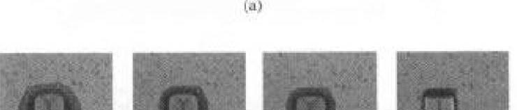
7 Aspect ratio = ratio of the depth to the width of hole / structure
8 MEMS Semiconductors as mechanical materials Bulk micromachining Dry etching Wet etching Surface micromachining MUMPs Polymer MEMS Wafer bonding
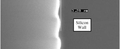
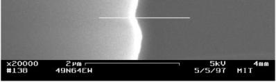
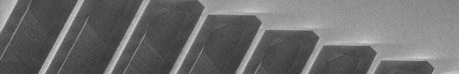
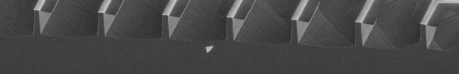
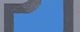
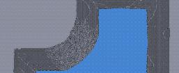
9 Bulk micromachining Dry etching Deep reactive ion etching (DRIE) Inductively coupled plasma (ICP): The Bosch process Wet etching Isotropic (HNA) Anisotropic (KOH, TMAH,...)
10 Reactant DRY Etching - principle Products Mask Bombardment Impulse transfer Physical etching (a) Film/substrate Reactant Products Mask Chemical etching Adsorption Reaction Desorption Reactant Products (b) Mask Adsorption Desorption Ion-enhanced reaction Synergetical (c)


11 Chemical: isotropic etching E.g. XeF 2 or SF 6
12 Physical: tapered etching

13 Physical: tapered etching
14 Synergetical: vertical etching


15 Synergetical: vertical etching

16 Typical etching

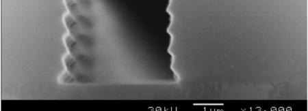


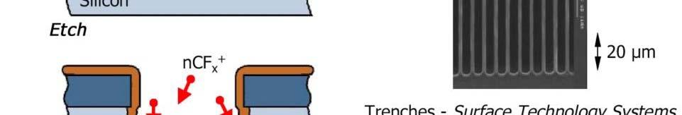

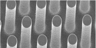
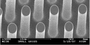
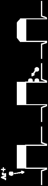
17 The Bosch process
18 Cryogenic DRIE Principle SF 6 /O 2 plasma At cryogenic temperatures (T < -100 C), a passivating SiO x F y layer forms on top of the silicon surface sputtered away from horizontal surfaces by directional ion bombardment. thickness of the passivation layer is mainly determined by the O 2 flow rate (more O 2, more passivation) Superior sidewall quality
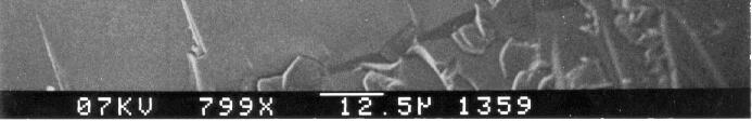
19


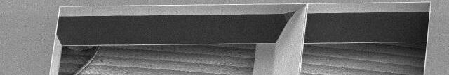
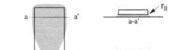
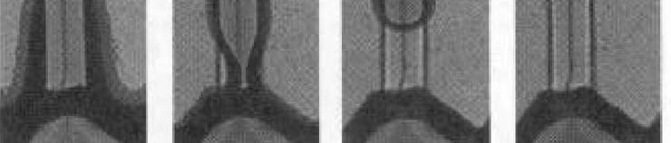
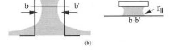
20 Artifacts in dry etching Notching (ion trajectory distortion & chemical etching) RIE lag or ARDE Aspect ratio dependent etching Faceting, Ditching (Trenching) and Redeposition
21 Advanced dry etching (1)
22 Advanced dry etching (2)
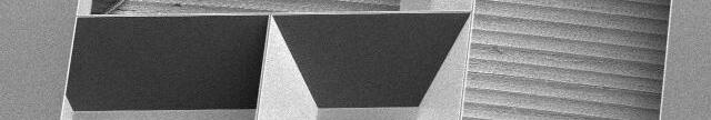
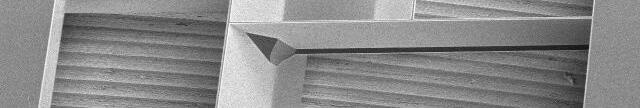
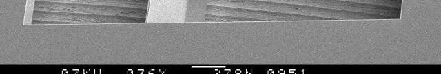
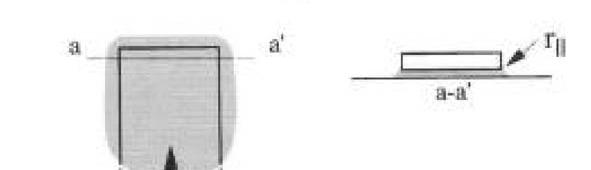
23 Typical RIE Gases Material Typical etchant Typical etch rate (µm/min) Typical mask Si SF 6 BCl 3 + Cl 2 ~ 3-8(DRIE) ~ 0.5 Photo resist, SiO 2, Al SiO 2 CF 4 ~ 0.02 Photo resist, Al 2 4 Si 3 N 4 CHF 3 ~ Photo resist, Al GaAs CCl 2 F 2 + O 2 ~ 0.2 Ni, Al, Cr SiC SF 6 ~ Photo resist, Al Al Cl 2 ~ 0.3 Photo resist Au CCl 2 F 2 ~ 0.05 Photo resist
24 Wet etching Isotropic etching Same etch rate in all directions Lateral etch rate is about the same as vertical etch rate Etch rate does not depend upon the orientation of the mask edge Anisotropic etching Etch rate depends upon orientation to crystalline planes Lateral etch rate can be much larger or smaller than vertical etch rate, depending upon orientation of mask edge to crystalline axes Orientation of mask edge and the details of the mask pattern determine the final etched shape Can be very useful for making complex shapes Can be very surprising if not carefully thought out Only certain standard shapes are routinely used Much cheaper than dry etching techniques Higher safety risk for lab personnel: bases & acids instead of confined plasma
25 Crystal planes in silicon Silicon: Face Centered Cubic (FCC) [100] [111] [010] [001]
26 Anisotropic wet etching - orientation dependent etching Si
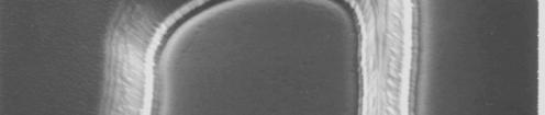
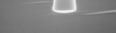
27 <100>

28 Si
29 <011>


30 Anisotropic wet etching: AFM tips resistors Tip connection Cristina 300 μm Rusu
31 KOH Comparatively safe and non-toxic High crystal plane selectivity Limited SiO 2 selectivity Not CMOS compatible: potassium (K) Careful cleaning can allow KOH-etched wafers (Piranha cleaning) in not too picky CMOS facilities
32 Tetra-Methyl Ammonium Hydroxide (TMAH) CMOS compatible Lower crystal plane selectivity: (111):(011):(100) 1:60:20 High selectivity towards SiO 2 Poison, oso,corrosiveos
33 Crystal alignment Identifying the correct crystal alignment Flat alignment: ±1º (standard) Test etch + alignment Alignment forks (Vangbo and Bäcklund): ±0.05º
34 Misalignment in orientation dependent etching <011> Wafer flat <100> <111>
35 Misalignment in orientation dependent etching Wafer flat 5 o
36 Misalignment in orientation dependent etching Wafer flat 45 o

")
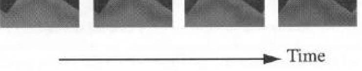
37 Alignment forks (Vangbo & Bäcklund)
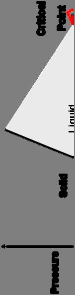
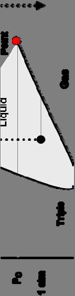
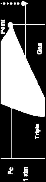
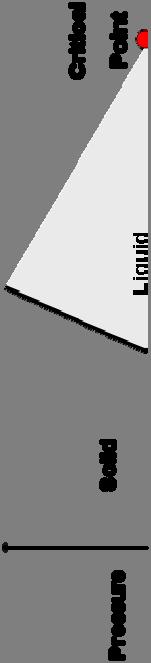
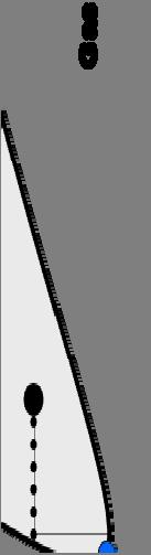
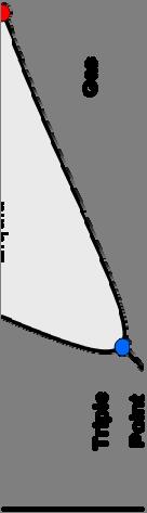
38 Corner compensation structures
39 Solution: corner compensation structures
40 Simulation software Cellular automata-based simulation 3D continuous Intellisuite AnisE Fast Does not simulate surface roughness Monte Carlo CoventorWare: Etch3D Advantage: precise Slow, heavy on resources (memory, cpu)
41 AnisE
42 CoventorWare Etch3d 1406µm 575µm 700µm 575µm 140µm 500µm 575µm 290µm
43 MEMS Semiconductors as mechanical materials Bulk micromachining Dry etching Wet etching Surface micromachining Stiction Lithophraphy MUMPs Polymer MEMS Wafer bonding

44 Evaporation Drying - Stiction

45 Stiction = Big problem in MEMS Capillary force greater than structural stiffness The microstructures may remain stuck to substrate even after dry. Cause: solid bridging, van der Waals force, electrostatic force, hydrogen bonding, etc
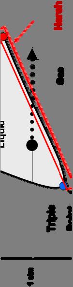


46 Evaporation Drying Supercritical Drying Sublimation Drying Material Tc (ºC) Pc (atm) Pc (psi) Water Methanol CO Vapour phase Etching T-butyl alcohol freezes at 26 ºC P-dichlorobenzene freezes at 56 ºC Anhydrous HF vapour avoiding liquid-gas transition


47 Stiction Reduction Strategies Reduce Adhesion Area dimples surface roughening low surface-energy coatings Integrate supporting microstructures increase tolerance of capillary forces Examples: microtethers microfuses sacrificial i supporting layers (ex. photoresist) t) coat devices with low surface-energy films


48 Lithography issues MEMS: often large height differences Spray coating Proximity exposure Still lower resolution
49 Surface micromachining, e.g. polymumps Cost per submission is $3,200/academic, $4,500/commercial 1cm 2 die area per submission 15 identical dice returned (~$2/mm 2 ) Dicing, bonding, HF release are all available for additional cost Parameterized and static design cells are free online Design services are available for additional cost 2-5 weeks time to evaluate/test chips and revise design for next scheduled run
50 polymumps process flow
51 polymumps process flow
52 polymumps process flow


53 Example IR microspectrometer
54 Different MUMPs processes PolyMUMPs 8 lithography levels, 7 physical layers 3 Poly layers 1 Metal layer SOIMUMPs 10 or 20 µm structure layer Double-sided pattern/etch 2 Metal layers MetalMUMPs 10 lithography layers Thick electroplated Ni (18-22 µm) Source: MEMSCAP
55 MEMS Semiconductors as mechanical materials Bulk micromachining Surface micromachining Polymer MEMS Wafer bonding
56 Polymer MEMS Fabrication methods Polymers Parylene PDMS Paraffin Polyimide, BCB SU-8 PMMA...
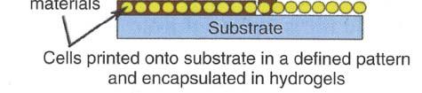
57 Polymer fabrication methods (1) Injection moulding Hot embossing Casting

58 Polymer fabrication methods (2) Stereolithography Ink jet printing
59 Parylene Poly-para-xylylene Vapor-phase deposition Low-temperature t process (<100ºC) Very conformal (~100mbar) Advantages: Low surface roughness Stress free Excellent dielectric breakdown properties <1µm Pinhole free for film thicknesses >0.5µm Low autofluorescence Biocompatible Adhesion: Silanization recommended for Si, Si 3 N 4, SiO 2 and Al surfaces O 2 plasma treatment recommended for polymer surfaces No preparation required for Cr, Au, Ti Microfabrication Etched using O 2 and CF 4 atmosphere


60 PDMS Polydimethylsiloxane Silicone Not allowed at MC2 Biocompatible Can be spun or poured on mold Easily bonded to PDMS, Si, SiO 2 using O 2 plasma activation Low cost
61 Paraffin Properties Low thermal conductivity Low electrical conductivity Low chemical reactivity High thermal expansion during phase change High boiling point Applications Microactuators
62 Polyimide & Benzo cyclobutene (BCB) PI: Kapton Spin-on Patterning Photopatternable (negative) storage temperatures < -25ºC Etchable (O 2 plasma) Advantages Chemical & thermal stability Low water uptake Biocompatibility (PI) Multilayer deposition
63 SU-8 Negative photoresist (UV) High aspect ratios (>18) can be obtained Higher aspect ratios (>60) with synchrotron X-ray Can be used as mold or as structural material
")
64 PMMA Polymethylmethacrylate (Plexiglass) X-ray patternable Aspect ratios: (freestanding-supported) when applied in LIGA µm thick (Also used as e-beam resist, but a slightly lower thicknesses) LIGA
65 Other materials Hydrogels Good for chemical sensing applications Biodegradable materials Polyglycolic acide (PGA), polylactic acid (PLDA),... Fabrication methods: imprinting, hot embossing, stereolithography, laser micromachining
66 MEMS Semiconductors as mechanical materials Bulk micromachining Dry etching Wet etching Surface micromachining MUMPs Polymer MEMS Wafer bonding
MEMS Fabrication. Beyond Integrated Circuits. MEMS Basic Concepts
 MEMS Fabrication Beyond Integrated Circuits MEMS Basic Concepts Uses integrated circuit fabrication techniques to make mechanical as well as electrical components on a single chip. Small size 1µm 1mm Typically
Manufacturing Technologies for MEMS and SMART SENSORS
 4 Manufacturing Technologies for MEMS and SMART SENSORS Dr. H. K. Verma Distinguished Professor (EEE) Sharda University, Greater Noida (Formerly: Deputy Director and Professor of Instrumentation Indian
Solid State Sensors. Microfabrication 8/22/08 and 8/25/08
 Solid State Sensors Microfabrication 8/22/08 and 8/25/08 Purpose of This Material To introduce the student to microfabrication techniques as used to fabricate MEMS Sensors Understand concepts not specifics
Surface Micromachining
 Surface Micromachining Outline Introduction Material often used in surface micromachining Material selection criteria in surface micromachining Case study: Fabrication of electrostatic motor Major issues
Today s Class. Materials for MEMS
 Lecture 2: VLSI-based Fabrication for MEMS: Fundamentals Prasanna S. Gandhi Assistant Professor, Department of Mechanical Engineering, Indian Institute of Technology, Bombay, Recap: Last Class What is
ME 189 Microsystems Design and Manufacture. Chapter 9. Micromanufacturing
 ME 189 Microsystems Design and Manufacture Chapter 9 Micromanufacturing This chapter will offer an overview of the application of the various fabrication techniques described in Chapter 8 in the manufacturing
There are basically two approaches for bulk micromachining of. silicon, wet and dry. Wet bulk micromachining is usually carried out
 57 Chapter 3 Fabrication of Accelerometer 3.1 Introduction There are basically two approaches for bulk micromachining of silicon, wet and dry. Wet bulk micromachining is usually carried out using anisotropic
Surface Micromachining
 Surface Micromachining Micro Actuators, Sensors, Systems Group University of Illinois at Urbana-Champaign Outline Definition of surface micromachining Most common surface micromachining materials - polysilicon
L5: Micromachining processes 1/7 01/22/02
 97.577 L5: Micromachining processes 1/7 01/22/02 5: Micromachining technology Top-down approaches to building large (relative to an atom or even a transistor) structures. 5.1 Bulk Micromachining A bulk
EE C245 ME C218 Introduction to MEMS Design Fall 2011
 Lecture Outline EE C245 ME C218 Introduction to MEMS Design Fall 2011 Prof. Clark T.-C. Nguyen Dept. of Electrical Engineering & Computer Sciences University of California at Berkeley Berkeley, CA 94720
Mikrosensorer. Microfabrication 1
 Mikrosensorer Microfabrication 1 Literature Introductory MEMS Fabrication and Applications Thomas M. Adams and Richard A. Layton Available as ebook on http://www.lub.lu.se/en/search/lubsearch.html This
General Introduction to Microstructure Technology p. 1 What is Microstructure Technology? p. 1 From Microstructure Technology to Microsystems
 General Introduction to Microstructure Technology p. 1 What is Microstructure Technology? p. 1 From Microstructure Technology to Microsystems Technology p. 9 The Parallels to Microelectronics p. 15 The
Surface micromachining and Process flow part 1
 Surface micromachining and Process flow part 1 Identify the basic steps of a generic surface micromachining process Identify the critical requirements needed to create a MEMS using surface micromachining
Lecture 5. SOI Micromachining. SOI MUMPs. SOI Micromachining. Silicon-on-Insulator Microstructures. Agenda:
 EEL6935 Advanced MEMS (Spring 2005) Instructor: Dr. Huikai Xie SOI Micromachining Agenda: SOI Micromachining SOI MUMPs Multi-level structures Lecture 5 Silicon-on-Insulator Microstructures Single-crystal
Chapter 4 Fabrication Process of Silicon Carrier and. Gold-Gold Thermocompression Bonding
 Chapter 4 Fabrication Process of Silicon Carrier and Gold-Gold Thermocompression Bonding 4.1 Introduction As mentioned in chapter 2, the MEMs carrier is designed to integrate the micro-machined inductor
Micro-Electro-Mechanical Systems (MEMS) Fabrication. Special Process Modules for MEMS. Principle of Sensing and Actuation
 Fabrication. Special Process Modules for MEMS. Principle of Sensing and Actuation") Micro-Electro-Mechanical Systems (MEMS) Fabrication Fabrication Considerations Stress-Strain, Thin-film Stress, Stiction Special Process Modules for MEMS Bonding, Cavity Sealing, Deep RIE, Spatial forming
Micro-Electro-Mechanical Systems (MEMS) Fabrication Fabrication Considerations Stress-Strain, Thin-film Stress, Stiction Special Process Modules for MEMS Bonding, Cavity Sealing, Deep RIE, Spatial forming
IC/MEMS Fabrication - Outline. Fabrication
 IC/MEMS Fabrication - Outline Fabrication overview Materials Wafer fabrication The Cycle: Deposition Lithography Etching Fabrication IC Fabrication Deposition Spin Casting PVD physical vapor deposition
Outline. Introduction to the LIGA Microfabrication Process. What is LIGA? The LIGA Process. Dr. Bruce K. Gale Fundamentals of Microfabrication
 Outline Introduction to the LIGA Microfabrication Process Dr. Bruce K. Gale Fundamentals of Microfabrication What is LIGA? The LIGA Process Lithography Techniques Electroforming Mold Fabrication Analyzing
Regents of the University of California
 Surface-Micromachining Process Flow Photoresist Sacrificial Oxide Structural Polysilcon Deposit sacrificial PSG: Target = 2 m 1 hr. 40 min. LPCVD @450 o C Densify the PSG Anneal @950 o C for 30 min. Lithography
Lecture 10: MultiUser MEMS Process (MUMPS)
") MEMS: Fabrication Lecture 10: MultiUser MEMS Process (MUMPS) Prasanna S. Gandhi Assistant Professor, Department of Mechanical Engineering, Indian Institute of Technology, Bombay, 1 Recap Various VLSI based
MEMS: Fabrication Lecture 10: MultiUser MEMS Process (MUMPS) Prasanna S. Gandhi Assistant Professor, Department of Mechanical Engineering, Indian Institute of Technology, Bombay, 1 Recap Various VLSI based
Chemical Vapor Deposition
 Chemical Vapor Deposition ESS4810 Lecture Fall 2010 Introduction Chemical vapor deposition (CVD) forms thin films on the surface of a substrate by thermal decomposition and/or reaction of gas compounds
INF5490 RF MEMS. LN02: MEMS Fabrication. Spring 2012, Oddvar Søråsen Department of Informatics, UoO
 INF5490 RF MEMS LN02: MEMS Fabrication Spring 2012, Oddvar Søråsen Department of Informatics, UoO 1 Micromachining Today s lecture Important process steps General Summary: MEMS-specific steps Examples
Semiconductor Manufacturing Process 10/11/2005
 Semiconductor Manufacturing Process 10/11/2005 Photolithography Oxidation CVD PVD Photolithography The purpose of photolithography is to imprint the desired pattern of a micro component on a substrate,
Micro-Electro-Mechanical Systems (MEMS) Fabrication. Special Process Modules for MEMS. Principle of Sensing and Actuation
 Fabrication. Special Process Modules for MEMS. Principle of Sensing and Actuation") Micro-Electro-Mechanical Systems (MEMS) Fabrication Fabrication Considerations Stress-Strain, Thin-film Stress, Stiction Special Process Modules for MEMS Bonding, Cavity Sealing, Deep RIE, Spatial forming
Micro-Electro-Mechanical Systems (MEMS) Fabrication Fabrication Considerations Stress-Strain, Thin-film Stress, Stiction Special Process Modules for MEMS Bonding, Cavity Sealing, Deep RIE, Spatial forming
Ultrasonic Micromachining in the fabrication of MEMS Micro-sensors
 Ultrasonic Micromachining in the fabrication of MEMS Micro-sensors Jamil Akhtar Professor AcSIR New Delhi Chief Scientist & Head, CSIR-CEERI, Pilani, INDIA CEERI, Pilani A constituent laboratory of CSIR,
Chapter 2 OVERVIEW OF MEMS
 6 Chapter 2 OVERVIEW OF MEMS 2.1 MEMS and Microsystems The term MEMS is an abbreviation of microelectromechanical system. MEMS contains components ofsizes in 1 micrometer to 1 millimeter. The core element
Soft Lithography: MIMIC. Micro Contact Printing. Microtransfer Molding. Soft Lithography: Replica Molding. Soft Lithography.
 Can We Measure Everything? Microfabrication Using Polymers Dr. Bruce K. Gale ENGR 494C and 594C Polymers for Microfabrication Examples diverse PDMS PMMA Polyurethane Polyimide Polystyrene Disadvantages
Fabrication Technology, Part I
 EEL5225: Principles of MEMS Transducers (Fall 2003) Fabrication Technology, Part I Agenda: Oxidation, layer deposition (last lecture) Lithography Pattern Transfer (etching) Impurity Doping Reading: Senturia,
Micro-Electro-Mechanical Systems (MEMS) Fabrication. Special Process Modules for MEMS. Principle of Sensing and Actuation
 Fabrication. Special Process Modules for MEMS. Principle of Sensing and Actuation") Micro-Electro-Mechanical Systems (MEMS) Fabrication Fabrication Considerations Stress-Strain, Thin-film Stress, Stiction Special Process Modules for MEMS Bonding, Cavity Sealing, Deep RIE, Spatial forming
Micro-Electro-Mechanical Systems (MEMS) Fabrication Fabrication Considerations Stress-Strain, Thin-film Stress, Stiction Special Process Modules for MEMS Bonding, Cavity Sealing, Deep RIE, Spatial forming
Fabrication Technology, Part II
 EEL5225: Principles of MEMS Transducers (Fall 2003) Fabrication Technology, Part II Agenda: Process Examples TI Micromirror fabrication process SCREAM CMOS-MEMS processes Wafer Bonding LIGA Reading: Senturia,
PHYS 534 (Fall 2008) Process Integration OUTLINE. Examples of PROCESS FLOW SEQUENCES. >Surface-Micromachined Beam
 Process Integration OUTLINE. Examples of PROCESS FLOW SEQUENCES. >Surface-Micromachined Beam") PHYS 534 (Fall 2008) Process Integration Srikar Vengallatore, McGill University 1 OUTLINE Examples of PROCESS FLOW SEQUENCES >Semiconductor diode >Surface-Micromachined Beam Critical Issues in Process
PHYS 534 (Fall 2008) Process Integration Srikar Vengallatore, McGill University 1 OUTLINE Examples of PROCESS FLOW SEQUENCES >Semiconductor diode >Surface-Micromachined Beam Critical Issues in Process
Lecture 5: Micromachining
 MEMS: Fabrication Lecture 5: Micromachining Prasanna S. Gandhi Assistant Professor, Department of Mechanical Engineering, Indian Institute of Technology, Bombay, Recap: Last Class E-beam lithography X-ray
6.777J/2.732J Design and Fabrication of Microelectromechanical Devices Spring Term Solution to Problem Set 2 (16 pts)
") 6.777J/2.732J Design and Fabrication of Microelectromechanical Devices Spring Term 2007 By Brian Taff (Adapted from work by Feras Eid) Solution to Problem Set 2 (16 pts) Issued: Lecture 4 Due: Lecture
6.777J/2.732J Design and Fabrication of Microelectromechanical Devices Spring Term 2007 By Brian Taff (Adapted from work by Feras Eid) Solution to Problem Set 2 (16 pts) Issued: Lecture 4 Due: Lecture
Micromachining AMT 2505
 Micromachining AMT 2505 Shanmuga Raja.B (BVB0912004) Module leader : Mr. Raja Hussain Introduction Micromachining are inherently connected to the evolution of Micro Electro Mechanical Systems (MEMS). Decades
Lecture 22: Integrated circuit fabrication
 Lecture 22: Integrated circuit fabrication Contents 1 Introduction 1 2 Layering 4 3 Patterning 7 4 Doping 8 4.1 Thermal diffusion......................... 10 4.2 Ion implantation.........................
Lect. 2: Basics of Si Technology
 Unit processes Thin Film Deposition Etching Ion Implantation Photolithography Chemical Mechanical Polishing 1. Thin Film Deposition Layer of materials ranging from fractions of nanometer to several micro-meters
Regents of the University of California 1
 Electroplating: Metal MEMS Nickel Surface-Micromachining Process Flow Photoresist Wafer Release Etchant Use electroplating to obtain metal μstructures When thick: call it LIGA Pros: fast low temp deposition,
Review of CMOS Processing Technology
 - Scaling and Integration Moore s Law Unit processes Thin Film Deposition Etching Ion Implantation Photolithography Chemical Mechanical Polishing 1. Thin Film Deposition Layer of materials ranging from
EE C245 ME C218 Introduction to MEMS Design Fall 2007
 EE C245 ME C218 Introduction to MEMS Design Fall 2007 Prof. Clark T.-C. Nguyen Dept. of Electrical Engineering & Computer Sciences University of California at Berkeley Berkeley, CA 94720 Lecture 10: Bulk
Journal of Advanced Mechanical Design, Systems, and Manufacturing
 Fabrication of the X-Ray Mask using the Silicon Dry Etching * Hiroshi TSUJII**, Kazuma SHIMADA**, Makoto TANAKA**, Wataru YASHIRO***, Daiji NODA** and Tadashi HATTORI** **Laboratory of Advanced Science
Polymer Microfabrication (Part II) Prof. Tianhong Cui, Mechanical Engineering ME 8254
 Prof. Tianhong Cui, Mechanical Engineering ME 8254") Polymer Microfabrication (Part II) Prof. Tianhong Cui, Mechanical Engineering ME 8254 Other Polymer Techniques Embossing Low cost High throughput Structures as small as 25 nm Injection molding Features
Polymer Microfabrication (Part II) Prof. Tianhong Cui, Mechanical Engineering ME 8254 Other Polymer Techniques Embossing Low cost High throughput Structures as small as 25 nm Injection molding Features
Multiple-height Microstructures Fabricated by ICP-RIE and Embedded Masking Layers
 Paper Multiple-height Microstructures Fabricated by ICP-RIE and Embedded Masking Layers Student Member Makoto Mita (IIS., Univ. of Tokyo & CREST/JST ) Student Member Yoshio Mita (IIS., Univ. of Tokyo)
Regents of the University of California
 Topography Issues Degradation of lithographic resolution PR step coverage, streaking Thickness differences pose problems for reduction steppers Direction of Spin PR PR PR Stringers Problematic when using
EECS130 Integrated Circuit Devices
 EECS130 Integrated Circuit Devices Professor Ali Javey 9/13/2007 Fabrication Technology Lecture 1 Silicon Device Fabrication Technology Over 10 15 transistors (or 100,000 for every person in the world)
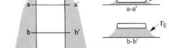
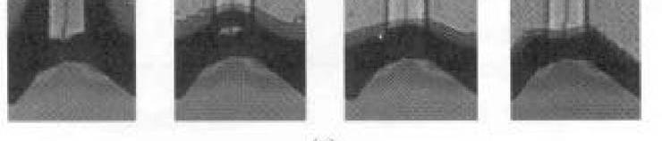
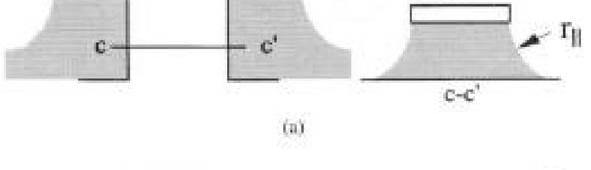
Tapered Walls Via Holes Manufactured Using DRIE Variable Isotropy Process
 Tapered Walls Via Holes Manufactured Using DRIE Variable Isotropy Process D. VASILACHE, S. RONCHIN, S. COLPO, B. MARGESIN, F. GIACOMOZZI, S. GENNARO FBK-irst, via Sommarive 18-38123 Trento, Italy; Tel.:
Supporting Information: Model Based Design of a Microfluidic. Mixer Driven by Induced Charge Electroosmosis
 Supporting Information: Model Based Design of a Microfluidic Mixer Driven by Induced Charge Electroosmosis Cindy K. Harnett, Yehya M. Senousy, Katherine A. Dunphy-Guzman #, Jeremy Templeton * and Michael
Introduction to Micro/Nano Fabrication Techniques. Date: 2015/05/22 Dr. Yi-Chung Tung. Fabrication of Nanomaterials
 Introduction to Micro/Nano Fabrication Techniques Date: 2015/05/22 Dr. Yi-Chung Tung Fabrication of Nanomaterials Top-Down Approach Begin with bulk materials that are reduced into nanoscale materials Ex:
Atomic Layer Deposition(ALD)
") Atomic Layer Deposition(ALD) AlO x for diffusion barriers OLED displays http://en.wikipedia.org/wiki/atomic_layer_deposition#/media/file:ald_schematics.jpg Lam s market-leading ALTUS systems combine CVD
Atomic Layer Deposition(ALD) AlO x for diffusion barriers OLED displays http://en.wikipedia.org/wiki/atomic_layer_deposition#/media/file:ald_schematics.jpg Lam s market-leading ALTUS systems combine CVD
Preface Preface to First Edition
 Contents Foreword Preface Preface to First Edition xiii xv xix CHAPTER 1 MEMS: A Technology from Lilliput 1 The Promise of Technology 1 What Are MEMS or MST? 2 What Is Micromachining? 3 Applications and
A discussion of crystal growth, lithography, etching, doping, and device structures is presented in
 Chapter 5 PROCESSING OF DEVICES A discussion of crystal growth, lithography, etching, doping, and device structures is presented in the following overview gures. SEMICONDUCTOR DEVICE PROCESSING: AN OVERVIEW
SURFACE MICROMACHINING
 SURFACE MICROMACHINING Features are built up, layer by layer on the surface of a substrate. Surface micromachined devices are much smaller than bulk micromachined components. Nature of deposition process
Procese de depunere in sistemul Plasma Enhanced Chemical Vapor Deposition (PECVD)
") Procese de depunere in sistemul Plasma Enhanced Chemical Vapor Deposition (PECVD) Ciprian Iliescu Conţinutul acestui material nu reprezintă in mod obligatoriu poziţia oficială a Uniunii Europene sau a
Procese de depunere in sistemul Plasma Enhanced Chemical Vapor Deposition (PECVD) Ciprian Iliescu Conţinutul acestui material nu reprezintă in mod obligatoriu poziţia oficială a Uniunii Europene sau a
Chapter 3 Silicon Device Fabrication Technology
 Chapter 3 Silicon Device Fabrication Technology Over 10 15 transistors (or 100,000 for every person in the world) are manufactured every year. VLSI (Very Large Scale Integration) ULSI (Ultra Large Scale
Plasma Etching Rates & Gases Gas ratios affects etch rate & etch ratios to resist/substrate
 Plasma Etching Rates & Gases Gas ratios affects etch rate & etch ratios to resist/substrate Development of Sidewalls Passivating Films Sidewalls get inert species deposited on them with plasma etch Creates
Czochralski Crystal Growth
 Czochralski Crystal Growth Crystal Pulling Crystal Ingots Shaping and Polishing 300 mm wafer 1 2 Advantage of larger diameter wafers Wafer area larger Chip area larger 3 4 Large-Diameter Wafer Handling
Micromachining vs. Soft Fabrication
 Introduction to BioMEMS & Medical Microdevices Silicon Microfabrication Part 1 Companion lecture to the textbook: Fundamentals of BioMEMS and Medical Microdevices, by Prof., http://saliterman.umn.edu/
Thin. Smooth. Diamond.
 UNCD Wafers Thin. Smooth. Diamond. UNCD Wafers - A Family of Diamond Material UNCD is Advanced Diamond Technologies (ADT) brand name for a family of thin fi lm diamond products. UNCD Aqua The Aqua series
Thin. Smooth. Diamond.
 UNCD Wafers Thin. Smooth. Diamond. UNCD Wafers - A Family of Diamond Material UNCD is Advanced Diamond Technologies (ADT) brand name for a family of thin fi lm diamond products. UNCD Aqua The Aqua series
MEMS Fabrication I : Process Flows and Bulk Micromachining
 MEMS Fabrication I : Process Flows and Bulk Micromachining Dr. Thara Srinivasan Lecture 2 Picture credit: Alien Technology Lecture Outline Reading Reader is in! (at South side Copy Central) Kovacs, Bulk
applied to Biomedical Instrumentation Microfabrication and Nanofabrication Microtechnology Nanotechnology Biomedical Lecture 9 and
 Lecture 9 Biomedical Microtechnology and Nanotechnology Microfabrication and Nanofabrication applied to Biomedical Instrumentation Why Micro/Nano? SCALING OF PARAMETERS The values of various parameters
EE C245 ME C218 Introduction to MEMS Design
 EE C245 ME C218 Introduction to MEMS Design Fall 2007 Prof. Clark T.-C. Nguyen Dept. of Electrical Engineering & Computer Sciences University of California at Berkeley Berkeley, CA 94720 Lecture 10: Surface
Plasma Etching Rates & Gases Gas ratios affects etch rate & etch ratios to resist/substrate
 Plasma Etching Rates & Gases Gas ratios affects etch rate & etch ratios to resist/substrate Development of Sidewalls Passivating Films Sidewalls get inert species deposited on them with plasma etch Creates
Polymer-based Microfabrication
 Polymer-based Microfabrication PDMS SU-8 PMMA Hydrogel 1 Soft Lithography Developed by Whitesides, et. al A set of techniques for microfabrication based on the use of lithography, soft substrate materials
SOIMUMPs Design Handbook
 SOIMUMPs Design Handbook a MUMPs process C. J. Han, Allen Cowen, Greg Hames and Busbee Hardy MEMScAP Revision 3.0 Copyright 2002 by MEMScAP. All rights reserved. Permission to use and copy for internal,
ENG/PHYS3320 Microsystems Technology Chapter 2 Fabrication of Microsystems
 ENG/PHYS3320 Microsystems Technology Chapter 2 Fabrication of Microsystems ENG/PHYS3320: R.I. Hornsey Fab: 1 Fabrication Many of the new transducers are based on a technology known as micromachining a
A Quick Overview of Micromachining for MEMS Designers
 A Quick Overview of Micromachining for MEMS Designers A designer has control over two sets of variables: materials and the shapes of parts. M. F. Ashby Manufacturing determines which materials can be processed
Cost Effective 3D Glass Microfabrication for Advanced Packaging Applications
 Cost Effective 3D Glass Microfabrication for Advanced Packaging Applications Authors: Jeb. H Flemming, Kevin Dunn, James Gouker, Carrie Schmidt, Roger Cook ABSTRACT Historically, while glasses have many
Fabrication and Layout
 ECEN454 Digital Integrated Circuit Design Fabrication and Layout ECEN 454 3.1 A Glimpse at MOS Device Polysilicon Aluminum ECEN 475 4.2 1 Material Classification Insulators Glass, diamond, silicon oxide
4/10/2012. Introduction to Microfabrication. Fabrication
 Introduction to Microfabrication Fabrication 1 MEMS Fabrication Flow Basic Process Flow in Micromachining Nadim Maluf, An introduction to Microelectromechanical Systems Engineering 2 Thin Film Deposition
Mostafa Soliman, Ph.D. May 5 th 2014
 Mostafa Soliman, Ph.D. May 5 th 2014 Mostafa Soliman, Ph.D. 1 Basic MEMS Processes Front-End Processes Back-End Processes 2 Mostafa Soliman, Ph.D. Wafers Deposition Lithography Etch Chips 1- Si Substrate
3. Overview of Microfabrication Techniques
 3. Overview of Microfabrication Techniques The Si revolution First Transistor Bell Labs (1947) Si integrated circuits Texas Instruments (~1960) Modern ICs More? Check out: http://www.pbs.org/transistor/background1/events/miraclemo.html
Dr. Lynn Fuller Webpage:
 ROCHESTER INSTITUTE OF TECHNOLOGY MICROELECTRONIC ENGINEERING Microelectromechanical Systems (MEMs) Process Integration Dr. Lynn Fuller Webpage: http://people.rit.edu/lffeee 82 Lomb Memorial Drive Rochester,
EE C245 ME C218 Introduction to MEMS Design Fall 2011
 Lecture Outline EE C245 ME C218 Introduction to MEMS Design Fall 2011 Prof. Clark T.-C. Nguyen Dept. of Electrical Engineering & Computer Sciences University of California at Berkeley Berkeley, CA 94720
Wireless implantable chip with integrated Nitinol-based pump for radio-controlled local drug delivery
 Electronic Supplementary Material (ESI) for Lab on a Chip. This journal is The Royal Society of Chemistry 2014 Electronic Supplementary Information Wireless implantable chip with integrated Nitinol-based
EE 5344 Introduction to MEMS. CHAPTER 3 Conventional Si Processing
 3. Conventional licon Processing Micromachining, Microfabrication. EE 5344 Introduction to MEMS CHAPTER 3 Conventional Processing Why silicon? Abundant, cheap, easy to process. licon planar Integrated
Chapter 2 Manufacturing Process
 Digital Integrated Circuits A Design Perspective Chapter 2 Manufacturing Process 1 CMOS Process 2 CMOS Process (n-well) Both NMOS and PMOS must be built in the same silicon material. PMOS in n-well NMOS
Physical Vapor Deposition (PVD) Zheng Yang
 Zheng Yang") Physical Vapor Deposition (PVD) Zheng Yang ERF 3017, email: yangzhen@uic.edu Page 1 Major Fabrication Steps in MOS Process Flow UV light Mask oxygen Silicon dioxide photoresist exposed photoresist oxide
Physical Vapor Deposition (PVD) Zheng Yang ERF 3017, email: yangzhen@uic.edu Page 1 Major Fabrication Steps in MOS Process Flow UV light Mask oxygen Silicon dioxide photoresist exposed photoresist oxide
Applications of High-Performance MEMS Pressure Sensors Based on Dissolved Wafer Process
 Applications of High-Performance MEMS Pressure Sensors Based on Dissolved Wafer Process Srinivas Tadigadapa and Sonbol Massoud-Ansari Integrated Sensing Systems (ISSYS) Inc., 387 Airport Industrial Drive,
Plasma Etching Rates & Gases Gas ratios affects etch rate & etch ratios to resist/substrate
 Plasma Etching Rates & Gases Gas ratios affects etch rate & etch ratios to resist/substrate Development of Sidewalls Passivating Films Sidewalls get inert species deposited on them with plasma etch Creates
Gaetano L Episcopo. Introduction to MEMS
 Gaetano L Episcopo Introduction to MEMS What are MEMS? Micro Electro Mechanichal Systems MEMS are integrated devices, or systems of devices, with microscopic parts, such as: Mechanical Parts Electrical
EE C245 ME C218 Introduction to MEMS Design Fall 2007
 EE C245 ME C218 Introduction to MEMS Design Fall 2007 Prof. Clark T.-C. Nguyen Dept. of Electrical Engineering & Computer Sciences University of California at Berkeley Berkeley, CA 94720 Lecture 9: Surface
A High Speed Surface Illuminated Si Photodiode. Using Microstructured Holes for Absorption. Enhancements at nm wavelength
 A High Speed Surface Illuminated Si Photodiode Using Microstructured Holes for Absorption Enhancements at 900 1000 nm wavelength Supporting Information Yang Gao, Hilal Cansizoglu, Soroush Ghandiparsi,
Compact hybrid plasmonic-si waveguide structures utilizing Albanova E-beam lithography system
 Compact hybrid plasmonic-si waveguide structures utilizing Albanova E-beam lithography system Introduction Xu Sun Laboratory of Photonics and Microwave Engineering, Royal Institute of Technology (KTH),
The Berkeley Marvell NanoLab
 The History The Berkeley Marvell NanoLab The Culture The Present The BNLA The Capabilities The End MEMS Industry Group M2M 20May2014 Bill Flounders, Ph.D. NanoLabExecutive Director The History The Berkeley
Advanced Polymers And Resists For Nanoimprint Lithography
 Q U A L I T Y A S S U R A N C E MICROSYSTEMS & NANOSYSTEMS SPECIAL REPORT Advanced Polymers And Resists For Nanoimprint Lithography Numerous polymer systems specifically designed for nanoimprint lithography
5.8 Diaphragm Uniaxial Optical Accelerometer
 5.8 Diaphragm Uniaxial Optical Accelerometer Optical accelerometers are based on the BESOI (Bond and Etch back Silicon On Insulator) wafers, supplied by Shin-Etsu with (100) orientation, 4 diameter and
Thomas M. Adams Richard A. Layton. Introductory MEMS. Fabrication and Applications. Springer
 Thomas M. Adams Richard A. Layton Introductory MEMS Fabrication and Applications Springer Contents Preface xiü Part I Fabrication Chapter 1: Introduction 3 1.1 What are MEMS? 3 1.2 Why MEMS? 4 1.2.1. Low
Lecture 6. Through-Wafer Interconnect. Agenda: Through-wafer Interconnect Polymer MEMS. Through-Wafer Interconnect -1. Through-Wafer Interconnect -2
 Agenda: EEL6935 Advanced MEMS (Spring 2005) Instructor: Dr. Huikai Xie Lecture 6 Through-wafer Interconnect EEL6935 Advanced MEMS 2005 H. Xie 1/21/2005 1 Motivations: Wafer-level packaging CMOS 3D Integration
Plasma Etching Rates & Gases Gas ratios affects etch rate & etch ratios to resist/substrate
 Plasma Etching Rates & Gases Gas ratios affects etch rate & etch ratios to resist/substrate Development of Sidewalls Passivating Films Sidewalls get inert species deposited on them Creates passivating
Lecture 3: Integrated Processes
 Lecture 3: Integrated Processes Single-Crystal Silicon Process Integration Polysilicon Micromachining Process Integrated CMOS Micromachining Process ENE 5400, Spring 2004 1 Single Crystal Silicon ENE 5400,
Chapter 3 CMOS processing technology
 Chapter 3 CMOS processing technology (How to make a CMOS?) Si + impurity acceptors(p-type) donors (n-type) p-type + n-type => pn junction (I-V) 3.1.1 (Wafer) Wafer = A disk of silicon (0.25 mm - 1 mm thick),
Microfabrication Using Silicon Mold Inserts and Hot Embossing
 Microfabrication Using Silicon Mold Inserts and Hot Embossing Liwei Lid), Chun-Jung Chiu'), Walter Bache?) and Mathias Heckele2) ')Institute of Applied Mechanics, National Taiwan University, Taipei, 106,
Microfabrication of Heterogeneous, Optimized Compliant Mechanisms SUNFEST 2001 Luo Chen Advisor: Professor G.K. Ananthasuresh
 Microfabrication of Heterogeneous, Optimized Compliant Mechanisms SUNFEST 2001 Luo Chen Advisor: Professor G.K. Ananthasuresh Fig. 1. Single-material Heatuator with selective doping on one arm (G.K. Ananthasuresh)
Welcome MNT Conference 1 Albuquerque, NM - May 2010
 Welcome MNT Conference 1 Albuquerque, NM - May 2010 Introduction to Design Outline What is MEMs Design General Considerations Application Packaging Process Flow What s available Sandia SUMMiT Overview
Final Project Report. Date Jan. 30 th, To: Kenji Homma, Adaptive Technologies, Blackburgh, Virginia.
 Final Project Report Date Jan. 30 th, 2008 To: Kenji Homma, Adaptive Technologies, Blackburgh, Virginia. By: Zhengchun Peng, Ph.D. candidate Peter Hesketh, Professor School of Mechanical Engineering, Georgia
Cambridge University Press A Guide to Hands-on MEMS Design and Prototyping Joel A. Kubby Excerpt More information.
 1 Introduction 1.1 Overview of MEMS fabrication Microelectromechanical systems (MEMS) fabrication developed out of the thin-film processes first used for semiconductor fabrication. To understand the unique
We are IntechOpen, the world s leading publisher of Open Access books Built by scientists, for scientists. International authors and editors
 We are IntechOpen, the world s leading publisher of Open Access books Built by scientists, for scientists 3,900 116,000 120M Open access books available International authors and editors Downloads Our
MEMS II: January 23. Lab 1: Pop-up mirror - PolyMUMPS - Thermal actuators - Mirror CoventorWare
 MEMS II: January 23 Lab 1: Pop-up mirror - PolyMUMPS - Thermal actuators - Mirror CoventorWare Microelectromechanical Systems (MEMS) Multi-User MEMS Processes (MUMPS) Example Design Anchor hole 2.0 0.5
Thermal Nanoimprinting Basics
 Thermal Nanoimprinting Basics Nanoimprinting is a way to replicate nanoscale features on one surface into another, like stamping copies are made by traditional fabrication techniques (optical/ebeam lith)
4. Process Integration: Case Studies
 Case Study #2: FCantilevered Microgripper Surface Machined MEMS Case Study #2: FCantilevered Microgripper Sandia Lucent Sandia Integrated Accelerometers Optomechanical Systems Integrated Sensors 1 Bulk