Plasma Innovations. Plasma Innovations. PLASMACOAT 3D is the revolutionary dry metallization process for the next generation of polymer electronic
|
|
|
- Francine Sherman
- 6 years ago
- Views:
Transcription


1 Plasma Innovations Plasma Innovations PLASMACOAT 3D is the revolutionary dry metallization process for the next generation of polymer electronic 1

2 The Company Plasma Innovations (PI) and its mother company Inocon Technology are market leaders in manufacturing production equipment for automotive and household appliances based on atmospheric plasma systems. PI is very well positioned in the LED market segment especially concerning the 2-shot molding of heat conductive polymers and the plating-free 3D thick-film plasma metallization. PI is attaining a leading position as technology provider, strategic development partner and supplier of advanced manufacturing equipment for new 3D LED module concepts. 2


3 The Company Regensburg Germany Inocon Group 100 People Family owned Locations: Attnang-Puchheim, Austria Regensburg, German Attnang-Puchheim Austria 3
4 PLASMACOAT 3D PI manufactures and develops Turnkey Solutions for Semiconductor 3D MID LED Antenna 4


5 Plasma Basics What is Plasma? Plasma technology is based on a simple physical principle. Matter changes its state when energy is supplied to it: solids becomes liquid, and liquids becomes gaseous. If even more energy is supplied to a gas, it is ionized and goes into the energy-rich plasma state, the fourth state of matter. 5
6 Plasma Systems PI s µ-plasma PTR Technology MCP Technology Compact metallic layers High conductive layers High deposition efficiency For all thermal sensitive substrates Layer thickness < 50µm Surface Actiation & Cleaning 6

7 Plasma Systems PTR Technology MCP Technology More than 20 years experience in plasma technology! References Audi AG; Daimler AG, Faurecia Exhaust Systems, Fiat,Ford Motor Company, GKN Driveline; General Motors, Porsche, PSA Group, Miele, Siemens 7


8 Substrate Preparation - Surface Cleaning & Activation Surface Preparation of polymer substrates plays a key role for successful metallization! Amorphous glas coating on polymer (10nm) µ-plasma: Reliable ultrafine cleaning with simultaneous high uniform surface coating Complete elimination of solvents containing VOC PlasmaCoat Glas: Surface Coating with silicate layer by atmospheric plasma in nanometer size not coated coated 8
9 Plasma Innovations PLASMACOAT 3D is the revolutionary dry metallization process for the next generation of polymer electronic 9

10 PLASMACOAT 3D The Partners 10
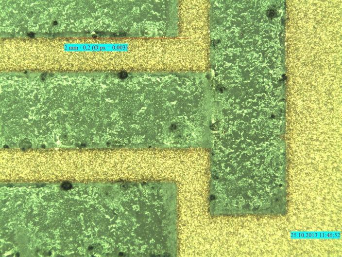
11 Application Sample PLP Process (Paint Laser Plasma) Polymer Metal Powder 11

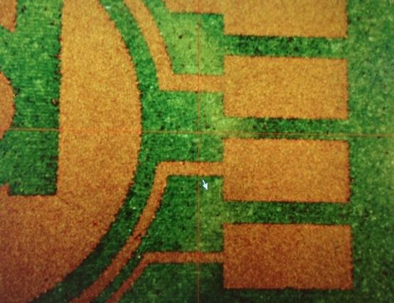
12 Application Sample LED Demonstrator Plasma Innovations 100µm line 12


13 1. Step 2Shot Injection Molding 2-shot material (electrical insulation) 1-shot material (high thermal conductivity) 13

14 2. Step Painting with NON-Stick Lacquer Plasma Innovations Painting Process Non-Stick Lacquer 14

15 NON-STICK Lacquer Masking 3D Laser Structuring - Resolution <50µm - High speed laser structuring - Full 3D solution - Laser direct structuring - Laser structuring of masking lacquers 2D Screen Printing - Resolution <150µm - For flat substrates, films, Roll to Roll 15

16 3. Step Laser Structuring 3D Laser Structuring of Non-Stick Lacquer 16

17 4. Step PLASMACOAT Metallisation Copper PLASMACOAT 3D Metallization Prozess (self structuring) 17


18 4. Step PLASMACOAT Metallisation 2D/3D Plasma Metallization - Layer Thickness 5-500µm - Metalls, Polymers, Ceramic - High Speed Coating - Self Adjusting Structuring Process in Combination with NON-STICK Process 18
")
19 5. Step Pick & Place Assembling of LEDs Plasma Innovations LEDs Pick & Place (Soldering/Bonding) 19
20 PLASMACOAT 3D Polymer Metal Powder 20


21 Thank you very much! See you at Plasma Innovations! 21
NASF SURFACE TECHNOLOGY WHITE PAPERS 83 (1), 7-12 (October 2018) Advances in Decorative PVD Chromium Coatings for Polymer Substrates
, 7-12 (October 2018) Advances in Decorative PVD Chromium Coatings for Polymer Substrates") Advances in Decorative PVD Chromium Coatings for Polymer Substrates A Synopsis * of a Presentation given at SUR/FIN 2018 (Cleveland, Ohio) by Gary Vergason ** Vergason Technology, Inc. Van Etten, New York,
Advances in Decorative PVD Chromium Coatings for Polymer Substrates A Synopsis * of a Presentation given at SUR/FIN 2018 (Cleveland, Ohio) by Gary Vergason ** Vergason Technology, Inc. Van Etten, New York,
Manipulation and control of spatial ALD layers for flexible devices. Aimcal Memphis 2016; Edward Clerkx
 Manipulation and control of spatial ALD layers for flexible devices Meyer Burger Netherlands Equipment manufacturer Functional inkjet printing Based in Eindhoven, the Netherlands Part of world-wide Meyer
Metallization of MID Dec 2 010
 Metallization of MID Dec 2010 Agenda Introduction to Dow Electronic Materials MID Applications & Advantages Dow MID Metallization Processes Plating Equipment Summary Dow Business Structure Where Dow Electronic
Aerosol Jet International User Group Meeting. Metallization and Functional Structures by Aerosol Jet deposition
 17.10.2012 1 2012 Aerosol Jet International User Group Meeting Metallization and Functional Structures by Aerosol Jet deposition Andreas Brose Institut für Mikro- und Sensorsysteme Lehrstuhl Mikrosystemtechnik
LOW TEMPERATURE PHOTONIC SINTERING FOR PRINTED ELECTRONICS. Dr. Saad Ahmed XENON Corporation November 19, 2015
 LOW TEMPERATURE PHOTONIC SINTERING FOR PRINTED ELECTRONICS Dr. Saad Ahmed XENON Corporation November 19, 2015 Topics Introduction to Pulsed Light Photonic sintering for Printed Electronics R&D Tools for
Cost-Effective Entry into Laser Direct Structuring (LDS) LPKF Fusion3D 1100
 LPKF Fusion3D 1100") Cost-Effective Entry into Laser Direct Structuring (LDS) LPKF Fusion3D 1100 A simple plastic clip integrates conductive paths and becomes a smartphone antenna: the LPKF LDS process leads to new product
Cost-Effective Entry into Laser Direct Structuring (LDS) LPKF Fusion3D 1100 A simple plastic clip integrates conductive paths and becomes a smartphone antenna: the LPKF LDS process leads to new product
Latest Development in Vacuum Metallisation
 Latest Development in Vacuum Metallisation Professor Nadir Ahmed Vacuum Metallising Consultant General Vacuum Equipment Ltd. Pennine Business Park, Pilsworth Road, Heywood OL10 2TL England Tel: +44(0)1706
Metallization deposition and etching. Material mainly taken from Campbell, UCCS
 Metallization deposition and etching Material mainly taken from Campbell, UCCS Application Metallization is back-end processing Metals used are aluminum and copper Mainly involves deposition and etching,
High Definition Selective Metallization for Printed Electronics
 High Definition Selective Metallization for Printed Electronics Wolfgang Decker VAST FILMS, Ltd. Outline Introduction of VAST FILMS What is Selective Metalization Range of Applications for Selective Metalization
LPKF LDS Prototyping. Technology, Process Steps and Systems
 LPKF LDS Prototyping Technology, Process Steps and Systems 1 Basics About LPKF LDS MID Molded Interconnected Devices: circuitry on three-dimensional carriers Basic part is a single-shot molded or 3D-printed
NEW CORONA AND PLASMA TREATMENT SOLUTIONS HOW TO GAIN PRODUCTIVITY
 SURFACE TREATMENT : NEW CORONA AND PLASMA TREATMENT SOLUTIONS HOW TO GAIN PRODUCTIVITY Dec 2011 : creation of STTS, only French Corona equipment manufacturer and specialist of surface treatment solutions
Product-Info 3D-MID. 1. Introduction. 2. Material and manufacturing process. 1/5
 Product-Info 3D-MID 1. Introduction The term 3D-MID (3D moulded interconnect devices) stands for injectionmoulded, three-dimensional circuit carriers that have been in use for many years in various fields
Technology Drivers for Plasma Prior to Wire Bonding
 Technology Drivers for Plasma Prior to Wire Bonding James D. Getty Nordson MARCH Concord, CA, USA info@nordsonmarch.com Technology Drivers for Plasma Prior to Wire Bonding Page 1 ABSTRACT Advanced packaging
EQUIPMENT AND SYSTEM FOR VACUUM COATING METALLIZING, SPUTTERING, PLASMA and PECVD. Hybrid system KOLZER DGK 36
 email : carlo.gennari@fastwebnet.it web site : http://carlogennariforni.beepworld.it/kolzer.htm EQUIPMENT AND SYSTEM FOR VACUUM COATING METALLIZING, SPUTTERING, PLASMA and PECVD Hybrid system KOLZER DGK
Repetition: Electrochemistry
 Repetition: Electrochemistry Process types Cathodic deposition Anodic oxidation Electroless deposition Repetition: Cathodic Deposition Basic set up Potential curve - + U(x) - Me + S - + - K 300 nm + +
Chapter 3 Silicon Device Fabrication Technology
 Chapter 3 Silicon Device Fabrication Technology Over 10 15 transistors (or 100,000 for every person in the world) are manufactured every year. VLSI (Very Large Scale Integration) ULSI (Ultra Large Scale
Design elements and immaculate. A Brilliant Finish PRETREATMENT
 A Brilliant Finish A new atmospheric plasma pretreatment technology can improve the finish quality on plastics, metal and glass. Design elements and immaculate surfaces are assuming an increasingly greater
CSM Nano-Tribometer *
 CSM Nano-Tribometer * Features of the Nano-Tribometer CALL US for a DEMO! Laboratory Service Also Available High Resolution attained with unique glass spring force sensor design Ultra-precision piezo actuated
EE 5344 Introduction to MEMS. CHAPTER 3 Conventional Si Processing
 3. Conventional licon Processing Micromachining, Microfabrication. EE 5344 Introduction to MEMS CHAPTER 3 Conventional Processing Why silicon? Abundant, cheap, easy to process. licon planar Integrated
High Efficiency UV LEDs Enabled by Next Generation Substrates. Whitepaper
 High Efficiency UV LEDs Enabled by Next Generation Substrates Whitepaper Introduction A primary industrial market for high power ultra-violet (UV) LED modules is curing equipment used for drying paints,
Metallizing High Aspect Ratio TSVs For MEMS Challenges and Capabilities. Vincent Mevellec, PhD
 Metallizing High Aspect Ratio TSVs For MEMS Challenges and Capabilities Vincent Mevellec, PhD Agenda Introduction MEMS and sensors market TSV integration schemes Process flows for TSV Metallization aveni
Review of CMOS Processing Technology
 - Scaling and Integration Moore s Law Unit processes Thin Film Deposition Etching Ion Implantation Photolithography Chemical Mechanical Polishing 1. Thin Film Deposition Layer of materials ranging from
Temperature time profile this determines the grain growth, i.e. their final size in the order of some µm, and the properties of grain boundaries.
 Custom Services for Magnetic Components A user guide to soft magnetic materials (part 3 of 4) Ferrites Soft magnetic ferrites are principally a ceramic material, i.e. sintered grains of non metallic (semiconducting)
Corporate introduction
 Corporate introduction Extraordinary products on the highest level Kronowetter Kunstoff- und Metalltechnik GmbH Gewerbestrasse 32 83404 Mitterfelden Corporation German family business with 20 highly qualified
All-Polyimide Thermal Interface Products
 All-Polyimide Thermal Interface Products SMTA Harsh Environment Electronics Workshop Dearborn, MI 6/24/03 Jim Fraivillig Fraivillig Technologies Boston, MA Why polyimide? HARSH ENVIRONMENT ELECTRONICS.
Guideline Regarding Non-Containment Management on Fujitsu Group Specified Chemical Substances
 Guideline Regarding Non-Containment Management on Fujitsu Group Specified Chemical Substances June 20, 2009 (Edition 3.0) Fujitsu Limited 1. Objectives of This Guideline It is expected that regulations
WHITE BIOTECHNOLOGY CELLS FOR MATERIALS AND MATERIALS FOR CELLS
 WHITE BIOTECHNOLOGY CELLS FOR MATERIALS AND MATERIALS FOR CELLS WHITE BIOTECHNOLOGY CELLS FOR MATERIALS AND MATERIALS FOR CELLS Design by ex nihilo APPLICATIONS Durable and profitable products and processes
Chapter 2 Manufacturing Process
 Digital Integrated Circuits A Design Perspective Chapter 2 Manufacturing Process 1 CMOS Process 2 CMOS Process (n-well) Both NMOS and PMOS must be built in the same silicon material. PMOS in n-well NMOS
Contents. Preface... V
 Preface... V 1 MID Technology and Mechatronic Integration Potential... 1 1.1 Technological Basics... 1 1.1.1 Definition and Root Principle... 1 1.1.2 Geometric Classification... 2 1.1.3 Potential of 3D-MID
Lecture Day 2 Deposition
 Deposition Lecture Day 2 Deposition PVD - Physical Vapor Deposition E-beam Evaporation Thermal Evaporation (wire feed vs boat) Sputtering CVD - Chemical Vapor Deposition PECVD LPCVD MVD ALD MBE Plating
PulseForge TM. Curing Copper and other Thin-Film Materials. Stan Farnsworth, VP Marketing
 PulseForge TM Curing Copper and other Thin-Film Materials at Production Speeds Stan Farnsworth, VP Marketing Oct 2009 2009 PulseForge 3100 and Pulsed Thermal Processing www.novacentrix.com 2 NovaCentrix
Barrier Solutions in Injection Moulded Containers for Food Packaging
 Barrier Solutions in Injection Moulded Containers for Food Packaging Injection Moulding Forum 13.-14.4.2011 Elina Myhre, Senior Technologist, Norner Innovation AS Topics of the day Norner Innovation brief
Revised RoHS Annex As of 1 st January Entered force 24 September 2010, corrected 29 September 2010*
 Revised RoHS Annex As of 1 st January 2011. Entered force 24 September 2010, corrected 29 September 2010* 1 1 Mercury in single capped (compact) fluorescent lamps not exceeding (per burner): 1(a) For general
Contents. 1. Introduction to Materials Processing Starting Materials 21. Acknowledgements
 Preface Acknowledgements xiii xv 1. Introduction to Materials Processing 1 1.1 Materials Processing: Definition and Scope 1 1.2 Three Approaches to Materials Processing 4 1.3 Materials Processing Steps
Hot Pin Pull Method New Test Procedure for the Adhesion Measurement for 3D-MID
 Hot Pin Pull Method New Test Procedure for the Adhesion Measurement for 3D-MID HARTING Mitronics Christian Goth in cooperation with: FAPS Thomas Kuhn, Gerald Gion, Jörg Franke 11 th International Congress
Challenges for Embedded Device Technologies for Package Level Integration
 Challenges for Embedded Device Technologies for Package Level Integration Kevin Cannon, Steve Riches Tribus-D Ltd Guangbin Dou, Andrew Holmes Imperial College London Embedded Die Technology IMAPS-UK/NMI
Flexible functional devices at mass production level with the FLEx R2R sald platform
 Flexible functional devices at mass production level with the FLEx R2R sald platform D. Spee, W. Boonen, D. Borsa and E. Clerkx Meyer Burger (Netherlands) B.V. Meyer Burger Introduction to sald Challenges
A Brilliant Idea behind Every Product.
 A Brilliant Idea behind Every Product. www.lappinsulators-alumina.com Ceramic-to-metal Joints Metal Sleeve Brazing Solder Al 2 O 3 - ceramic Ceramic-to-metal Parts with Multifunctional Benefits Ceramic-to-metal
CONNECTORS & CORDS: Laser Lays it On
 Page 1 of 7 CONNECTORS & CORDS: Laser Lays it On By Mary Lowe February 1, 2006 Simpler method improves potential for molded interconnect devices. Molded interconnect devices allow designers to create more
Pulsed Laser Deposition of Epitaxial Titanium Nitride on Magnesium Oxide substrate
 Pulsed Laser Deposition of Epitaxial Titanium Nitride on Magnesium Oxide substrate By, Preetam ANBUKARASU UTRIP 2012 (1 st Crew) Under the Guidance of, Prof. Tetsuya HASEGAWA, Solid State Chemistry Lab,
Printed Electronics: Photonic Curing and Enabled Materials
 Printed Electronics: Photonic Curing and Enabled Materials Kurt Schroder, Dave Pope, Ian Rawson NovaCentrix 200-B Parker Dr Suite 580 Austin, TX 78728 Extended Abstract Introduction Photonic curing is
Sheet) Graphite Sheet
 Graphite Sheet") PGS(Pyrolytic Graphite Sheet) Graphite Sheet Panasonic Electronic Device Co.,Ltd Panasonic Electronic Device Hokkaido Co.,Ltd PGS Graphite Sheet PGS (Pyrolytic Highly Oriented Graphite Sheet) is made of
PGS(Pyrolytic Graphite Sheet) Graphite Sheet Panasonic Electronic Device Co.,Ltd Panasonic Electronic Device Hokkaido Co.,Ltd PGS Graphite Sheet PGS (Pyrolytic Highly Oriented Graphite Sheet) is made of
TFS PRODUCTION SOLUTIONS. TFS Production Solutions. For thin-film solar modules
 TFS PRODUCTION SOLUTIONS TFS Production Solutions For thin-film solar modules 2 TFS PRODUCTION SOLUTIONS MANZ AG 3 TFS PRODUCTION SOLUTIONS MANZ AG GERMAN ENGINEERING INTERNATIONALLY STAGED GLOBAL REFERENCES
Organic Substrate - LCP
 Organic Substrate - LCP Why consider LCP as a substrate? Liquid Crystal Polymer (LCP) can be used as a high performance multilayer substrate Excellent electrical properties (ε r ~ 3.10 and tanδ=0.002)
NanoSystemsEngineering: NanoNose Final Status, March 2011
 1 NanoSystemsEngineering: NanoNose Final Status, March 2011 The Nanonose project is based on four research projects (VCSELs, 3D nanolithography, coatings and system integration). Below, the major achievements
Product specification TiNOX energy
 Product specification TiNOX energy 1. Technical properties of the coating Version 6 of the 12 th April 2018 TiNOX energy is a highly selective absorber coating deposited in an environmental friendly air
Introduction to Nanoscience and Nanotechnology
 Introduction to Nanoscience and Nanotechnology ENS 463 2. Principles of Nano-Lithography by Alexander M. Zaitsev alexander.zaitsev@csi.cuny.edu Tel: 718 982 2812 Office 4N101b 1 Lithographic patterning
Research of Processes and Devices for Plasma Treatment of Polymeric Films Before Vacuum Coating
 Research of Processes and Devices for Plasma Treatment of Polymeric Films Before Vacuum Coating Y. Lipin and R. Zeilja, J/S Co. Sidrabe, Latvia; O. Aksenov, Institute of Electrical Insulating Materials,
The Solubility is the Solution. BELLAND Alkaline Soluble Polymers The Company, Applications and Environment
 The Solubility is the Solution BELLAND Alkaline Soluble Polymers The Company, Applications and Environment The Company The BellandTechnology AG specializes in the development and production of excellent
Chemical Vapour Deposition: CVD Reference: Jaeger Chapter 6 & Ruska: Chapter 8 CVD - Chemical Vapour Deposition React chemicals to create a thin film
 Chemical Vapour Deposition: CVD Reference: Jaeger Chapter 6 & Ruska: Chapter 8 CVD - Chemical Vapour Deposition React chemicals to create a thin film layer at the surface Typically gas phase reactions
Today s challenges. Introduction
 Today s challenges Due to the high potential of miniaturization and integration, with regard to the innovation degree, quality and sustainability requirements, the 21 st century looks forward to the integration
Innovative Laser Processing Technologies
 Innovative Laser Processing Technologies Reinhard Ferstl Director Sales & Marketing EMEA / Asia Corning Laser Technologies September 21, 2016 2016 Corning Incorporated Corning Market Segments and Additional
Introduction of CSC Pastes
 Introduction of CSC Pastes Smart Phones & Conductive Pastes Chip Varistors Chip Inductors LC Filters Flexible Printed Circuit Boards Electronic Molding Compounds ITO Electrodes PCB Through Holes Semiconductor
Shape Memory Alloys. NASA s Hot 100 Webinar. Applications include:
 Shape Memory Alloys Shape Memory Alloys (SMAs) can be deformed at low temperature and recover their original shape upon heating. Applications include: Adaptive structures Actuators Heat detection devices
Micromachining AMT 2505
 Micromachining AMT 2505 Shanmuga Raja.B (BVB0912004) Module leader : Mr. Raja Hussain Introduction Micromachining are inherently connected to the evolution of Micro Electro Mechanical Systems (MEMS). Decades
Productivity versus Profitability in Vacuum Web Coating
 Productivity versus Profitability in Vacuum Web Coating Liz Josephson, Applied Films Corp., Longmont, USA Dirk Hoffmann, Applied Films GmbH & Co KG, Alzenau, Germany Gerard Loebig, Applied Films GmbH &
Coatings Spraying Service
 Conductive Coatings Spraying Service EMC and Thermal Management Solutions Fothershield UNIT 3 GORRELLS WAY, TRANSPENNINE TRADING ESTATE ROCHDALE, LANCS, UK. OL11 2PX E info@fothershield.co.uk T W CONDUCTIVE
Processing guidelines
 Processing guidelines mr-uvcur21 series UV-curable Polymer for UV-based Nanoimprint Lithography Characteristics mr-uvcur21 is a liquid UV-curable polymer system with low viscosity and high curing rate
GTV LASER CLADDING. Realized Laser Systems. Version 1.3
 GTV LASER CLADDING Realized Laser Systems Version 1.3 HS Technik GmbH, Siegendorf (AT) Year: 2012 Plasma spray and laser center Laser: LDF 5000-100 5.000 W GTV turnkey combination system for the production
Photolithography I ( Part 2 )
") 1 Photolithography I ( Part 2 ) Chapter 13 : Semiconductor Manufacturing Technology by M. Quirk & J. Serda Bjørn-Ove Fimland, Department of Electronics and Telecommunication, Norwegian University of Science
1 Photolithography I ( Part 2 ) Chapter 13 : Semiconductor Manufacturing Technology by M. Quirk & J. Serda Bjørn-Ove Fimland, Department of Electronics and Telecommunication, Norwegian University of Science
High Rate Deposition of Reactive Oxide Coatings by New Plasma Enhanced Chemical Vapor Deposition Source Technology
 General Plasma, Inc. 546 East 25th Street Tucson, Arizona 85713 tel. 520-882-5100 fax. 520-882-5165 High Rate Deposition of Reactive Oxide Coatings by New Plasma Enhanced Chemical Vapor Deposition Source
Dynasylan SIVO 140. Eco-friendly corrosion protection
 Dynasylan SIVO 140 Eco-friendly corrosion protection Corrosion causes significant damage and increases maintenance costs. Therefore, metal parts have to be protected against corrosion. Protective coatings
UTILIZING ADVANCED COMPOSITE TECHNOLOGY
 SEPTEMBER 25 TH 2017 UTILIZING ADVANCED COMPOSITE TECHNOLOGY Beispielbild passendes Bild einfügen Paul Thom, Sales and Product Manager Hydraulic Press Systems E-Mail paul.thom@schulergroup.com Mobile +1
Semicon Europa Wafer Chucks for Lithography. Berliner Glas KGaA Herbert Kubatz GmbH & Co. Sven Götze
 Semicon Europa 2011. Wafer Chucks for Lithography. Berliner Glas KGaA Herbert Kubatz GmbH & Co. Sven Götze 1 Export driven, medium-sized, innovative. Solutions in Optics High Tech in Glass Legal form:
inemi ALTERNATIVE ENERGY WORKSHOP October 21, 2010 OPPORTUNITIES THROUGHOUT THE PHOTOVOLTAICS VALUE CHAIN
 inemi ALTERNATIVE ENERGY WORKSHOP October 21, 2010 OPPORTUNITIES THROUGHOUT THE PHOTOVOLTAICS VALUE CHAIN Prepared By: PRISMARK PARTNERS LLC 130 Main Street, Cold Spring Harbor NY 11724 USA Tel: 631 367-9187
Smart Packaging Solutions for Secure Applications
 Tamper Respondent Envelope Solutions Realized by Additive Manufacturing F. Roscher, N. Saeidi, F. Selbmann T. Enderlein, E. Kaulfersch, J. Albrecht, E. Noack, C. Hannauer, A. Lecavelier, M. Wiemer and
Lect. 2: Basics of Si Technology
 Unit processes Thin Film Deposition Etching Ion Implantation Photolithography Chemical Mechanical Polishing 1. Thin Film Deposition Layer of materials ranging from fractions of nanometer to several micro-meters
Automotive air or oil temperature Appliances cooking temperature. MOUNTING DIMENSIONS (for reference only)
") TD Series FEATURES Interchangeable without sensor-tosensor recalibration Very small thermal mass for fast response Air or liquid temperature sensing Linear temperature sensitivity Proven thin film processing
TD Series FEATURES Interchangeable without sensor-tosensor recalibration Very small thermal mass for fast response Air or liquid temperature sensing Linear temperature sensitivity Proven thin film processing
micro resist technology
 Characteristics Processing guidelines Negative Tone Photoresist Series ma-n 1400 ma-n 1400 is a negative tone photoresist series designed for the use in microelectronics and microsystems. The resists are
Novel Materials and Activities for Next Generation Package. Hitachi Chemical., Co.Ltd. Packaging Solution Center Hiroaki Miyajima
 Novel Materials and Activities for Next Generation Package Hitachi Chemical., Co.Ltd. Packaging Solution Center Hiroaki Miyajima 1. Activities of Packaging Solution Center 2. Novel Materials for Next Gen.
Adhesive Solutions for. Challenging Applications.
 Adhesive Solutions for Challenging Applications www.scapana.com Scapa North America specializes in the production of high performance silicone, acrylic and rubber adhesive systems designed to meet the
Pattern Metallization: Selective Deposition of Metals on Polymer Films for Functional Applications
 Pattern Metallization: Selective Deposition of Metals on Polymer Films for Functional Applications Wolfgang Decker FILMS, Ltd. 101 Aid Drive Darlington, PA 16115 w.decker@vastfilm.com Phone: 724 827 8827
High Performance Corrosion Protection for Commercial Stainless Steels
 High Performance Corrosion Protection for Commercial Stainless Steels Presented to: Matthew M. Seabaugh, Ph.D Director June 2, 2015 Overview of Presentation Nexceris Introduction Potential of Coating Technology
Innovation Mat Day Sankt Pölten, Austria, 27 September 2016
 Innovation Mat Day 2016 Sankt Pölten, Austria, 27 September 2016 1 Agenda 1. Company 2. Technology 3. Jet Selective technology - NEW 4. Application fields 5. References 2 Company history 1997 Innovative
Coating, finishing and deburring: Surfaces consist of multiple layers
 Overview of the BENSELER Group Coating, finishing and deburring: Surfaces consist of multiple layers BENSELER is a service provider and partner for technically sophisticated solutions in the areas of coating,
Carbon film resistors
 Carbon film resistors (6.3 φ 2.4 size: 1 / 3W) ROHM resistors are produced using an integrated production system for parts and materials, and state of the art technology to ensure high precision productivity,
Trends and Developments
 Trends and Developments Monique Mayr Monique.Mayr@eu.panasonic.com European R&M Group Panasonic Corporation Electronic Material Business Division Weitere Informationen finden Sie auch auf: http://www3.panasonic.biz/em/pcbm/en/index.html
MID Manufacturing: Advances in
 MID Manufacturing: Advances in Metallization Plating Technologies Leading to Improved Yields 9 th International Congress Molded Interconnect Devices MID 2010 September 30, 2010 Richard C. Retallick Senior
Photoresist Coat, Expose and Develop Laboratory Dr. Lynn Fuller
 ROCHESTER INSTITUTE OF TECHNOLOGY MICROELECTRONIC ENGINEERING Photoresist Coat, Expose and Develop Laboratory Dr. Lynn Fuller Webpage: http://www.rit.edu/lffeee 82 Lomb Memorial Drive Rochester, NY 14623-5604
CHAPTER 8 CONCLUSIONS AND SUGGESTIONS FOR FUTURE WORK
 CHAPTER 8 CONCLUSIONS AND SUGGESTIONS FOR FUTURE WORK 8.1. Conclusions Referring to the aims of the research project in Chapter 4, the following conclusions can be drawn on the basis of the present work:
Optimisation of MWT cells and modules
 Optimisation of MWT cells and modules Lowering the cost of foil-based back-contact PV MWT Workshop Shanghai 19 th May 2014 www.ecn.nl Why back-contact cells and modules? Limitations of H-pattern cells
Roll-to-roll Vacuum Processing of Organic Thin Film Transistors
 Roll-to-roll Vacuum Processing of Organic Thin Film Transistors Hazel Assender Department of Materials University of Oxford DALMATIAN TECHNOLOGY 1 Aim of the Research To demonstrate the ability to fabricate
Electroless Silver Plating as a Tool for Enhancement of Efficiency of Standard Industrial Solar Cells
 Electroless Silver Plating as a Tool for Enhancement of Efficiency of Standard Industrial Solar Cells Outline Short introduction to ISC Konstanz Plating on standard industrial solar cells Electroless Ag-plating
M. Hasumi, J. Takenezawa, Y. Kanda, T. Nagao and T. Sameshima
 Proceedings of 6th Thin Film Materials & Devices Meeting November 2-3, 2009, Kyoto, Japan http://www.tfmd.jp/ Characterization of SiO x /Si Interface Properties by Photo Induced Carrier Microwave Absorption
Heat Curing Application Methods. Fastelek Temp. Optimal Heating Temp o F to 270 o F 3 ~ 10 seconds 6 ~ 8 seconds 20 ~ 30 seconds
 Fastelek is a customizable heat activated electrically conductive adhesive available in a few performance fillers, thicknesses and phase-change (melt point) temperatures. Fastelek is designed to adhere
Thermal Management Catalog
 Management Catalog P-THERM Interface Materials Polymer Science, Inc. offers a complete thermal management product line. Our P-THERM Interface Materials are designed to efficiently and effectively aid in
What is New in Induction Welding via The Emabond Process
 2 nd WJS/DVS Conference on Joining Plastics held on November 2 nd, 2010 Handwerkskammer Düsseldorf, Germany Steven M. Chookazian General Manager Emabond Solutions, LLC Norwood, NJ USA Emabond Solutions,
Vacuum Plasma Deposition of Water and Oil Repellent Nano-coatings
 Vacuum Plasma Deposition of Water and Oil Repellent Nano-coatings AIMCAL Web Coating & Handling Conference 2014 Europe Dr Nicholas Rimmer P2i 127 Olympic Avenue, Milton Park, Abingdon, Oxfordshire, OX14
Specimen Preparation Technique for a Microstructure Analysis Using the Focused Ion Beam Process
 Specimen Preparation Technique for a Microstructure Analysis Using the Focused Ion Beam Process by Kozue Yabusaki * and Hirokazu Sasaki * In recent years the FIB technique has been widely used for specimen
TFS PRODUCTION SOLUTIONS. TFS Production Solutions. For thin-film solar modules
 TFS PRODUCTION SOLUTIONS TFS Production Solutions For thin-film solar modules 2 TFS PRODUCTION SOLUTIONS MANZ AG 3 TFS PRODUCTION SOLUTIONS MANZ AG GERMAN ENGINEERING INTERNATIONALLY STAGED GLOBAL REFERENCES
Advanced Polymers And Resists For Nanoimprint Lithography
 Q U A L I T Y A S S U R A N C E MICROSYSTEMS & NANOSYSTEMS SPECIAL REPORT Advanced Polymers And Resists For Nanoimprint Lithography Numerous polymer systems specifically designed for nanoimprint lithography
Extending product lifetime with ALD moisture barrier
 Whitepaper Extending product lifetime with ALD moisture barrier 01 executive summary Atomic Layer Deposition (ALD) is a thin film technology that enables new and highly competitive products. Typical applications
ECE 659. Jan M. Rabaey Anantha Chandrakasan Borivoje Nikolic. July 30, Digital EE141 Integrated Circuits 2nd Manufacturing.
 Digital Integrated Circuits A Design Perspective Jan M. Rabaey Anantha Chandrakasan Borivoje Nikolic Manufacturing Process July 0, 00 1 CMOS Process 1 A Modern CMOS Process gate-oxide TiSi AlCu Tungsten
Coating Thickness Meter Data Sheet / Instructions
 Paint Test Equipment Coating Thickness Meter Data Sheet / Instructions Information The Paint Test Equipment Coating Thickness Meter easily measures all coatings on metallic substrates using the magnetic
Continuous Fiber Reinforced Thermoplastic (CFRT ) Inserts for Injection Over-Molding in Structural Applications
 Inserts for Injection Over-Molding in Structural Applications") Continuous Fiber Reinforced Thermoplastic (CFRT ) Inserts for Injection Over-Molding in Structural Applications Thomas Smith, President TenCate Performance Composites Kipp Grumm, PE Advanced Development
Continuous Fiber Reinforced Thermoplastic (CFRT ) Inserts for Injection Over-Molding in Structural Applications Thomas Smith, President TenCate Performance Composites Kipp Grumm, PE Advanced Development
Microelectronic Device Instructional Laboratory. Table of Contents
 Introduction Process Overview Microelectronic Device Instructional Laboratory Introduction Description Flowchart MOSFET Development Process Description Process Steps Cleaning Solvent Cleaning Photo Lithography
CLAD MATERIAL ~ FINE CLAD is a solution for high density, low cost PWB.
 ~ CLAD MATERIAL ~ FINE CLAD is a solution for high density, low cost PWB. Principle of bonding technique Principle of bonding technique Step 1 Material A, B In vacuum Step 2 Surface activated treatment
Nano Ag Conductive Ink
 Nano Ag Conductive Ink The practice of using an inkjet printer or roll-to-roll wet coating equipment to apply Ag conductive ink to substrates before drying and low-temperature sintering the substrates
Electronics Related Products
 REVIEW OF OPERATIONS Electronics Related Products Anisotropic conductive films for displays Slurry for chemical mechanical planarization Sales in this segment for fiscal 2005 increased 10.7 percent year-onyear
CONTENTS. Introduction The GKN Aerospace Western Approach facility... 4
 CONTENTS Introduction... 3 The GKN Aerospace Western Approach facility... 4 Spar lay-up A350XWB rear wing spar lay-up... 5 A400M wing spar lay-up... 7 Wing spar manufacture... 8 Wing spar assembly... 10