Atomic Layer Deposition(ALD)
|
|
|
- Allyson Adams
- 6 years ago
- Views:
Transcription
1 Atomic Layer Deposition(ALD) AlO x for diffusion barriers OLED displays
2
 ALD process and in-situ bulk CVD fill. http://www.lamresearch.com/products/deposition-products")
3 Lam s market-leading ALTUS systems combine CVD and ALD technologies to deposit the highly conformal films needed for advanced tungsten metallization applications. Nucleation layer formed using Lam s Pulsed Nucleation Layer (PNL) ALD process and in-situ bulk CVD fill.

4 Electrochemical Deposition (ECD) Copper Cu A seed layer is deposited by CVD or PVD The wafer is immersed in a liquid electrolyte at room temperature.
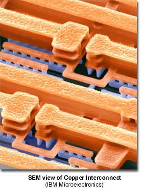
5 Copper wiring


6
7
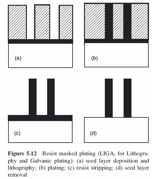
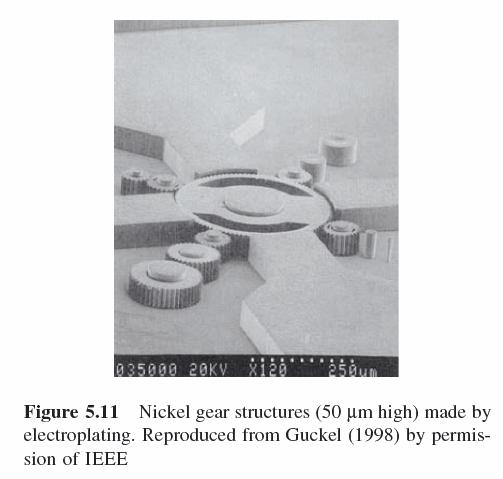
8 Lithographie, Galvanoformung, Abformung (LIGA) Fransila

9 Lithographie, Galvanoformung, Abformung (LIGA)
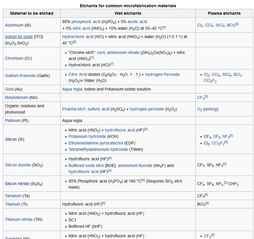
10 Etching Wet chemical etching Ion milling Reactive ion etching Chemical-Mechanical Polishing


11 Wet etching Etchant Etch stop (DI water) etching rate, anisotropy, selectivity

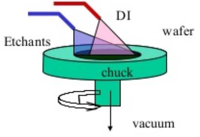
12 Wet Etching Spray etching Fransila


13 Etch rate depends on deposited m

14 Acid safety Read the MSDS Know which precautions to take Dispose of acids properly

15 Solvent safety

16 Isotropic and anisotropic etching Isotropic Anisotropic


17 KOH etching of silicon W Self limiting depth: d = W 2 KOH etches Si {110} > {100} > {111}, producing a characteristic anisotropic V-etch, with sidewalls that form a 54.7 angle with the surface (35.3 from the normal).

18 Etching through a wafer can take hours


19 KOH etching of silicon The <111> planes are etched 200 times slower than <100> planes.
 silicon.")
20 Other anisotropic etchants for silicon EDP (an aqueous solution of ethylene diamine and pyrocatechol), displays a <100>/<111> selectivity of 17X, does not etch silicon dioxide as KOH does, and also displays high selectivity between lightly doped and heavily boron-doped (ptype) silicon. Tetramethylammonium hydroxide (TMAH) presents a safer alternative than EDP, with a 37X selectivity between {100} and {111} planes in silicon.
21 HF etching of SiO 2 SiO HF = 2H + SiF H 2 O Stops at the silicon surface and leaves the surface hydrogen passivated. HF is dangerous and you require special training before using it. Larger labs have a dedicated HF station. HF reacts with glass, concrete, metals, water, oxidizers, reducers, alkalis, combustibles, organics and ceramics. It must be kept in special polyethylene or fluorocarbon plastic containers and special tools are used.

22 Etch-stop techniques p+ etch stop silicon highly doped (>10 19 cm -3 ) with boron etches very slowly Etch stop with buried masking layers implant O, N, or C to make SiO 2, SiC, or SiN x Electrochemically controlled pn etch stop The voltage drops across the reverse biased junction until the n region is exposed and then the potential at the surface oxidizes the silicon
23 Plasma etching Plasma The plasma activates the etching gas which reacts at the surface to form a gaseous product. (In PECVD a solid product is formed.)
24
25 Plasma etching The same equipment can be used for plasma etching plasma cleaning surface modification Leaves less residue than wet etching. The products are volatile.

26 Ion Milling Ions (typically Ar) are accelerated at the substrate. No chemical reaction Selectivity ~ 1:1 High vacuum Will etch anything


27 Reactive Ion Etching (RIE) Combines physical ion milling with chemical etching. Is faster and more selective than ion milling.

28 Isotropic and Anisotropic Plasma Etching Fransila You can use plasma etching to etch isotropically and anistotropically.

29 Isotropic and Anisotropic Plasma Etching Channels used for microneedles. Fransila
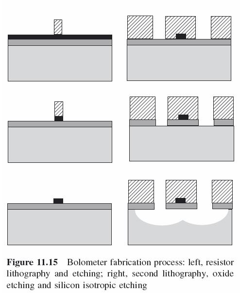
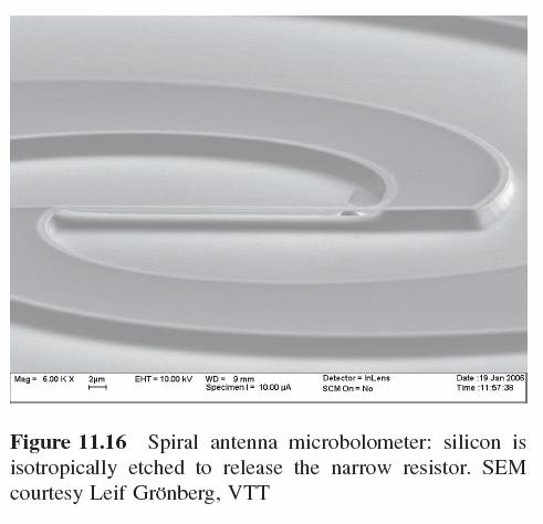
30 Microbolometer Fransila
 2.")

31 Bosch process Repeat 2 processes over and over 1. Etch Si with SF 6 (nearly isotropic) 2. Deposit passivation layer C 4 F 8 Directional etching at the bottom breaks through the passivation layer. Short cycles: smooth walls Long cycles: fast etching
 A vertical")
32 Through-Silicon Via (TSV) A vertical electrical connection (via) passing completely through a silicon wafer. Used in 3D integration.

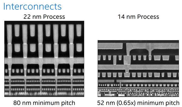
33 Chemical Mechanical Polishing (CMP)

34 Woodpile photonic crystal

35 Damascene process Inlaying of one metal in another
36


37 Cleaning Wafer cleaning is a critical function that must be repeated many times during semiconductor manufacturing. Villach/Austria is the global centre for the development and production of all single-wafer spin technology products for back- and front- end-of-line (BEOL/FEOL) cleaning, etching and stripping applications.
Czochralski Crystal Growth
 Czochralski Crystal Growth Crystal Pulling Crystal Ingots Shaping and Polishing 300 mm wafer 1 2 Advantage of larger diameter wafers Wafer area larger Chip area larger 3 4 Large-Diameter Wafer Handling
ME 189 Microsystems Design and Manufacture. Chapter 9. Micromanufacturing
 ME 189 Microsystems Design and Manufacture Chapter 9 Micromanufacturing This chapter will offer an overview of the application of the various fabrication techniques described in Chapter 8 in the manufacturing
MEMS Fabrication. Beyond Integrated Circuits. MEMS Basic Concepts
 MEMS Fabrication Beyond Integrated Circuits MEMS Basic Concepts Uses integrated circuit fabrication techniques to make mechanical as well as electrical components on a single chip. Small size 1µm 1mm Typically
Chemical Vapor Deposition
 Chemical Vapor Deposition ESS4810 Lecture Fall 2010 Introduction Chemical vapor deposition (CVD) forms thin films on the surface of a substrate by thermal decomposition and/or reaction of gas compounds
EE 330 Lecture 9. IC Fabrication Technology Part II. -Oxidation -Epitaxy -Polysilicon -Planarization -Resistance and Capacitance in Interconnects
 EE 330 Lecture 9 IC Fabrication Technology Part II -Oxidation -Epitaxy -Polysilicon -Planarization -Resistance and Capacitance in Interconnects Review from Last Time Etching Dry etch (anisotropic) SiO
Manufacturing Technologies for MEMS and SMART SENSORS
 4 Manufacturing Technologies for MEMS and SMART SENSORS Dr. H. K. Verma Distinguished Professor (EEE) Sharda University, Greater Noida (Formerly: Deputy Director and Professor of Instrumentation Indian
Chapter 3 Silicon Device Fabrication Technology
 Chapter 3 Silicon Device Fabrication Technology Over 10 15 transistors (or 100,000 for every person in the world) are manufactured every year. VLSI (Very Large Scale Integration) ULSI (Ultra Large Scale
Silicon Epitaxial CVD Want to create very sharp PN boundary grow one type layer on other in single crystal form High dopant layers on low dopant
 Silicon Epitaxial CVD Want to create very sharp PN boundary grow one type layer on other in single crystal form High dopant layers on low dopant substrate Creates latch up protection for CMOS Buried Epi
EE40 Lec 22. IC Fabrication Technology. Prof. Nathan Cheung 11/19/2009
 Suggested Reading EE40 Lec 22 IC Fabrication Technology Prof. Nathan Cheung 11/19/2009 300mm Fab Tour http://www-03.ibm.com/technology/manufacturing/technology_tour_300mm_foundry.html Overview of IC Technology
EE 5344 Introduction to MEMS. CHAPTER 3 Conventional Si Processing
 3. Conventional licon Processing Micromachining, Microfabrication. EE 5344 Introduction to MEMS CHAPTER 3 Conventional Processing Why silicon? Abundant, cheap, easy to process. licon planar Integrated
Lect. 2: Basics of Si Technology
 Unit processes Thin Film Deposition Etching Ion Implantation Photolithography Chemical Mechanical Polishing 1. Thin Film Deposition Layer of materials ranging from fractions of nanometer to several micro-meters
Metallization deposition and etching. Material mainly taken from Campbell, UCCS
 Metallization deposition and etching Material mainly taken from Campbell, UCCS Application Metallization is back-end processing Metals used are aluminum and copper Mainly involves deposition and etching,
Institute of Solid State Physics. Technische Universität Graz. Deposition. Franssila: Chapters 5 & 6. Peter Hadley
 Technische Universität Graz Institute of Solid State Physics Deposition Franssila: Chapters 5 & 6 Peter Hadley Silicon wafers Total Thickness Variation: a good 8" Prime wafer would be < 15 m Site flatness
L5: Micromachining processes 1/7 01/22/02
 97.577 L5: Micromachining processes 1/7 01/22/02 5: Micromachining technology Top-down approaches to building large (relative to an atom or even a transistor) structures. 5.1 Bulk Micromachining A bulk
Lecture 5: Micromachining
 MEMS: Fabrication Lecture 5: Micromachining Prasanna S. Gandhi Assistant Professor, Department of Mechanical Engineering, Indian Institute of Technology, Bombay, Recap: Last Class E-beam lithography X-ray
IC/MEMS Fabrication - Outline. Fabrication
 IC/MEMS Fabrication - Outline Fabrication overview Materials Wafer fabrication The Cycle: Deposition Lithography Etching Fabrication IC Fabrication Deposition Spin Casting PVD physical vapor deposition
Today s Class. Materials for MEMS
 Lecture 2: VLSI-based Fabrication for MEMS: Fundamentals Prasanna S. Gandhi Assistant Professor, Department of Mechanical Engineering, Indian Institute of Technology, Bombay, Recap: Last Class What is
Silicon Epitaxial CVD Want to create very sharp PN boundary grow one type layer on other in single crystal form High dopant layers on low dopant
 Silicon Epitaxial CVD Want to create very sharp PN boundary grow one type layer on other in single crystal form High dopant layers on low dopant substrate Creates latch up protection for CMOS Buried Epi
Semiconductor Manufacturing Process 10/11/2005
 Semiconductor Manufacturing Process 10/11/2005 Photolithography Oxidation CVD PVD Photolithography The purpose of photolithography is to imprint the desired pattern of a micro component on a substrate,
Micromachining AMT 2505
 Micromachining AMT 2505 Shanmuga Raja.B (BVB0912004) Module leader : Mr. Raja Hussain Introduction Micromachining are inherently connected to the evolution of Micro Electro Mechanical Systems (MEMS). Decades
Review of CMOS Processing Technology
 - Scaling and Integration Moore s Law Unit processes Thin Film Deposition Etching Ion Implantation Photolithography Chemical Mechanical Polishing 1. Thin Film Deposition Layer of materials ranging from
INF5490 RF MEMS. LN02: MEMS Fabrication. Spring 2012, Oddvar Søråsen Department of Informatics, UoO
 INF5490 RF MEMS LN02: MEMS Fabrication Spring 2012, Oddvar Søråsen Department of Informatics, UoO 1 Micromachining Today s lecture Important process steps General Summary: MEMS-specific steps Examples
EE 143 CMOS Process Flow
 EE 143 CMOS rocess Flow CT 84 D D G Sub G Sub S S G D S G D S + + + + - MOS Substrate Well - MOS Substrate EE 143 CMOS rocess Flow CT 85 hotoresist Si 3 4 SiO 2 Substrate selection: moderately high resistivity,
Microstructure of Electronic Materials. Amorphous materials. Single-Crystal Material. Professor N Cheung, U.C. Berkeley
 Microstructure of Electronic Materials Amorphous materials Single-Crystal Material 1 The Si Atom The Si Crystal diamond structure High-performance semiconductor devices require defect-free crystals 2 Crystallographic
Fabrication Process. Crystal Growth Doping Deposition Patterning Lithography Oxidation Ion Implementation CONCORDIA VLSI DESIGN LAB
 Fabrication Process Crystal Growth Doping Deposition Patterning Lithography Oxidation Ion Implementation 1 Fabrication- CMOS Process Starting Material Preparation 1. Produce Metallurgical Grade Silicon
There are basically two approaches for bulk micromachining of. silicon, wet and dry. Wet bulk micromachining is usually carried out
 57 Chapter 3 Fabrication of Accelerometer 3.1 Introduction There are basically two approaches for bulk micromachining of silicon, wet and dry. Wet bulk micromachining is usually carried out using anisotropic
EE C245 ME C218 Introduction to MEMS Design Fall 2011
 Lecture Outline EE C245 ME C218 Introduction to MEMS Design Fall 2011 Prof. Clark T.-C. Nguyen Dept. of Electrical Engineering & Computer Sciences University of California at Berkeley Berkeley, CA 94720
Chapter 2 OVERVIEW OF MEMS
 6 Chapter 2 OVERVIEW OF MEMS 2.1 MEMS and Microsystems The term MEMS is an abbreviation of microelectromechanical system. MEMS contains components ofsizes in 1 micrometer to 1 millimeter. The core element
Make sure the exam paper has 9 pages total (including cover page)
") UNIVERSITY OF CALIFORNIA College of Engineering Department of Electrical Engineering and Computer Sciences Fall 2010 EE143 Midterm Exam #2 Family Name First name SID Signature Solution Make sure the exam
UNIVERSITY OF CALIFORNIA College of Engineering Department of Electrical Engineering and Computer Sciences Fall 2010 EE143 Midterm Exam #2 Family Name First name SID Signature Solution Make sure the exam
EE 330 Lecture 8. IC Fabrication Technology Part II. - Oxidation - Epitaxy - Polysilicon - Interconnects
 EE 330 Lecture 8 IC Fabrication Technology Part II - Oxidation - Epitaxy - Polysilicon - Interconnects Review from Last Time MOS Transistor Bulk Source Gate Drain p-channel MOSFET Lightly-doped n-type
ECE 440 Lecture 27 : Equilibrium P-N Junctions I Class Outline:
 ECE 440 Lecture 27 : Equilibrium P-N Junctions I Class Outline: Fabrication of p-n junctions Contact Potential Things you should know when you leave Key Questions What are the necessary steps to fabricate
Isolation of elements
 1 In an IC, devices on the same substrate must be isolated from one another so that there is no current conduction between them. Isolation uses either the junction or dielectric technique or a combination
Overview. Silicon Microfabrication Part 2. Introduction to BioMEMS & Medical Microdevices
 Introduction to BioMEMS & Medical Microdevices Silicon Microfabrication Part 2 Companion lecture to the textbook: Fundamentals of BioMEMS and Medical Microdevices, by Prof., http://saliterman.umn.edu/
Silicon Microfabrication Part 2
 Introduction to BioMEMS & Medical Microdevices Silicon Microfabrication Part 2 Companion lecture to the textbook: Fundamentals of BioMEMS and Medical Microdevices, by Prof., http://saliterman.umn.edu/
Surface micromachining and Process flow part 1
 Surface micromachining and Process flow part 1 Identify the basic steps of a generic surface micromachining process Identify the critical requirements needed to create a MEMS using surface micromachining
Ion Implantation Most modern devices doped using ion implanters Ionize gas sources (single +, 2+ or 3+ ionization) Accelerate dopant ions to very
 Accelerate dopant ions to very") Ion Implantation Most modern devices doped using ion implanters Ionize gas sources (single +, 2+ or 3+ ionization) Accelerate dopant ions to very high voltages (10-600 KeV) Use analyzer to selection charge/mass
Ion Implantation Most modern devices doped using ion implanters Ionize gas sources (single +, 2+ or 3+ ionization) Accelerate dopant ions to very high voltages (10-600 KeV) Use analyzer to selection charge/mass
Mostafa Soliman, Ph.D. May 5 th 2014
 Mostafa Soliman, Ph.D. May 5 th 2014 Mostafa Soliman, Ph.D. 1 Basic MEMS Processes Front-End Processes Back-End Processes 2 Mostafa Soliman, Ph.D. Wafers Deposition Lithography Etch Chips 1- Si Substrate
INTEGRATED-CIRCUIT TECHNOLOGY
 INTEGRATED-CIRCUIT TECHNOLOGY 0. Silicon crystal growth and wafer preparation 1. Processing Steps 1.1. Photolitography 1.2. Oxidation 1.3. Layer Deposition 1.4. Etching 1.5. Diffusion 1.6 Backend: assembly,
A discussion of crystal growth, lithography, etching, doping, and device structures is presented in
 Chapter 5 PROCESSING OF DEVICES A discussion of crystal growth, lithography, etching, doping, and device structures is presented in the following overview gures. SEMICONDUCTOR DEVICE PROCESSING: AN OVERVIEW
CSCI 4974 / 6974 Hardware Reverse Engineering. Lecture 5: Fabrication processes
 CSCI 4974 / 6974 Hardware Reverse Engineering Lecture 5: Fabrication processes QUIZ 3: CMOS layout Quiz Discussion Rationale If you know how something is put together, you can figure out how to take it
The Physical Structure (NMOS)
") The Physical Structure (NMOS) Al SiO2 Field Oxide Gate oxide S n+ Polysilicon Gate Al SiO2 SiO2 D n+ L channel P Substrate Field Oxide contact Metal (S) n+ (G) L W n+ (D) Poly 1 3D Perspective 2 3 Fabrication
The Physical Structure (NMOS) Al SiO2 Field Oxide Gate oxide S n+ Polysilicon Gate Al SiO2 SiO2 D n+ L channel P Substrate Field Oxide contact Metal (S) n+ (G) L W n+ (D) Poly 1 3D Perspective 2 3 Fabrication
CMOS Technology. Flow varies with process types & company. Start with substrate selection. N-Well CMOS Twin-Well CMOS STI
 CMOS Technology Flow varies with process types & company N-Well CMOS Twin-Well CMOS STI Start with substrate selection Type: n or p Doping level, resistivity Orientation, 100, or 101, etc Other parameters
MICROCHIP MANUFACTURING by S. Wolf
 MICROCHIP MANUFACTURING by S. Wolf Chapter 22 DRY-ETCHING for ULSI APPLICATIONS 2004 by LATTICE PRESS CHAPTER 22 - CONTENTS Types of Dry-Etching Processes The Physics & Chemistry of Plasma-Etching Etching
Etching Etching Definitions Isotropic Etching: same in all direction Anisotropic Etching: direction sensitive Selectivity: etch rate difference
 Etching Etching Definitions Isotropic Etching: same in all direction Anisotropic Etching: direction sensitive Selectivity: etch rate difference between 2 materials Need strong selectivity from masking
Fabrication Technology, Part II
 EEL5225: Principles of MEMS Transducers (Fall 2003) Fabrication Technology, Part II Agenda: Process Examples TI Micromirror fabrication process SCREAM CMOS-MEMS processes Wafer Bonding LIGA Reading: Senturia,
3D technologies for integration of MEMS
 3D technologies for integration of MEMS, Fraunhofer Institute for Electronic Nano Systems Folie 1 Outlook Introduction 3D Processes Process integration Characterization Sample Applications Conclusion Folie
EECS130 Integrated Circuit Devices
 EECS130 Integrated Circuit Devices Professor Ali Javey 9/13/2007 Fabrication Technology Lecture 1 Silicon Device Fabrication Technology Over 10 15 transistors (or 100,000 for every person in the world)
3. Photolithography, patterning and doping techniques. KNU Seminar Course 2015 Robert Mroczyński
 3. Photolithography, patterning and doping techniques KNU Seminar Course 2015 Robert Mroczyński Critical technology processes Photolithography The aim of this process is to transfer (in the most accurate
EE C245 ME C218 Introduction to MEMS Design Fall 2010
 Lecture Outline EE C245 ME C218 Introduction to MEMS Design Fall 2010 Prof. Clark T.-C. Nguyen Dept. of Electrical Engineering & Computer Sciences University of California at Berkeley Berkeley, CA 94720
Midterm evaluations. Nov. 9, J/3.155J 1
 Midterm evaluations What learning activities were found most helpful Example problems, case studies (5); graphs (good for extracting useful info) (4); Good interaction (2); Good lecture notes, slides (2);
Lecture #18 Fabrication OUTLINE
 Transistors on a Chip Lecture #18 Fabrication OUTLINE IC Fabrication Technology Introduction the task at hand Doping Oxidation Thin-film deposition Lithography Etch Lithography trends Plasma processing
Introduction to CMOS VLSI Design. Layout, Fabrication, and Elementary Logic Design
 Introduction to CMOS VLSI Design Layout, Fabrication, and Elementary Logic Design CMOS Fabrication CMOS transistors are fabricated on silicon wafer Lithography process similar to printing press On each
The Berkeley Marvell NanoLab
 The History The Berkeley Marvell NanoLab The Culture The Present The BNLA The Capabilities The End MEMS Industry Group M2M 20May2014 Bill Flounders, Ph.D. NanoLabExecutive Director The History The Berkeley
ELEC 3908, Physical Electronics, Lecture 4. Basic Integrated Circuit Processing
 ELEC 3908, Physical Electronics, Lecture 4 Basic Integrated Circuit Processing Lecture Outline Details of the physical structure of devices will be very important in developing models for electrical behavior
5.8 Diaphragm Uniaxial Optical Accelerometer
 5.8 Diaphragm Uniaxial Optical Accelerometer Optical accelerometers are based on the BESOI (Bond and Etch back Silicon On Insulator) wafers, supplied by Shin-Etsu with (100) orientation, 4 diameter and
Process Flow in Cross Sections
 Process Flow in Cross Sections Process (simplified) 0. Clean wafer in nasty acids (HF, HNO 3, H 2 SO 4,...) --> wear gloves! 1. Grow 500 nm of SiO 2 (by putting the wafer in a furnace with O 2 2. Coat
VLSI Technology. By: Ajay Kumar Gautam
 By: Ajay Kumar Gautam Introduction to VLSI Technology, Crystal Growth, Oxidation, Epitaxial Process, Diffusion Process, Ion Implantation, Lithography, Etching, Metallization, VLSI Process Integration,
Most semiconductor devices contain at least one junction between p-type and n-type material. These p-n junctions are fundamental to the performance
 Ch. 5: p-n Junction Most semiconductor devices contain at least one junction between p-type and n-type material. These p-n junctions are fundamental to the performance of functions such as rectification,
Chapter 3 CMOS processing technology
 Chapter 3 CMOS processing technology (How to make a CMOS?) Si + impurity acceptors(p-type) donors (n-type) p-type + n-type => pn junction (I-V) 3.1.1 (Wafer) Wafer = A disk of silicon (0.25 mm - 1 mm thick),
Fabrication Technology, Part I
 EEL5225: Principles of MEMS Transducers (Fall 2003) Fabrication Technology, Part I Agenda: Oxidation, layer deposition (last lecture) Lithography Pattern Transfer (etching) Impurity Doping Reading: Senturia,
UT Austin, ECE Department VLSI Design 2. CMOS Fabrication, Layout Rules
 2. CMOS Fabrication, Layout, Design Rules Last module: Introduction to the course How a transistor works CMOS transistors This module: CMOS Fabrication Design Rules CMOS Fabrication CMOS transistors are
Tapered Walls Via Holes Manufactured Using DRIE Variable Isotropy Process
 Tapered Walls Via Holes Manufactured Using DRIE Variable Isotropy Process D. VASILACHE, S. RONCHIN, S. COLPO, B. MARGESIN, F. GIACOMOZZI, S. GENNARO FBK-irst, via Sommarive 18-38123 Trento, Italy; Tel.:
An optimization study on the anisotropic TMAH wet etching of silicon (100)
") International Journal of Material Science Innovations (IJMSI) 1 (3): 115-123, 2013 ISSN: 2289-4063 Academic Research Online Publisher Research Article An optimization study on the anisotropic TMAH wet
International Journal of Material Science Innovations (IJMSI) 1 (3): 115-123, 2013 ISSN: 2289-4063 Academic Research Online Publisher Research Article An optimization study on the anisotropic TMAH wet
EE 330 Lecture 12. Devices in Semiconductor Processes
 EE 330 Lecture 12 Devices in Semiconductor Processes Review from Lecture 9 Copper Interconnects Limitations of Aluminum Interconnects Electromigration Conductivity not real high Relevant Key Properties
PHYS 534 (Fall 2008) Process Integration OUTLINE. Examples of PROCESS FLOW SEQUENCES. >Surface-Micromachined Beam
 Process Integration OUTLINE. Examples of PROCESS FLOW SEQUENCES. >Surface-Micromachined Beam") PHYS 534 (Fall 2008) Process Integration Srikar Vengallatore, McGill University 1 OUTLINE Examples of PROCESS FLOW SEQUENCES >Semiconductor diode >Surface-Micromachined Beam Critical Issues in Process
PHYS 534 (Fall 2008) Process Integration Srikar Vengallatore, McGill University 1 OUTLINE Examples of PROCESS FLOW SEQUENCES >Semiconductor diode >Surface-Micromachined Beam Critical Issues in Process
Nonplanar Metallization. Planar Metallization. Professor N Cheung, U.C. Berkeley
 Nonplanar Metallization Planar Metallization Passivation Metal 5 (copper) Metal 3 (copper) Interlevel dielectric (ILD) Via (tungsten) Metal 1 (copper) Tungsten Plug to Si Silicon Caps and Plugs oxide oxide
Nanoelectronics Fabrication Facility
 Nanoelectronics Fabrication Facility Contents Introduction 2 Mask Making Module 4 Photolithography Module 6 Wet Etching and CMP Module 8 Dry Etching and Sputtering Module 10 Thermal Process and Implantation
Semiconductor Technology
 Semiconductor Technology von A bis Z Metallization www.halbleiter.org Contents Contents List of Figures List of Tables II III 1 Metallization 1 1.1 Requirements on metallization........................
CMOS Fabrication. Dr. Bassam Jamil. Adopted from slides of the textbook
 CMOS Fabrication Dr. Bassam Jamil Adopted from slides of the textbook CMOS Fabrication CMOS transistors are fabricated on silicon wafer Lithography process similar to printing press On each step, different
Wafer (1A) Young Won Lim 4/30/13
 Young Won Lim 4/30/13") Copyright (c) 2011-2013 Young W. Lim. Permission is granted to copy, distribute and/or modify this document under the terms of the GNU Free Documentation License, Version 1.2 or any later version published
Copyright (c) 2011-2013 Young W. Lim. Permission is granted to copy, distribute and/or modify this document under the terms of the GNU Free Documentation License, Version 1.2 or any later version published
Activities in Plasma Process Technology at SENTECH Instruments GmbH, Berlin. Dr. Frank Schmidt
 Activities in Plasma Process Technology at SENTECH Instruments GmbH, Berlin Dr. Frank Schmidt The Company Company Private company, founded 1990 80 employees ISO 9001 Location Science & Technology Park,
Lecture 22: Integrated circuit fabrication
 Lecture 22: Integrated circuit fabrication Contents 1 Introduction 1 2 Layering 4 3 Patterning 7 4 Doping 8 4.1 Thermal diffusion......................... 10 4.2 Ion implantation.........................
Examples of dry etching and plasma deposition at Glasgow University
 Examples of dry etching and plasma deposition at Glasgow University Glasgow has pioneered and established many novel research activities involving the development of new dry etch processes and dry etch
Doping and Oxidation
 Technische Universität Graz Institute of Solid State Physics Doping and Oxidation Franssila: Chapters 13,14, 15 Peter Hadley Technische Universität Graz Institute of Solid State Physics Doping Add donors
Semiconductor device fabrication
 REVIEW Semiconductor device fabrication is the process used to create the integrated circuits (silicon chips) that are present in everyday electrical and electronic devices. It is a multiplestep sequence
EE 330 Lecture 9. IC Fabrication Technology Part 2
 EE 330 Lecture 9 IC Fabrication Technology Part 2 Quiz 8 A 2m silicon crystal is cut into wafers using a wire saw. If the wire diameter is 220um and the wafer thickness is 350um, how many wafers will this
Solid State Sensors. Microfabrication 8/22/08 and 8/25/08
 Solid State Sensors Microfabrication 8/22/08 and 8/25/08 Purpose of This Material To introduce the student to microfabrication techniques as used to fabricate MEMS Sensors Understand concepts not specifics
ECE321 Electronics I
 ECE321 Electronics I Lecture 19: CMOS Fabrication Payman Zarkesh-Ha Office: ECE Bldg. 230B Office hours: Tuesday 2:00-3:00PM or by appointment E-mail: payman@ece.unm.edu Slide: 1 Miller Effect Interconnect
Supporting Information: Model Based Design of a Microfluidic. Mixer Driven by Induced Charge Electroosmosis
 Supporting Information: Model Based Design of a Microfluidic Mixer Driven by Induced Charge Electroosmosis Cindy K. Harnett, Yehya M. Senousy, Katherine A. Dunphy-Guzman #, Jeremy Templeton * and Michael
Ion Implantation Most modern devices doped using ion implanters Implant dopants by accelerating individual atoms (ions) Ionize gas sources (single +,
 Ionize gas sources (single +,") Ion Implantation Most modern devices doped using ion implanters Implant dopants by accelerating individual atoms (ions) Ionize gas sources (single +, 2+ or 3+ ionization) Use analyzer to selection charge/mass
Ion Implantation Most modern devices doped using ion implanters Implant dopants by accelerating individual atoms (ions) Ionize gas sources (single +, 2+ or 3+ ionization) Use analyzer to selection charge/mass
Microelectronics. Integrated circuits. Introduction to the IC technology M.Rencz 11 September, Expected decrease in line width
 Microelectronics Introduction to the IC technology M.Rencz 11 September, 2002 9/16/02 1/37 Integrated circuits Development is controlled by the roadmaps. Self-fulfilling predictions for the tendencies
1.1 Background Cu Dual Damascene Process and Cu-CMP
 Chapter I Introduction 1.1 Background 1.1.1 Cu Dual Damascene Process and Cu-CMP In semiconductor manufacturing, we always directed toward adding device speed and circuit function. Traditionally, we focused
Overview of Dual Damascene Cu/Low-k Interconnect
 ERC Retreat Stanford: New Chemistries & Tools for scco 2 Processing of Thin Films Overview of Dual Damascene Cu/Low-k Interconnect P. Josh Wolf 1,4 - Program Manager, Interconnect Div. josh.wolf@sematech.org
Lecture 2: CMOS Fabrication Mark McDermott Electrical and Computer Engineering The University of Texas at Austin
 Lecture 2: CMOS Fabrication Mark McDermott Electrical and Computer Engineering The University of Texas at Austin Agenda Last module: Introduction to the course How a transistor works CMOS transistors This
Semiconductor Technology
 Semiconductor Technology from A to Z Oxidation www.halbleiter.org Contents Contents List of Figures List of Tables II III 1 Oxidation 1 1.1 Overview..................................... 1 1.1.1 Application...............................
Figure 2.3 (cont., p. 60) (e) Block diagram of Pentium 4 processor with 42 million transistors (2000). [Courtesy Intel Corporation.
 (e) Block diagram of Pentium 4 processor with 42 million transistors (2000). [Courtesy Intel Corporation.") Figure 2.1 (p. 58) Basic fabrication steps in the silicon planar process: (a) oxide formation, (b) selective oxide removal, (c) deposition of dopant atoms on wafer, (d) diffusion of dopant atoms into exposed
Figure 2.1 (p. 58) Basic fabrication steps in the silicon planar process: (a) oxide formation, (b) selective oxide removal, (c) deposition of dopant atoms on wafer, (d) diffusion of dopant atoms into exposed
A High Speed Surface Illuminated Si Photodiode. Using Microstructured Holes for Absorption. Enhancements at nm wavelength
 A High Speed Surface Illuminated Si Photodiode Using Microstructured Holes for Absorption Enhancements at 900 1000 nm wavelength Supporting Information Yang Gao, Hilal Cansizoglu, Soroush Ghandiparsi,
Mikrosensorer. Microfabrication 1
 Mikrosensorer Microfabrication 1 Literature Introductory MEMS Fabrication and Applications Thomas M. Adams and Richard A. Layton Available as ebook on http://www.lub.lu.se/en/search/lubsearch.html This
Copper Interconnect Technology
 Tapan Gupta Copper Interconnect Technology i Springer Contents 1 Introduction 1 1.1 Trends and Challenges 2 1.2 Physical Limits and Search for New Materials 5 1.3 Challenges 6 1.4 Choice of Materials 7
Chapter 4. UEEP2613 Microelectronic Fabrication. Oxidation
 Chapter 4 UEEP2613 Microelectronic Fabrication Oxidation Prepared by Dr. Lim Soo King 24 Jun 2012 Chapter 4...113 Oxidation...113 4.0 Introduction... 113 4.1 Chemistry of Silicon Dioxide Formation... 115
Lecture 10. Metallization / Back-end technology (BEOL)
") Lecture 10 Metallization / Back-end technology (BEOL) Lecture 9: Metallization and BEOL Metallization Technology Evaporation Sputtering Back End Of the Line (BEOL) ITRS Requirements Evolution of Metallization
Lecture 10 Metallization / Back-end technology (BEOL) Lecture 9: Metallization and BEOL Metallization Technology Evaporation Sputtering Back End Of the Line (BEOL) ITRS Requirements Evolution of Metallization
Metallizing High Aspect Ratio TSVs For MEMS Challenges and Capabilities. Vincent Mevellec, PhD
 Metallizing High Aspect Ratio TSVs For MEMS Challenges and Capabilities Vincent Mevellec, PhD Agenda Introduction MEMS and sensors market TSV integration schemes Process flows for TSV Metallization aveni
IC Fabrication Technology Part III Devices in Semiconductor Processes
 EE 330 Lecture 10 IC Fabrication Technology Part III Metalization and Interconnects Parasitic Capacitances Back-end Processes Devices in Semiconductor Processes Resistors Diodes Review from Last Lecture
ENG/PHYS3320 Microsystems Technology Chapter 2 Fabrication of Microsystems
 ENG/PHYS3320 Microsystems Technology Chapter 2 Fabrication of Microsystems ENG/PHYS3320: R.I. Hornsey Fab: 1 Fabrication Many of the new transducers are based on a technology known as micromachining a
Complementary Metal Oxide Semiconductor (CMOS)
") Technische Universität Graz Institute of Solid State Physics Complementary Metal Oxide Semiconductor (CMOS) Franssila: Chapters 26,28 Technische Universität Graz Institute of Solid State Physics Complementary
Technische Universität Graz Institute of Solid State Physics Complementary Metal Oxide Semiconductor (CMOS) Franssila: Chapters 26,28 Technische Universität Graz Institute of Solid State Physics Complementary
Interconnects OUTLINE
 Interconnects 1 Interconnects OUTLINE 1. Overview of Metallization 2. Introduction to Deposition Methods 3. Interconnect Technology 4. Contact Technology 5. Refractory Metals and their Silicides Reading:
EE CMOS TECHNOLOGY- Chapter 2 in the Text
 1 EE 212 FALL 1999-00 CMOS TECHOLOGY- Chapter 2 in the Text In this set of notes we will describe a modern CMOS process flow. In the simplest CMOS technologies, we need to realize simply MOS and MOS transistors
3. Overview of Microfabrication Techniques
 3. Overview of Microfabrication Techniques The Si revolution First Transistor Bell Labs (1947) Si integrated circuits Texas Instruments (~1960) Modern ICs More? Check out: http://www.pbs.org/transistor/background1/events/miraclemo.html
Chapter 4 : ULSI Process Integration (0.18 m CMOS Process)
") Chapter : ULSI Process Integration (0.8 m CMOS Process) Reference. Semiconductor Manufacturing Technology : Michael Quirk and Julian Serda (00). - (00). Semiconductor Physics and Devices- Basic Principles(/e)
Chapter : ULSI Process Integration (0.8 m CMOS Process) Reference. Semiconductor Manufacturing Technology : Michael Quirk and Julian Serda (00). - (00). Semiconductor Physics and Devices- Basic Principles(/e)
1 MARCH 2017 FILM DEPOSITION NANOTECHNOLOGY
 1 MARCH 2017 FILM DEPOSITION NANOTECHNOLOGY PRESENTATION Pedro C. Feijoo E-mail: PedroCarlos.Feijoo@uab.cat FABRICATION TECHNOLOGIES FOR NANOELECTRONIC DEVICES. PEDRO C. FEIJOO 2 FILM GROWTH Chemical vapor