In Situ Investigations of Solid Electrolyte Interphase Formation and Properties in Lithium Ion Batteries
|
|
|
- Damon Doyle
- 6 years ago
- Views:
Transcription
1 In Situ Investigations of Solid Electrolyte Interphase Formation and Properties in Lithium Ion Batteries by Anton V. Tokranov B.S. Materials Science and Engineering, Johns Hopkins University, 2009 A dissertation submitted in partial fulfillment of the requirements for the Degree of Doctor of Philosophy in the School of Engineering at Brown University Providence, Rhode Island May, 2015
2 Copyright 2015 by Anton V. Tokranov ii
3 This dissertation by Anton V. Tokranov is accepted in its present form by the School of Engineering as satisfying the dissertation requirement for the degree of Doctor of Philosophy Date (Professor Brian W. Sheldon), Advisor Recommended to the Graduate Council Date (Professor Eric Chason), Reader Date (Professor Huajian Gao), Reader Approved by the Graduate Council Date (Professor Peter M. Weber) Dean of the Graduate School iii
4 Curriculum Vitae Anton V. Tokranov was born on December 19 th 1988 in Leningrad, USSR (which became St. Petersburg, Russian Federation shortly after birth). After 6 th grade Anton moved with his parents to United States, and in 2006 he graduate from Shaker High School, in New York state. He was accepted to Johns Hopkins University (Baltimore, MD) where Anton majored in Materials Science. At the end of his sophomore year (2008) he was able to do a summer REU at Carnegie Mellon University. During junior year Anton started doing research on Nanoporous metals, and was able to graduate with honors in 3 years. In 2009, he was awarded a fellowship to pursue Ph.D. degree in Engineering at Brown University, Providence, RI. Anton accepted the position and started his research on July During his time he has had a productive collaboration with General Motors Corporation which resulting in several publications, and the first 1 st author paper published in 2013, titled: The Origin of Stress in the Solid Electrolyte Interphase on Carbon Electrodes for Li Ion Batteries. The subsequent work also included Burker Corporation and resulted in the work titled: In Situ Atomic Force Microscopy Study of Initial Solid Electrolyte Interphase Formation on Silicon Electrodes for Li-Ion Batteries. iv
5 Acknowledgements Firstly, I would like to acknowledge my advisor Professor Brian W. Sheldon who guided me through this dissertation. With his help and direction I was able to organize my thoughts in a coherent manner. This was imperative since I have a tendency to get distracted with experiments: the size of the appendices is evidence of this. It was a great honor and a pleasure to conduct work under his supervision. I would also like to express my gratitude to my thesis readers, Professor Eric Chason and Professor Huajian Gao, for their time, patience and instructive suggestions that have contributed substantially to this thesis. I would also like to acknowledge my collaborators. First, I would like to thank Dr. Xingcheng Xiao at General Motors for his advice and suggestions: it was with his support that this project got started. I would also like to thank Dr. Chunzeng Li and Dr. Stephen Minne from Bruker for allowing me to test their in situ AFM setup. This hugely advanced my work. Additionally I want to express my gratitude to Dr. Amartya Mukhopadhyay, who worked with me when he was a post-doc at Brown and continued our collaboration when he became a professor. I am also grateful to the administrative assistants and technical staff within the School of Engineering at Brown University for their invaluable assistance. Most notably: Anthony McCormick for keeping FIB and TEMs working, Michael Jibitsky for keeping the cleanroom running well, Charles Vickers for making all the parts I drew up, Brian Corkum and Paul Waltz for helping me whenever I decide to break something in lab, and Diane Felber and Peggy Mercurio for all the administrative work I made them do. v
6 I want to thank members of Professor Sheldon s lab. They were always there to help me out whether I needed to run my idea s by them, or help with something in lab, as long as it wasn t cleaning the lab. This includes Aaron Kessman, Amartya Mukhopadhya, Dawei Lui, Yang Lei, Xin Su, Sumit Kumar Soni, Jay Sheth, Ravi Kumar, Leah Nation, Sugeetha Vasudevan, Susan Herringer, Will Ellis, and Kevin Sena. Additionally I would like to thank Professor Robert Hurt and Fei Guo for their help and collaboration on the carbon work. I also want to thank all my friends for helping me through this and still being my friend when I disappeared for a bit. Special thanks goes to Don Ho for being a great roommate, and Aruna Sigdel for being a great replacement roommate. Dan Corbi and Sarah Schrier who still managed to stay in touch after college. To the climbing group that kept changing members, but never died out, including Ravi Kumar, Naubahar Agha, Daniel Gerbig, Sebastjan Glinsek, Melissa Holzhauer, Chris Geggie, and the previously mentioned Don Ho. And to all my friends I tortured with long bike rides and hikes, including the ones listed above with the addition of Jay Sheth, whom I could never get into climbing. Lastly Brown cycling for getting me started in racing. Thanks Guys! Finally, I thank my parents for setting me on this path, and giving me advice, including some technical (I guess there are upsides to having two parents with PhDs.). Lastly I want to thank my loving and supportive girlfriend Andrea Weber, who has now put up with me for almost 4 years. More importantly is that she is still putting up with me as I am writing this at a completely reasonable hour, love you! Thank you everyone! vi
7 This work is dedicated to my parents Dr. Vadim Tokranov & Dr. Natalya Tokranova vii
8 Table of Contents Signature Page Curriculum Vitae Acknowledgments Table of Content List of Tables List of Figures Abstract iii iv v viii xii xiii xix 1. INTRODUCTION Lithium Ion Battery Background Lithium Ion Battery Operation Solid Electrolyte Interphase SEI Formation Thesis Organization References INITIAL EXPERIMENTS ON STRESS IN GRAPHITIC CARBON DURING CYCLING Introduction Experimental Details Results Development of well-ordered graphitic thin films...13 viii
9 Electrochemical behavior of the CVD C films In-situ stress determination during galvanostatic cycling Discussion Conclusion References THE ORIGIN OF STRESS IN THE SOLID ELECTROLYTE INTERPHASE ON CARBON ELECTRODES FOR LI ION BATTERIES Introduction Experimental Methods Near-Surface Processes During the First Cycle Irreversible stress evolution Near surface characterization Impact of ALD aluminum oxide coatings Interpretation Impact of Cycling Conditions First cycle variations Later cycles and passivation of the surface Discussion and Conclusions References IN SITU ATOMIC FORCE MICROSCOPY STUDY OF INITIAL SOLID ELECTROLYTE INTERPHASE FORMATION ON SILICON ELECTRODES FOR LI-ION BATTERIES Introduction Experimental Approach.. 54 ix
10 4.3. Results Expansion and contraction of Si Islands SEI on copper Simultaneous SEI formation and silicon expansion Silicon coated with aluminum oxide Surface roughness Impact of initial cycling conditions Analysis and Discussion SEI formation SEI thickness and stability Conclusions References Evolution of Solid Electrolyte Interphase on Silicon in the Intermediate Time Range Introduction Experimental Setup Results SEI growth, structure and deformation Interfacial phenomena Analysis and Discussion Mathematical model of SEI formation Comparisons with EIS data Implications for the mechanical response of the SEI Conclusions 137 x
11 5.6. References Conclusions & Future Directions Conclusions Future Directions References APPENDICES: A. ADDITIONAL CARBON EXPERIMENTS A.1. Updated CVD Growth and Characterization A.2. VAGLA Graphitization Experiments A.3. Impact of PC on CVD Carbon Structure A.4. Carbon Films with Modified PITT Analysis A.5. Self-Discharge Experiments A.6. References B. ADDITIONAL SILICON EXPERIMENTS B.1. Si Electrodes with FEC Electrolyte Additive B.2. Anomalous Silicon Stress Response During Voltage Holds B.3. Initial Si SEI Experiments B.4. References 198 xi
12 List of Tables Table 3.1 Capacity and Stress observed in a CVD carbon thin film during constant voltage holds; in the order of occurrence (holds showing delithiation are highlighted). 29 Table 4.1 Surface roughness of Cu and Si during cycling...71 Table 5.1 Sequence of SEI formation Table 5.2 Some possible values of ( = 10 GPa, and xii
13 List of Figures Figure 2.1 Figure 2.2 Figure 2.3 Figure 3.1 Figure 3.2 Figure 3.3 Figure 3.4 Figure 3.5 Figure 3.6 Schematic representation of the electrochemical cell (a) TEM image, obtained with cross-sectional sample (b) SEM image of the CVD C film..14 (a) Magnified view (between 0.4 V and 0 V) of Potential vs. Capacity plot recorded during galvanostatic cycling of CVD C against Li metal, C/20 rate. (b) Combined Potential and Nominal Stress (stress at the beginning of cycle set to 0) plots recorded during galvanostatic cycling at different rates (currents) corresponding to C/20; C/10 and C/5 rates Stress response of the CVD Carbon thin film to voltage holds during the first cycle. The stress due to SEI formation is initially visible at 0.6V, with increase in magnitude at 0.1V when significant lithiation of the electrode starts...28 Stress data for the first cycle of the carbon films highlighting the difference the ALD of alumina makes. The cycle is more reversible, showing less residual stress, and the slope during the 0.4V is also almost flat for the sample with a surface film...31 Cross-section TEM of the surface region, obtained with (a) CVD Carbon sample after one cycle, showing the amorphization of the near surface region. The graphitic carbon structure was confirmed with microdiffraction, in contrast to the near surface region which is amorphous. A porous layer approximately 5 nm thick is observed at the surface. (b) CVD Carbon sample with 2.2nm of Alumina deposited on the surface. The amorphous layer is thinner than that of the sample without the surface coating shown in part (a). A porous surface of approximately 3nm is also observed. (c) An untreated CVD Carbon sample before cycling, showing a clean carbon surface XPS depth profiles obtained with (a) an untreated carbon film after 1 cycle, the data shows a high carbon content near the surface which tends to increase with the time or depth. By contrast, Lithium and Fluorine decrease with depth. (b) A carbon film with amorphous Alumnia coating (via ALD) after 1 cycle. Carbon content was lower than that on the film without alumina coating and increased with the sputter time / depth. Unlike carbon, Lithium and Fluorine peaked in the near surface region and decreased with depth. (c) Al depth profile shows that the surface region is rich in aluminum, which is consistent with a surface coating TOF SIMS depth profiles for cycled films. The Y-axis is the normalized intensity which shows number of each ion relative to the total ions recorded (some ions were in very low intensity and a multiply factor has been applied to show data on the graph, as noted in the legend), and X-axis is the calculated sputter depth calibrated with the sputter rate on SiO 2. (a) Untreated CVD carbon film after 1 cycle. The data shows the C 2 - ion concentration increasing with depth, with Li 2 F + showing the opposite trend. Li 2 O + ions are from Li 2 O and CH 3 + ions are from the organic component of the SEI. (b) CVD carbon film with 2.2nm ALD of alumina coating after 1 cycle. The data shows similar trends as the sample in part (a) with 2 major differences: first there is evidence of a surface layer with higher Li 2 F - content, second the surface region is rich in aluminum, which is consistent with a surface coating (a) CVD Carbon film stress compared to Cu and Au stress, (b) detailed version of Cu and Au stress data. The potential was first stabilized at 1.5V (relative to Li/Li + ), then dropped to xiii
14 0.5V for 5 hour, and then returned to 1.5V. The stress response for carbon is irreversible, and more than an order of magnitude larger compared to the metal current collectors Figure 3.7 Stress in a CVD Carbon film during a longer hold at 0.5V, showing that the process is not terminated at longer time Figure 3.8 TOF SIMS depth profiles for cycled films, where the 0.5V hold length was varied. The Y- axis is the normalized intensity which shows number of each ion relative to the total ions recorded (some ions had very low intensity and a multiplication factor was applied, as noted in the legend). The X-axis is the calculated sputter depth calibrated with the sputter rate on SiO 2. (a) CVD carbon sample with a 10 hour hold and no further cycling. (b) CVD carbon sample with a 24 hour hold and 2 further cycles, including a 10hr hold at 1mV. Both samples show increasing graphitic carbon content consistent with previous experiments in Figure 4, but the sample shown in (b) has evidence of a surface layer similar to that of the sample with the ALD alumina coating Figure 3.9 Figure 3.10 Effect of electrolyte on the initial surface processes. Both electrolytes show significant irreversible stress during the hold Stress response of carbon during later holds. The irreversible stress seen during the first hold disappears in later holds, after the sample has completed a full cycle...40 Figure 3.11 Relationship between stress data and the electrochemical cycling data for the electrodes, during the 0.5V holds shown in Figure 10. The first two holds (red) were done before cycling to lower potentials, while the remaining three (blue) were done after full cycles. (a) Stress vs. capacity. (b) Stress change vs. current Figure 3.12 Figure 3.13 Figure 4.1 Figure 4.2 Figure 4.3 Figure 4.4 Figure 4.5 Proposed mechanism: (a) Carbon electrode before cycling, (b) surface disruption caused by solvated ions in the first cycle, (c) surface disruption increases amorphization, (d) inorganic SEI forms on the surface preventing further damage to the graphite (e) stable inorganic layer thickness is reached Proposed model: amorphous layer acts as an intermediate between graphitic material and inorganic SEI, which softens the impact of carbon expansion during cycling on an inflexible surface later Si island after cycling to (a) 0.2 V, (b) 2.2 V, (c) 0.1 V, (d) 2.2 V. In (a) and (b) the SEI is stable, but is unable to withstand electrode expansion in (c) and shows irreversible SEI in (d) Schematic showing our interpretation of the results in Figure (a) Configuration for Cu SEI measurements, original island height is approximately 55 nm, (b) After SEI growth the height difference decreases, and is measured (c) SEI thickness on Cu measured by AFM (Orignal Height Current Height). Error bars show the average deviation..61 3D image of electrode with the pulse SEI (a) pristine electrode, (b) fully lithiated electrode during the 2 nd cycle Height of Si electrode (error bars in (a) and (b) show the average deviation): (a) in situ AFM measurements during the slower first cycle, showing thick SEI formation; (b) in situ AFM measurements during faster first cycle...65 xiv
15 Figure 4.6 Height of Si electrode (a) post mortem TEM image after same cycling schedule as in figure 4.5(a), (b) EDS of the cross-section (graph represents the intensity of elements along the line shown on the right) Figure 4.7 Figure 4.8 Figure 4.9 Figure 4.10 Figure 4.11 Figure 5.1 Figure 5.2 Figure 5.3 Figure 5.4 Figure 5.5 Figure 5.6 Figure 5.7 Al 2 O 3 coated sample: (a) 2D image of the first cycle showing front motion (the front is surrounded by the green outline), (b) 3D image during the first cycle showing the front motion (the front is surrounded by the green outline), (c) 3D image of the Si during the second cycle (the area where the transformation was first seen in the first cycle is surrounded by the blue outline), (d) thickness plot, (e) front progress relative to the edge, multiple heights are shown to highlight the rapid transformation that is occurring Change in electrode height due to various processes: (a)-(b) SEI diffusion during a fast lithiation (1.5 V 50 mv voltage drop). (a) Electrode total height (Si + SEI height), (b) The expansion of the electrode relative to the electrodes original height (1 st cycle irreversible expansion included). (c) SEI growth during 0.6 V holds. It can be seen that the SEI does not grow significantly on Cu surface (after initial rapid formation) or after being exposed to a lower potentials. Data smoothing used for electrode with thick SEI, due to surface roughness...74 SEI growth model: (a) Formation of organic decomposition products at higher potential. (b) continuing decomposition increases the SEI thickness and decreases mesoporosity, which reduces the growth rate as the solvation complex now has to diffuse to the electrode through SEI that is thicker and denser. (c) At lower voltage a dense SEI forms, which allows Li-ion diffusion but passivates by limiting both electrolyte diffusion and electrical conductivity...75 Configurational differences between thin film and particle electrodes SEI failure limit based on SEI thickness, h, and estimated properties SEI growth model: (a) SEI decomposition at higher potential, resulting in organic products. (b) continuing decomposition increases the SEI thickness and decreases mesoporosity, which reduces the growth rate as the solvation complex now has to diffuse to the electrode through SEI that is thicker and denser (ultimately larger complexes are unable to reach the surface at all). (c) At lower voltage a dense SEI forms, which allows Li-ion diffusion and passivates by limiting electrical conductivity (a) SEI growth observations. Deformation of the surface material (b) slow cycling, (c) pulse cycling. You can clearly see two distinct regions in the plot show slower cycling. The large scattering is likely due to organic material sticking to the tip. 107 EIS data. Resistance during a voltage hold in the 1 st cycle: (a) 0.6V, (b) 0.05V. Later cycles data: (c) Resistance and Conductivity, R values represented by solid points, Conductivity by hollow points (a) PITT fit of the AFM data, (b) PITT fit results for the AFM lithiation (a) PITT Data summary for a sample with thick SEI showing diffusion values. (b) Summary of current exchange density, for a sample with slow cycling. (c) Pulse slow comparison in coin cells during the 4 th cycle SEI growth observations during the first cycle at 0.6V. With the fit to the model proposed in previous chapter (a) Schematic for the SEI growth model. (b) Schematic for the Li Flux Model xv
16 Figure 5.8 Figure 5.9 (a) Intial fit of SEI resistance to the model proposed in section 5.4.2, (b) improved fit with surface roughness accounted for (a) Model for the SEI growth with a slow first cycle. Initial SEI is mesoporous organic material, which only forms in the first cycle. In the following cycles inorganic SEI is formed at lower potential, filling in the pore space. (b) Alternatively faster pulse cycling prevents formation of organic SEI in the first cycle 129 Figure 5.10 and as a function of f ( = 0.025, 0.05, and 0.1, p=1.5) 136 Figure 5.11 vs. with varying p values (a phenomenological measure of tortuosity, 1 is consistent with straight pores, 1.5 assumes monodisperse insulating spherical particles extending the diffusion path, and is commonly used for battery electrodes). 136 Figure A.1 Figure A.2 Figure A.3 Figure A.4 Figure A.5 Figure A.6 Figure A.7 Figure A.8 Figure A.9 Optical images of sequential CVD samples. Dark areas are carbon rich, while light areas are carbon poor. The corresponding Raman spectra can be seen in Figure A RAMAN spectra of sequential CVD samples. Two scans of each sample were taken: light and dark areas or alternatively two random spots if the surface was even, as well as 100 μm x 100 μm area average, and 10x10 points FIB cross section of CVD C film showing nickel roughening (a) Growth stress data, (b) Raman comparison of area average spectra, (c) Zoom in on between 1300 and 1700 cm Cycling and stress data during the first cycle for samples five (C5) and six (C6) as described above Data for a CVD sample without forming gas: (a) Raman spectra, (b) cycling data, (c) optical image. 154 Data for a CVD sample grown at higher temperature: (a) Raman spectra, (b) cycling data, (c) optical image Optical images of VAGLA films after thermal treatment, and a table of measured growth stresses for each temperature ( C). 156 Raman spectra of VAGLA films Figure A.10 VAGLA cycling and stress data Figure A.10 TEM image of CVD C film after cycling in regular electrolyte Figure A.11 TEM images of a sample with 5% PC in the electrolyte after 1 cycle. 161 Figure A.12 TEM images of a sample with 10% PC in the electrolyte after 1 cycle Figure A.13 TEM images of a sample with 5% PC in the electrolyte after multipe cycles. 163 Figure A.14 Optical images of a sample that had PC added to electrolyte: (a) As fabricated sample, (b) after a single cycle, (c) after Raman (laser burns the surface away during scan, structure is unstable) 164 Figure A.15 Raman data for a CVD sample, before cycling and after a single cycle with PC containg electolyte. (a) Raman data for the sample. (b) x-axis zoom on the two carbon peaks. 164 xvi
17 Figure A.16 Cycling data for PC containing electrolytes (a) control sample that contains no PC but has very similar cycling (previously shown in Figure 3.10) (b) 5% PC sample with a single cycle for TEM, (c) 10% PC sample with a single cycle for TEM, (d) 5% PC sample with longer cycling Figure A.17 Example of the typical cycling schedule used to obtain the PITT data Figure A.18 (a) Example of a short term fit. (b) Results of the short term fit Figure A.19 Long term fit data. (a) Capactiy of the holds. (b) Fit results Figure A.20 Data for the first self-discharge experiment, (a) cycling data for the entire experiment, (b) stress data for the initial OCV holds, (c) stress data for later cycling data Figure A.21 Cycling and stress data for the second sample described in A.5, parts (a-d) cycling data ordered sequentially Figure A.22 Examples of behavior during faster cycling at different states of the sample Figure A.23 Cyclic Voltammetry on CVD carbon electrode after SEI stabilization (a) stress data, (b) current and stress data Figure A.24 OCV evolution after a voltage hold. (a) Comparison to galvanostatic cycling (b) Results of the cycling including stress data. (c) Repeat of the experiment at a later time. 174 Figure A.25 OCV evolution after a periodic galvanostatic cycling Figure B.1 Figure B.2 Figure B.3 Figure B.4 Figure B.5 Figure B.6 Figure B.7 Figure B.8 Figure B.9 Experimentally observed SEI growth during the first cycle at 0.6 V. The differences between electrolytes are observed with FEC creating the thickest SEI and roughest surface Summary of PITT results for coin cells during the 4 th cycle 179 Summary of PITT results for MOSS cells (this is the average of 3 cycles after the 1 st cycle). 180 (a-b) Stress data of the first cycle, impact of electrolyte on rate of phase transformation. (c) Later cycles comparison. A significant delay in stress response can be seen (a) Measured stress thickness and (b) Estimated stress in Si electrodes (this is the average of 3 cycles after the 1 st cycle) 181 Resistance increase during a voltage hold in the first cycle: (a) 0.6V, (b) 0.05V Resistance in the later cycles (with 10 % FEC) with fast cycling a), sample with slow first cycle (b), comparison of the two (c), comparison of samples with identical cycle but no FEC (d) SEI conductivity changes with cycle number (with and without FEC). (a) slow cycling, (b) pulse cycling PITT fit results for the AFM lithiation. 184 Figure B.10 AFM mechanical properties (a) deformation for slow cycling, (b) DTModulus for slow cycling, and (c) deformation for pulse cycling xvii
18 Figure B.11 Initial observations of stress and current trends during a voltage hold. 187 Figure B.12 Change in current and stress response for a silicon sample over several cycles. (a and b) Current and stress data for 0.9 V 0.6 V hold. (c and d) Current and stress data for 0.1 V 0.05 V hold Figure B.13 Change in current and stress response for a silicon sample over several cycles. (a and b) Current and stress data for 0.1 V 0.05 V hold. (c and d) Current and stress data for 0.2 V 0.1 V hold Figure B.14 Results from fitting the modified PITT model to the capacity data for the Si thin film electrodes (a) Li ion diffusivity (b) Biot Number (c) Capacity 190 Figure B.15 Schematic showing the initially proposed SEI degradation on silicon Figure B.16 Potential and stress response of the initial SEI experiments Figure B.17 Post mortem analysis of the islands sample using SEM and TEM. 193 Figure B.18 Potential and stress response of the second SEI experiments. 195 Figure B.19 SEM view of the islands after cycling (a) top-down view, (b) FIB cross-section Figure B.20 TEM view of the islands after cycling (a) single image, (b) composite encompassing the entire island. 197 Figure B.21 Schematic showing the revised SEI degradation mechanism on silicon 198 xviii
19 Abstract Abstract of In Situ Investigations of Solid Electrolyte Interphase Formation and Properties in Lithium Ion Batteries by Anton V. Tokranov, Ph.D., Brown University, May The Solid Electrolyte Interphase (SEI) forms in most Li-ion batteries, but properties such as its formation mechanism are a mystery. The goal of this dissertation is to understand SEI properties and growth by looking at the formation of the interface layer on both carbon and silicon anodes. This is done through the use of a simple thin film system to allow easy data interpretation. The thin film configuration allows sample to have high surface area with a controlled morphology, which is perfect for studying this phenomenon. On graphitic anodes in situ stress measurement was done by Multi-beam Optical Stress Sensor (MOSS). The results have shown that there is a linear relationship between current and stress during voltage holds in the initial cycle. This is believed to be caused by the disruption of the graphitic structure near the electrode surface. It was also noted that surface properties affect the slope of this relationship, and by modifying the surface the SEI layer can be altered in thickness. For the second half of this dissertation the SEI stability was examined since it is a particularly important and challenging issue due to the large volume expansion during cycling. Our work employed in situ AFM to investigate SEI formation on amorphous Si. In addition to monitoring volume and surface morphology evolution, the mechanical properties of the SEI were also probed at fixed voltages. These experiments allowed us to investigate SEI behavior with different cycling conditions. It was found that the formation potential had significant effects on xix
20 the SEI formation. The cycled films were also examined with detailed TEM to characterize the SEI thickness and structure. The results from this full range of experiments were used to develop a detailed model of SEI formation. This model was then employed to develop strategies for designing more stable SEI layers, which is critical for lifetime of Li-ion batteries. xx
21 INTRODUCTION 1.1 Lithium Ion Battery Background Lithium ion (Li ion) batteries are a necessity in the modern world, as they are used in a large number of portable electronics devices and are steadily increasing in market share. Currently one of the biggest markets for lithium ion batteries is the automotive industry, and they are likely to be incorporated into other devices as they decrease in price. Surprisingly, lithium ion batteries are a relatively new invention. The concept of a Li ion battery was first introduced in the 1970 s with the discovery of Lithium intercalation in high voltage cathode materials 1. The first use of Lithium Cobalt Oxide one of the most popular cathode materials, was demonstrated in a cell with a Li metal anode in Unfortunately, Lithium metal has a short battery life and a tendency to form dendrites, which can short the cell and cause a fire. These challenges have not yet been solved, making the Lithium metal unfeasible for commercial use. Fortunately, this coincided with the discovery of intercalation of alkali metals into graphite 3. Unfortunately, the operating potentials of Li ion batteries cause electrolyte degradation as a result of reduction on the anode and oxidation on the cathode. The anode decomposition causes severe lithium metal loss from the battery, and the formation of what is known as solid electrolyte interphase (SEI) 4. The resulting problems took over a decade of development to solve and the first commercial batteries became available in the 1
22 1990 s. Since then, there has been steady growth in the Li ion battery industry, powered by the demand for consumer electronics. The developments in lithium ion batteries slowed until the rise of electric vehicles in the 2000 s, which increased the demands for high capacity energy storage, while requiring lower costs. The typical expected lifetime of a battery in consumer electronics is a couple of years, while the requirement in the automotive industry is at least 10 years. This is due to the substantial cost of a vehicle battery pack, which does not allow for a frequent replacement. The cost for a battery pack in an electric vehicle to be competitive to traditional vehicles is $150 per kwh, with the current cost around $400 per kwh. This has not yet been achieved and most optimistic predictions estimate this will not be feasible until 2025 at the earliest 5. All of these challenges and the rapid innovation make this field a very interesting research direction. 1.2 Lithium Ion Battery Operation The standard commercial Li ion battery, which has been around since the 1990 s, is composed of two electrodes with Li ions moving between them. The cathode material is usually some form of intermetallic oxide, which allows Li intercalation, causes a change in the valence state of the transition metal and stabilizes the structure. The most common material used is Lithium Cobalt Oxide,, an oxide with Li ions moving between the layers according to the following reaction:, where x is limited to 0.5 for a reversible reaction. Alternative chemistry is possible; for example lithium manganese oxide is a spinel structure, which has a lower capacity, but higher power due to a 3D structure. New higher capacity materials are continuously 2
23 being developed with lithium nickel manganese cobalt oxide being one of the more popular recent developments with power capabilities that can be tailored for the application by slight variations in chemistry. On the anode side of the battery the material of choice is graphite, which has been used since the 1990s, with primary improvements being particle size changes and binder materials. The operating principle is very similar to that of the layered cathode with lithium ions going between sheets of carbon. The resulting overall chemical equation is:, with several intermediates between initial carbon and the final product in the form of and. In this case the Li can be fully removed reversibly, but overcharging causes Lithium plating on the carbon surface, which can potentially short the battery. A search for new anode materials is currently underway with several approaching commercial use. The class of materials most studied for future electrode use is alloying materials, which are able to form a LiX intermetallic. Some examples of these are tin and silicon, which are able to take larger amounts of lithium in their structure. Silicon is able to take up to 4.2 Li atoms per atom of Silicon. This large capacity comes with a drawback of volume expansion, as the Si anode has a >300 % volume expansion. A large number of projects are working on addressing the mechanical stability of this material and significant progress has been made 6,7. Commercial electrodes feature addition of Si to the anode, but the resulting electrode does not have the lifetime to be used in electric vehicle battery packs yet. To facilitate transport between the anode and cathode, electrolyte is added to the cell, with the polymer separator membrane preventing electrical contact. The liquid electrolyte consists of lithium salt stabilized by organic solution. The resulting mixture is 3
24 able to transport Li ions by surrounding them with polar molecules and stabilizing the charge. The electrolyte itself has two very important requirements: it must be Li ion conductive over the entire range of temperatures the battery experiences and it must be safe to use over the potentials at which lithium ion batteries operate at. This is important for both the cathode and the anode. The potential the cathode sees is able to oxidize some of the electrolyte components, which has potential for safety issues. Increasing the operating limit for the electrolyte would promote the use of some higher capacity cathode materials. On the anode, the potential is low enough to reduce some of the electrolyte components, causing the precipitation of a surface layer: solid electrolyte interphase (SEI) 4. Both the anode and cathode need to be stabilized for safe battery operation. Additionally, some alternative side reactions are possible, such as co-intercalation of the solvation complex, as seen in Propylene Carbonate containing electrolytes and graphite anodes which cause complete destruction of the anode. 1.3 Solid Electrolyte Interphase The solid electrolyte interphase layer is the focus of this work. This surface layer forms on the anode of the Lithium ion battery during normal operation due the large negative potential at the anode surface. This cause significant electrolyte decomposition on the surface, which was first discovered in 1979, and is still an issue. The resulting material formed on the surface is dependent on the electrolyte composition and the potential it is formed at. The main issue with this surface layer is that it uses up Lithium, which is a limited quantity in the battery and causes capacity loss. Traditionally the battery is assembled with the cathode fully lithiated and providing Li for the entire 4
25 battery. The loss of this lithium results in less capacity for the battery. As a result the ideal case would be to prevent SEI formation, which is investigated using alternative electrolytes such as solid electrolytes, or ionic liquids 8,9, but nothing commercially viable has been used yet. The second best option is to stabilize the layer and limit the Lithium loss. This is the solution currently employed. The current SEI formation method relies on self-passivation of the SEI layer. The fundamental idea behind this is to form some kind of lithium salt on the surface, which allows Li ion conductivity, but prevents further SEI formation by limiting access to the reactants. This is often improved by adding additives to the SEI that are able to react before the primary electrolyte constituents, creating a superior SEI structure 10,11. This approach was sufficient to create a stable SEI layer for this generation of Li-ion batteries, although further improvements are desired. This method is not currently able to solve SEI formation for the next generation of Li-ion batteries that incorporate high capacity anode materials. The volume expansion in the new anode materials is far larger, causing excessive strain in the surface layer and eventually causing failure. There have been multiple attempts to address this issue, including attempts to create pore space for expansion 12,13, encapsulation 14 or alloying the material 15, none of which has achieved the desired lifetime and cost combination yet. In order to further improve the SEI layer, a better understanding of its structure is needed. 1.4 SEI Formation The SEI is a difficult layer to examine since it is changing during cycling, a process which is not fully understood. The largest problem with identifying the SEI 5
26 formation is the inability to observe the layer in a battery environment. The large amount of ex situ work is only able to capture the layer at a certain state and preserving the layer is often difficult during cell disassembly. To establish a model, in situ methods are needed. The most commonly used method to look at the state of the battery is to look at the cycling data, specifically the capacity lost. This is the area that resulted in most of the SEI models in the early 2000s. These models are able to predict the capacity loss of the cells but are unable to explain it. They center on an increase in SEI layer thickness, which is self-passivating, and is able to irreversibly consume lithium. This methodology is not able to create a detailed SEI model. To address this, significant effort has been exerted to find more effective tools to look at SEI formation 16. This has included several different methods: Raman to look at chemistry 17, EIS to look at the SEI conductivity 18,19, XPS to look at the inorganic phases 20, and more recently NMR 21. This work builds on the previous observations and we are attempting to add new methods to look at SEI formation: specifically in situ stress measurements and in situ AFM formation. The first is able to observe the growth stress of SEI allowing information about the state of the SEI and the second is able to add growth rate and near surface properties. 1.5 Thesis Organization The work presented here has been split into several chapters. Chapter 2 focuses on the experimental setup of stress measurements and some initial results using carbon electrodes and their fabrication. Chapter 3 work will follow up with SEI observation on graphitic carbon. This is done to establish a base understanding on a well-studied system. 6
27 Chapters 4-5 are focusing on silicon electrode SEI using in situ AFM investigation. Chapter 4 establishes a basic model substantiated by ex-situ TEM observations. Chapter 5 improves upon the previous model with new observations and in situ EIS observations. Chapter 6 summarizes the findings and concludes this work. Unpublished work is included in the appendices as a reference for future researchers. 1.6 References (1) Whittingham, M. S. Electrical Energy Storage and Intercalation Chemistry. Science (80-. ). 1976, 192, (2) Mizushima, K.; Jones, P. C.; Wiseman, P. J.; Goodenough, J. B. LixCoO2 (0<x<- 1): A New Cathode Material for Batteries of High Energy Density. 1981, 3/4, (3) Klein, H.-F.; Gross, J.; Besenhard, J. O. Catalytic Graphite-Intercalation with Alkali Metals in Solution. Angew. Chemie Int. Ed. 1980, 19, (4) Peled, E. The Electrochemical Behavior of Alkali and Alkaline Earth Metals in Nonaqueous Battery Systems The Solid Electrolyte Interphase Model. J. Electrochem. Soc. 1979, 126, (5) Nykvist, B.; Nilsson, M. Rapidly Falling Costs of Battery Packs for Electric Vehicles. Nat. Clim. Chang. 2015, 5, (6) Liu, X. H.; Zhong, L.; Huang, S.; Mao, S. X.; Zhu, T.; Huang, J. Y. Size- Dependent Fracture of Silicon During Lithiation. ACS Nano 2012, 6, (7) Chan, C. K.; Peng, H.; Liu, G.; McIlwrath, K.; Zhang, X. F.; Huggins, R. A.; Cui, Y. High-Performance Lithium Battery Anodes Using Silicon Nanowires. Nat. Nanotechnol. 2008, 3, (8) Xiang, J.; Wu, F.; Chen, R.; Li, L.; Yu, H. High Voltage and Safe Electrolytes Based on Ionic Liquid and Sulfone for Lithium-Ion Batteries. J. Power Sources 2013, 233,
28 (9) Navarra, M. A. Ionic Liquids as Safe Electrolyte Components for Li-Metal and Li- Ion Batteries. MRS Bull. 2013, 38, (10) Ma, L.; Xia, J.; Xia, X.; Dahn, J. R. The Impact of Vinylene Carbonate, Fluoroethylene Carbonate and Vinyl Ethylene Carbonate Electrolyte Additives on Electrode/Electrolyte Reactivity Studied Using Accelerating Rate Calorimetry. J. Electrochem. Soc. 2014, 161, A1495 A1498. (11) Hu, Y.; Kong, W.; Li, H.; Huang, X.; Chen, L. Experimental and Theoretical Studies on Reduction Mechanism of Vinyl Ethylene Carbonate on Graphite Anode for Lithium Ion Batteries. Electrochem. commun. 2004, 6, (12) Gowda, S. R.; Pushparaj, V.; Herle, S.; Girishkumar, G.; Gordon, J. G.; Gullapalli, H.; Zhan, X.; Ajayan, P. M.; Reddy, A. L. M. Three-Dimensionally Engineered Porous Silicon Electrodes for Li Ion Batteries. Nano Lett. 2012, 12, (13) Kim, H.; Han, B.; Choo, J.; Cho, J. Three-Dimensional Porous Silicon Particles for Use in High-Performance Lithium Secondary Batteries. Angew. Chemie 2008, 120, (14) Liu, N.; Lu, Z.; Zhao, J.; McDowell, M. T.; Lee, H.-W.; Zhao, W.; Cui, Y. A Pomegranate-Inspired Nanoscale Design for Large-Volume-Change Lithium Battery Anodes. Nat. Nanotechnol. 2014, 9, (15) Chevrier, V. L.; Liu, L.; Le, D. B.; Lund, J.; Molla, B.; Reimer, K.; Krause, L. J.; Jensen, L. D.; Figgemeier, E.; Eberman, K. W. Evaluating Si-Based Materials for Li-Ion Batteries in Commercially Relevant Negative Electrodes. J. Electrochem. Soc. 2014, 161, A783 A791. (16) Verma, P.; Maire, P.; Novák, P. A Review of the Features and Analyses of the Solid Electrolyte Interphase in Li-Ion Batteries. Electrochim. Acta 2010, 55, (17) Hardwick, L.; Buqa, H.; Novak, P. Graphite Surface Disorder Detection Using in Situ Raman Microscopy. Solid State Ionics 2006, 177, (18) Zhang, S. S.; Xu, K.; Jow, T. R. EIS Study on the Formation of Solid Electrolyte Interface in Li-Ion Battery. Electrochim. Acta 2006, 51, (19) Fu, R.; Choe, S. Y.; Agubra, V.; Fergus, J. Modeling of Degradation Effects Considering Side Reactions for a Pouch Type Li-Ion Polymer Battery with Carbon Anode. J. Power Sources 2014, 261, (20) hi i e,. edry re,. or oi,. ens o,. onbeau,. dstr,. Role of the LiPF6 Salt for the Long-Term Stability of Silicon Electrodes in Li-Ion Batteries A Photoelectron Spectroscopy Study. Chem. Mater. 2013, 25,
29 (21) Delpuech, N.; Dupré, N.; Mazouzi, D.; Gaubicher, J.; Moreau, P.; Bridel, J. S.; Guyomard, D.; Lestriez, B. Correlation between Irreversible Capacity and Electrolyte Solvents Degradation Probed by NMR in Si-Based Negative Electrode of Li-Ion Cell. Electrochem. commun. 2013, 33,
30 CHAPTER 2 INITIAL EXPERIMENTS ON STRESS IN GRAPHITIC CARBON DURING CYCLING 2.1 Introduction As was earlier discussed, graphitized carbons are the most commonly used materials for negative electrodes in Li ion batteries 1,2. Compared to other potential negative electrode materials like Si and Sn 3 5, C electrodes exhibit significantly better cyclic efficiency and cycle life. However, even in the case of C electrodes stress generation during Li-intercalation and de-intercalation can lead to fracture/disintegration and loss of electrical contact with the current collectors. This is believed to be the main reason for the capacity fading and eventual failure 6 9. Several research groups have modeled the development of macroscopic stresses in composite graphite-based porous electrodes 8,9, but still lacking are attempts to quantitatively measure and understand stress during electrochemical cycling of graphite. Furthermore, commercial electrodes have complex porous microstructures comprised of micron-sized polycrystalline graphite particles, polymer binders and C black. The multiphase form of these materials improves performance, but also makes it more difficult to accurately measure and understand stress evolution in the active constituent. Against this backdrop, we report the utilization of Ni catalyzed 10 chemical vapor deposition (CVD) to produce graphitized C thin film electrodes, with graphene planes oriented parallel to the current collector. The in-plane 10
31 stresses in these films were monitored in-situ during electrochemical cycling using a multi-beam optical stress sensor (MOSS) These investigations provide a quantitative evaluation of the stress development in graphite thin films for the first time. The relatively low measured stresses and the moderate processing temperatures employed during CVD suggest that it may be feasible to employ this type of c-axis oriented graphite films in miniature Li-ion batteries. Additionally, the material produced in this study provides an ideal foundation to study SEI formation as is discussed in the next chapter. 2.2 Experimental Details The carbon films were deposited by chemical vapor deposition (CVD) at 1000 o C for 2 h using a mixture (10:1 by volume) of propylene gas and forming gas (95% Ar + 5% H 2 ) at a pressure of 10 Torr. The substrates were 250 µm thick quartz wafers. Prior to CVD, a 15 nm thick Ti adhesion interlayer, followed by a 200 nm thick Ni layer, were deposited via e-beam deposition. These metallic bi-layers acted as current collector during electrochemical cycling. The resulting films were characterized in detail, and the results are described in a published paper 15. The electrochemical behavior of the CVD C films were investigated during galvanostatic discharge/charge cycles against Li metal in a custom made electrochemical cell. A quartz window in the cell provides optical access to the reflective back surface of the substrate. Teflon was used to produce the internal cell components which contact the liquid electrolyte. During assembly, the lithium counter electrode is placed at the bottom of the cell, followed by the separator (soaked in electrolyte) and the CVD carbon sample 11
32 at the top. This assembly is done inside a glove box and the seal is maintained using a Kalrez o-ring. The schematic of the entire experimental set up are presented in Figure 2.1. The liquid electrolyte used in the present experiments was an equimolar mixture of ethylene carbonate (EC) and dimethylecarbonate (DMC) containing 1 M LiPF 6 salt. The CVD C specimens were positioned in contact with the separator (celgard membrane with 45% porosity) and electrolyte. The cell was then subjected to galvanostatic cycles (at constant currents) against metallic Li between 2 V and V, using different electrochemical cycling rates (C/5, C/10 and C/20). The current was held at 0 A for 0.5 h at the end of all the discharge and charge half cycles. The back surface of the quartz wafer (substrate of the CVD C film) was visible through a quartz window on top of the sealed cell, which made it possible to monitor bending of the thin film specimen using the MOSS. By monitoring the changes in the spot spacing (deflections) of laser beams reflected from the back side of a substrate, MOSS is used for real time (in-situ) determination of the wafer (substrate) curvature induced by stress development in thin films 11. Since the quartz substrate of our thin film graphite electrodes deforms elastically, the stress in the film is proportional to the induced wafer curvature 11,14. This allowed us to monitor the stress development parallel to the current collector in the CVD C thin film electrodes, in-situ during the electrochemical cycling. Throughout the manuscript, the term in-plane stress, as is widely used in thin film literature, describes this measured overall stress parallel to the current collector/substrates. Also, as will be reported in the later sections, the measured in-plane stresses are comfortably above the resolution limit (~ 1GPa Å; or 1 MPa for a 100 nm thick film 11 ) for MOSS. The film thickness (along the graphite c-axis), should increase by roughly 10% during the 12
 are known, the reported stress data are quoted as nominal stress (σ NOM = stress-thickness 11,14 /initial film thickness) 12. Figure 2.")
) image clearly shows well-ordered lattice fringes corresponding to (0002) planes of graphite, which are parallel to the Ni current collector (and hence to the substrate).")
33 discharge cycles 8,9,16. However, since only the initial film thicknesses (~ 180 nm) are known, the reported stress data are quoted as nominal stress (σ NOM = stress-thickness 11,14 /initial film thickness) 12. Figure 2.1 Schematic representation of the electrochemical cell. 2.3 Results Development of well-ordered graphitic thin films The TEM (Figure 2.2(a)) image clearly shows well-ordered lattice fringes corresponding to (0002) planes of graphite, which are parallel to the Ni current collector (and hence to the substrate). These observations indicate that the Ni layer allowed the development of well graphitized C films via CVD at a relatively low temperature of 1000 o C, which is consistent with the catalytic effect of Ni on graphitization 10. However, this approach has not been previously applied to produce graphite-based electrode materials for battery applications. Additionally, SEM observations confirm that the as- 13
 TEM image, obtained with cross-sectional sample (b) SEM image of the CVD C film. 2.3.")
 the different Li-intercalation stages (GICs) can also be clearly seen in Figure 2.")
34 deposited CVD C films are dense and compact (Figure 2.2(b)). Original images and detailed XRD characterization can be found in the original publication 15. Figure 2.2 (a) TEM image, obtained with cross-sectional sample (b) SEM image of the CVD C film Electrochemical behavior of the CVD C films The CVD C films were subjected to galvanostatic cycles (at constant currents) against metallic Li between 2 V and V. Voltage plateaus corresponding to phase transitions between (co-existence of) the different Li-intercalation stages (GICs) can also be clearly seen in Figure 2.3(a), which, along with the XRD and TEM results, further confirm that these thin film electrodes are well graphitized. Considerable irreversible capacities were observed during the first few cycles, which is typical of graphitized C- based electrodes and usually attributed to solvated Li-ion co-intercalation and formation of an SEI layer 17,18. A more detailed of this phenomenon can be found in later work 19, and Chapter 3. However, coulombic efficiencies (CE; ratio between Li-deintercalation and intercalation capacities) of > 0.9 were measured after the fifth galvanostatic cycle and further marginal increase in the CE was recorded with each cycle up to ~ 20 cycles. 14
35 Similar variations of CE with the number of galvanostatic cycles have also been recently reported for commercial graphite-based electrode materials by Dahn and co-workers 17. In considering the CE values, note that the specific surface area per gram of carbon for thin film electrodes is considerably higher than that of the micron sized spherical particles that are commonly used in battery electrodes. Based on this, we believe that self-discharge (loss of Li via surface reaction) has a larger impact on C.E. with our thin films. This additional loss of intercalated Li from the graphitic carbon electrode will reduce the amount of Li available for normal electrochemical de-intercalation during the charging half cycle, which could in turn reduce the CE. The more important results of the present work are that near theoretical discharge/charge capacities (corresponding to Liion intercalation/de-intercalation), typical of graphite electrodes (C ~372 mah/g), were obtained with the CVD C thin films, and that absolutely no capacity fading was observed up to 50 cycles (see Figure 2.3(a)). Figure 2.3 (a) Magnified view (between 0.4 V and 0 V) of Potential vs Capacity plot recorded during galvanostatic cycling of CVD C against Li metal, C/20 rate. (b) Combined Potential and Nominal Stress (stress at the beginning of cycle set to 0) plots recorded during galvanostatic cycling at different rates (currents) corresponding to C/20; C/10 and C/5 rates. 15
36 In-situ stress determination during galvanostatic cycling The stress data in Figure 2.3(b) were obtained with a CVD C film that had an initial tensile residual stress of 0.9 GPa (as measured using MOSS). This type of asdeposited stress can be induced by both the film growth process and by the thermal expansion mismatch between the film and the substrate during cooling from the deposition temperature. Relative to the initial tensile value, lithiation during electrochemical cycling induced compression (reduced tensile stress) and de-lithiation induced tension (increased tensile stress), as expected. During the initial cycles the stresses were not fully reversible, which is consistent with the voltage data described in the previous section, and a detailed investigation of this is found in chapter 3. The irreversible component of the stress data also decreased with the number of cycles and after ~10 cycles the stresses were almost fully reversible 19. In the present article, we report data from later galvanostatic cycles (CE > 0.9) where reversible stresses were observed. As described in section 2.2, these stresses are obtained directly from the experimental measurement. The corresponding lithiation induced strains in the individual graphene layers are also parallel to the current collector within each graphitic grain, but these can only be inferred if the film compliance is known. During Li insertion, compressive stress evolved as the potential dropped to V (see Figure 2.3(b)). This is consistent with the Li intercalation between the graphite basal planes, resulting in expansion of both the axes (parallel and perpendicular to the graphene layers) 8,9,16,20. During Li-intercalation to near theoretical capacity, the maximum net stress change was approximately -250 MPa. To confirm that this value corresponds to the full capacity of the CVD C films, the potential was subsequently held 16
37 constant for 10 h after reaching V, where no further increase in compressive stress was observed. The results in Figure 2.3(b) indicate that essentially the same capacity and maximum compressive stress was observed during cycling at the three different rates (C/5, C/10 and C/20). The lack of rate sensitivity under these conditions implies that Li diffusion is relatively fast in these films. Hence, these CVD C electrodes can be cycled at rates up to at least C/5 without any appreciable reduction in Li-ion intercalation/deintercalation capacities. At all three of the rates shown in Figure 2.3, the compressive stresses generated during Li-ion intercalation (discharge half cycle) are almost completely reversed during Li-ion de-intercalation (charge half cycle), which again implies that the most of the intercalated Li can be recovered and used during subsequent cycles. 2.4 Discussion The compressive stresses (-250 MPa) observed during full Li-ion intercalation in the CVD C films are significantly lower than the maximum compressive stress of roughly -1.5 GPa recorded under similar experimental conditions for amorphous Si thin films 12,13. To our knowledge, experimentally measured lithiation induced stress along the a- direction of graphite has not been previously reported for thin film graphite electrodes. The maximum strain along the graphite a-axis due to Li-ion intercalation is reported to be ~1 % 9,20. Measured a-axis modulus values are not available for the type of CVD carbon we are studying. Recent computational modeling predicts an a-axis elastic moduli of ~1105 GPa (bi-axial modulus; M ~ 1579 GPa), ~ 1048 GPa (M ~ 1497 GPa) and ~
38 GPa (M ~ 1236) for pure graphite, LiC 12, and LiC 6, respectively 9. These relatively high predicted modulus values are reasonable given the stiff carbon bonding in the plane of the graphene layers, and they are also roughly consistent with measured values in high modulus carbon nanofibers and nanotubes 21. However, combining the high modulus with the predicted ~1 % lithiation expansion along the a-axis implies that c-axis oriented graphite films should exhibit a maximum compressive stress of -10 GPa or higher (parallel to the current collector). The substantially lower in-plane stresses that were measured here indicate that literature values for the a-axis strains and the elastic modulus of graphite do not provide an accurate prediction of the in-plane stress. The a-axis strains are likely to be valid for the graphite domains, which implies that one or more strain accommodation mechanisms are acting in these graphitic carbon thin films. In other words, if the reported a-axis dilations are correct, then the average/effective stiffness of the CVD C films must be significantly lower than the accepted a-axis modulus for graphite. Here, it is again important to recognize that MOSS measures the in-plane stress in the thin film (i.e., because the substrate constrains the dilation of the film). These stresses stem from the lithiation induced changes in lattice spacing in the individual graphite grains. The substantial difference between the measured values and the predicted stress is most likely due to the polycrystalline structure of the CVD carbon films leads to deformation mechanisms that differ significantly from the behavior of the perfect graphite crystals. For example, a lower effective elastic modulus for the grain/domain boundaries (see Figure 2.2(b)) could accommodate the expansion and contraction strains in the crystalline grains. The initial tensile stress in the film due to the growth process (see section 2.3.3) 18
39 could also increase strain accommodation in this type of more compliant grain boundary phase. Since the graphitic films were grown at a low temperature of 1000 o C, it is likely that the grains might contain hydrogen terminated edges, even though they are well graphitized 22,23. However, at this temperature the H/C atomic ratio is not expected to be greater than The nature of the Li bonding at grain boundaries is also an open question. According to some proposed models 22,23, Li atoms might also bind to hydrogen terminated edges (in addition to those intercalated between the graphene planes) Conclusion In summary, we report here for the first time the development of well graphitized c-axis oriented carbon thin films, via CVD at relatively the low temperature of 1000 o C, possessing near theoretical Li intercalation/de-intercalation capacity (~ 372 mah/g) and showing negligible degradation after 50 cycles. In-situ measurements show that relatively low maximum compressive stresses (~ 250 MPa) develop parallel to the substrate/current collector during Li-ion intercalation, and that these are almost completely reversed after the Li-ion de-intercalation half cycle. These values are more than an order of magnitude lower than expected, which indicates that the CVD materials (and perhaps other graphitic carbons) are more robust than previously expected, with respect to a-axis expansion and contraction during Li cycling. These modest stresses also appear to prevent any obvious mechanical damage to the CVD C thin film during electrochemical cycling, in spite of the highly constrained thin film configuration. This suggests that excellent cycle life for this type of thin film electrode should be possible. 19
40 The resulting material is a perfect platform to look at SEI formation on graphitic electrodes. The high surface area of a thin film is able to create a system which is very sensitive to SEI changes and the configuration allows for easy post-mortem analysis by TEM, SIMS and XPS. Initial follow up work investigated intermediate length SEI formation. This is not discussed in this dissertation, but a full report has been published in Chapter 3 investigates early SEI formation within the first couple of cycles, which shows a very high irreversible stress and a large capacity loss References (1) Flandrois, S.; Simon, B. Carbon Materials for Lithium-Ion Rechargeable Batteries. Carbon N. Y. 1999, 37, (2) Winter, M.; Besenhard, J. O.; Spahr, M. E.; Novák, P. Insertion Electrode Materials for Rechargeable Lithium Batteries. Adv. Mater. 1998, 10, (3) Endo, M.; Kim, C.; Nishimura, K.; Fujino, T.; Miyashita, K. Recent Development of Carbon Materials for Li Ion Batteries. Carbon N. Y. 2000, 38, (4) Kasavajjula, U.; Wang, C.; Appleby, a. J. Nano- and Bulk-Silicon-Based Insertion Anodes for Lithium-Ion Secondary Cells. J. Power Sources 2007, 163, (5) Besenhard, J. O.; Yang, J.; Winter, M. Will Advanced Lithium-Alloy Anodes Have a Chance in Lithium-Ion Batteries? J. Power Sources 1997, 68, (6) Markervich, E.; Salitra, G.; Levi, M. D.; Aurbach, D. Capacity Fading of Lithiated Graphite Electrodes Studied by a Combination of Electroanalytical Methods, Raman Spectroscopy and SEM. J. Power Sources 2005, 146, (7) Kerlau, M.; Marcinek, M.; Kostecki, R. Diagnostic Evaluation of Detrimental Phenomena in 13C-Labeled Composite Cathodes for Li-Ion Batteries. J. Power Sources 2007, 174, (8) Qi, Y.; Harris, S. J. In Situ Observation of Strains during Lithiation of a Graphite Electrode. J. Electrochem. Soc. 2010, 157, A741 A
41 (9) Qi, Y.; Guo, H.; Hector, L. G.; Timmons, A. Threefold Increase in the Young s Modulus of Graphite Negative Electrode during Lithium Intercalation. J. Electrochem. Soc. 2010, 157, A558 A566. (10) Marsh, H.; Warburton, A. P. Catalysis of Graphitisation. J. Appl. Chem. 1970, 20, (11) Chason, E.; Sheldon, B. W. Monitoring Stress in Thin Films During Processing. Surf. Eng. 2003, 19, (12) Soni, S. K.; Sheldon, B. W.; Xiao, X.; Tokranov, A. Thickness Effects on the Lithiation of Amorphous Silicon Thin Films. Scr. Mater. 2011, 64, (13) Sethuraman, V. A.; Chon, M. J.; Shimshak, M.; Srinivasan, V.; Guduru, P. R. In Situ Measurements of Stress Evolution in Silicon Thin Films during Electrochemical Lithiation and Delithiation. J. Power Sources 2010, 195, (14) Stoney, G. The Tension of Metallic lfilnms Depostted by Electrolysis. Proc. R. Soc. London 1909, 82, (15) Mukhopadhyay, A.; Tokranov, A.; Sena, K.; Xiao, X.; Sheldon, B. W. Thin Film Graphite Electrodes with Low Stress Generation during Li-Intercalation. Carbon N. Y. 2011, 49, (16) Reynier, Y.; Yazami, R.; Fultz, B. XRD Evidence of Macroscopic Composition Inhomogeneities in the Graphite-Lithium Electrode. J. Power Sources 2007, 165, (17) Smith, A. J.; Burns, J. C.; Trussler, S.; Dahn, J. R. Precision Measurements of the Coulombic Efficiency of Lithium-Ion Batteries and of Electrode Materials for Lithium-Ion Batteries. J. Electrochem. Soc. 2010, 157, A196 A202. (18) inter,.; Nov k, P.; Monnier, A. Graphites for Lithium-Ion Cells: The Correlation of the First-Cycle Charge Loss with the Brunauer-Emmett-Teller Surface Area. J. Electrochem. Soc. 1998, 145, (19) Mukhopadhyay, A.; Tokranov, A.; Xiao, X.; Sheldon, B. W. Stress Development due to Surface Processes in Graphite Electrodes for Li-Ion Batteries: A First Report. Electrochim. Acta 2012, 66, (20) Billaud, D.; McRae, E.; Herold, A. Synthesis and Electrical Resistivity of Lithium- Pyrographite Intercalation Compounds (stages I, II and III). Mater. Res. Bull. 1979, 14,
42 (21) Treacy,.. J.; Ebbesen, T..; Gibson, J.. Exceptionally High Young s Modulus Observed for Individual Carbon Nanotubes. Nature, 1996, 381, (22) Zheng, T.; Xue, J. S.; Dahn, J. R. Lithium Insertion in Hydrogen-Containing Carbonaceous Materials. Chem. Mater. 1996, 8, (23) Zheng, T.; McKinnon, W. R.; Dahn, J. R. Hysteresis during Lithium Insertion in Hydrogen-Containing Carbons. J. Electrochem. Soc. 1996, 143,
43 CHAPTER 3 THE ORIGIN OF STRESS IN THE SOLID ELECTROLYTE INTERPHASE ON CARBON ELECTRODES FOR LI ION BATTERIES 3.1 Introduction As was mentioned in chapter 1 there are now new demands for improved performance in Li-ion batteries including higher capacity, longer lifetime and better safety. There has been a concentrated research effort dedicated to improving battery performance 1 4, especially in increasing the capacity through the development of new materials 5,6 and extending cell lifetimes 7 9 through structure design The lifetime is typically limited by electrode material degradation 14, electrolyte decomposition, or irreversible Li consumption As was previously mentioned the primary causes of Li loss in the cell is the interface between electrodes of the battery and the electrolyte, where the electrical potentials employed cause decomposition of the solvent to form a solid electrolyte interphase (SEI). This process consumes Li ions and is not reversible The goal for most battery systems is the creation of a stable, thin layer that passivates the surface against continuing solvent decomposition. Ideally, this SEI requires both chemical and mechanical stability. The latter is critically important because the underlying active electrode materials expand and contract during cycling. For example, 23
44 the volume expansion for graphite during full lithiation is ~10%, while the silicon expansion exceeds 300%. In addition to the previous work we have done in chapter 2, we have used graphitic thin film electrodes as a simple configuration for surface characterization, and for conducting in situ stress measurement during SEI formation 24. Most of this stress develops in the first cycle. A significant drop in irreversible stress was observed in the second cycle and further decreases during the later cycles until essentially full reversibility at ~20 cycles. This work included experiments with different graphite film thicknesses, where the measured forces due irreversible processes were independent of the carbon thickness and hence attributed to surface phenomena. In the current chapter, we investigate SEI formation and stress evolution at different potentials, focusing on the first cycle. Significant SEI formation occurs below 1 V 25 27, although some work also reports higher formation potentials. This variability can be attributed to differences in electrolyte and surface chemistries, in conjunction with the wide variety of decomposition products in SEI. It has also been previously observed that the SEI formation potential affects the chemical composition and structure of the resulting layer 28. There are also reports that the solvated ion intercalation in carbon electrodes can occur at higher potential, before the surface is fully passivated 29,30. Because of the range of different chemical processes occurring at different potentials, our experiments focused on constant voltage holds above the intercalation potential, where the effects of SEI formation could be distinguished and studied. The correlations between the results from both stress measurements and corresponding surface analyses provide insights about chemomechanical processes during initial SEI formation. 24
45 3.2 Experimental Methods The samples were prepared on 250 μm thick quartz wafers (1 diameter). For the graphitic carbon films, a bonding layer of 10 nm thick Ti, and 500 nm Ni current collector / catalyst 31 were deposited with electron beam evaporation, at a rate of 1 A/s and 2 A/s respectively. The graphitic carbon films were deposited by chemical vapor deposition (CVD) at 1060 C, 10.5 torr chamber pressure, with a mixture (15:100 by volume) of forming gas (95% Ar + 5% H 2 ) and propylene for 2 hours. The resulting film thickness was ~300 nm, with graphene layers parallel to the substrate, and grain size of ~1 μm. A previous publication reports more thorough characterization of these films 31. Atomic Layer Deposition (ALD) of alumina (Al 2 O 3 ) was done on some of the films using thermal process, to act as artificial SEI 32,33. Trimethyl aluminum (TMA, Sigma Aldrich, USA) and high performance liquid chromatography (HPLC) graded water (Sigma Aldrich, USA) were used as precursors in the ALD system (Cambridge Nanotech). More details are found elsewhere 32,34. Several metal current collectors were also studied as reference specimens. These consisted of a 10 nm Ti bonding layer and 200 nm Cu or 100 nm of Au layer deposited by EBPVD. Copper has limited Lithium capacity and is the most commonly used anode current collector. Gold was used because it does not form a surface oxide. Gold has a large Li capacity, but most of it is below 0.5V 35,36. Cycling against Li metal was conducted in custom made electrochemical cells 31. The electrolyte was a mixture of ethylene carbonate (EC) and dimethyl carbonate (DMC) (1:1 vol. ratio with 1M LiPF 6 ). Wafer curvature was monitored a using Multi-beam Optical Stress Sensor (MOSS) 3,31. This technique is based on measuring the difference in deflection of a set of parallel laser beams. The measured curvature was converted into 25
46 stress thickness values with Stoney's equation An average biaxial stress can be obtained from these values if the film thickness is accurately known. In our case the thickness is not always well defined, especially at higher potentials where stress is primarily associated with the SEI layer. Thus the stress thickness data is reported directly in all figures. The wafer does not lithiated, which greatly simplifies interpretation of the measurements 24. The Ni current collector, Cu current collector and Ti bonding layer are also stable in the electrochemical environment and have been ignored in interpreting the measurements since they are much thinner than the substrate. Before starting the experiment the samples were held at 1.5 V until the current and stress stabilized above reported SEI formation potentials. This provided a common starting point for all experiments. The cycled samples were analyzed by Time-of-flight Secondary Ion Mass Spectrometry (TOF SIMS), X-ray Photoelectron Spectroscopy (XPS) and Transmission Electron Microscopy (TEM). Samples were directly introduced to the TOF SIMS chamber from an Ar filled glove box in a specially designed transfer vessel, without being exposed to the atmosphere. Analyses were conducted on a Physical Electronics (Chanhassen, MN) PHI TRIFT V nanotof spectrometer equipped with a 30 kv Au + source for analysis and sputtering. Sputtering depth was estimated from a calibration with silicon oxide. The sputter rate (removal of species rate) primarily depends on the ion dose; we assume that silicon oxide and SEI are similar. XPS analysis was performed on a Physical Eletronics (Chanhassen, MN) Quantera system. Sample exposure to air was minimized to ~ 30 seconds by enclosing the sample holder in an Ar filled pouch prior to sample transfer. An Ar source was used for sputtering. Focused ion-beam (FIB, FEI 26
47 HELIOS 600) was used to prepare the TEM samples using a FIB lift-out technique, to create a cross section sample of cycled films. Microscopy was performed with a HRTEM, JEOL 2010FS. 3.3 Near-Surface Processes During the First Cycle Irreversible stress evolution Our previous work with these films indicates that substantial stresses during the first cycle occur before significant Li insertion occurs 24. Full investigation of these effects at different voltages is beyond the scope of this paper, however, we initiated this work by employing a series of voltage holds to provide additional information. These results are reported in Fig. 3.1 and Table 3.1. During the initial hold at 0.9 V there is only a small amount of stress. The potential was then returned to 1.5 V until the current reached ~ 0A. Following this, the potential was decreased in 0.1 V increments, starting at 0.9 V, to a final hold at 1 mv. Each of these steps was 1 hour long. After the last step the voltage was returned to 1.5 V, to determine how much of the stress was reversible. The data in Figure 2 show little or no stress at 0.9 V, 0.8 V, and 0.7 V. In considering these results, note that extensive prior research with graphitic electrodes shows that significant SEI formation generally begins around 0.8 V, with other potentially relevant processes such as the intercalation of solvated ions occurring at somewhat at higher potentials 30. In our experiments, the integrated current at V indicates that some Li reacts irreversibly. However, any processes at these potentials are not producing SEI which supports measurable stress. 27
48 Figure 3.1 Stress response of the CVD Carbon thin film to voltage holds during the first cycle. The stress due to SEI formation is initially visible at 0.6V, with increase in magnitude at 0.1V when significant lithiation of the electrode starts. The data shows that larger stress occurs at 0.6 V, and this is more pronounced in the V holds. The stress magnitude is similar during these four holds, and the integrated current is also larger, which is consistent with an electron consuming reaction. This agrees well with data reported previously where more SEI began to form at potentials < 0.65 V 30. At 0.1 V and 1 mv the stress is larger, but much of the stress in the last three holds is recovered when the potential is brought back to 1.5 V. As expected, this confirms that reversible stress at lower voltages is primarily caused by intercalation of Li in the carbon structure. Based on the results in Figure 3.1, the experiments reported in subsequent sections focused on holds at 0.4 V and 0.5 V, where we can isolate SEI 28
49 induced stresses from those caused by the intercalation of Li into graphite at lower potentials. Hold (V) Duration (hours) Capacity (µah) Stress Thickness (GPa-nm) 1.5V ~0 0.9V ~0 1.5V < ~0 0.9V ~0 0.8V ~0 0.7V ~0 0.6V V V V V V mV V Table 3.1 Capacity and Stress observed in a CVD carbon thin film during constant voltage holds; in the order of occurrence (holds showing delithiation are highlighted) Near surface characterization Detailed postmortem characterization of the films was conducted with CVD carbon that was galvanostatically cycled for one cycle with a current of 7.5 μa (~C/10). This initial study focused on 0.4 V holds, where the largest preintercalation stresses in Figure 1 were observed. After reaching 0.4 V, this film was potentiostatically held for 5 hours, before resuming the galvanostatic cycle to 1 mv, and then returning to 1.5 V. The sample had constant slope through the first 0.4V hold and much of the stress was irreversible, as seen in Figure 3.2. The resulting plot shows similar results to what was previously reported 24. The TEM in Figure 3.3(a) provides new insight into the initial 29
50 stages, since the sample has been tested only for one cycle. In this image the SEI layer is thinner (15-20 nm in thickness), with no evidence of nanocrystalline LiF (confirmed with micro-diffraction). The transition between graphitic carbon and the amorphous layer occurs over ~3 nm. Within this layer there is some evidence of graphite lattice fringes, but they are not continuous. On the outer surface, there is a porous layer around several nm thick. Based on previous work, we believe that this outer layer is largely composed of organic decomposition products 28. This layer is not seen in an as-grown carbon film, Figure 3.3(c). The SIMS and XPS surface data in Figures 3.4(a) and 3.5(a) show the composition of the layer, which is mostly carbon with decreasing Li and F content over a thickness that is comparable to that of the observed amorphous layer. The spatial resolution here is approximate, since surface roughness and sputtering effects cause some "smearing". C 2 - is an indicator of graphitic carbon, signifying increase in graphitic material. Li 2 F - is representative of LiF. Moreover, LiF may be formed in clusters which are difficult to sputter through. Oxygen is located somewhat closer to the surface, where SIMS shows a Li 2 O + signature consistent with a surface oxide (note that this should not be due to atmospheric oxidation of the surface since the sample analyzed by SIMS has not been exposed to air after cycling). The CH + 3 is an indicator of organic SEI and supports the TEM observation of surface porosity. A likely reason for low organic signal is that the high beam energy induced fragmentation of these molecules. 30
51 Figure 3.2 Stress data for the first cycle of the carbon films highlighting the difference the ALD of alumina makes. The cycle is more reversible, showing less residual stress, and the slope during the 0.4V is also almost flat for the sample with a surface film Impact of ALD aluminum oxide coatings In previous work we also reported initial results with carbon films coated with ALD aluminum oxide 24. This material was also run for one cycle with the same procedure described in section 3.2 (galvanostatic cycling at 7.5 μa (~C/10), followed by a 0.4 V hold for 5 hours). Stress data for the untreated and ALD coated samples are shown in Figure 3.2. The ALD coated sample exhibits less stress at 0.4V and less irreversible stress at the end of the cycle. TEM (Figure 3.3(b)) shows that the thickness of the disordered phase is smaller in the ALD coated sample. Compared with the film without an ALD coating, the carbon concentration in the first 3 nm is much lower and then remains smaller for the first 20 nm. The Li, F and O concentrations are higher in the 31
52 ALD coated film, but follow trends that are similar to the film without an ALD coating (Figure 3.4(b)). The CH + 3 indicates that an organic surface layer is still present. The most surprising result here is that both XPS and SIMS show that most of the Al is closer to the surface that the other constituents (Figure 3.4(c) and Figure 3.5(b)) Interpretation The experiments reported here are consistent with our previous results, in that they show significant stress due to SEI formation 24. In that work we demonstrated that the measured curvature changes are comparable in films with different thicknesses, which implies that they are primarily associated with surface phenomena. The new data reported in the previous sections provides additional insight into the source of these stresses. The measured curvature changes at 0.4 V show that substantial stress develops before Li intercalation occurs in the graphite film (~12 GPa-nm of compressive stress between 1.5 V and the end of the 0.4 V hold, with total irreversible stress for the cycle of ~40 GPa-nm). If these stresses occur solely in the ~17 nm thick amorphous layer, the resulting stress is then GPa during the 0.4 V hold, and -2.4 GPa after the first cycle. 32

 An untreated CVD Carbon sample before cycling, showing a clean carbon surface.")
53 Figure 3.3 Cross-section TEM of the surface region, obtained with (a) CVD Carbon sample after one cycle, showing the amorphization of the near surface region. The graphitic carbon structure was confirmed with microdiffraction, in contrast to the near surface region which is amorphous. A porous layer approximately 5 nm thick is observed at the surface. (b) CVD Carbon sample with 2.2nm of Alumina deposited on the surface. The amorphous layer is thinner than that of the sample without the surface coating shown in part (a). A porous surface of approximately 3nm is also observed. (c) An untreated CVD Carbon sample before cycling, showing a clean carbon surface. Previous investigations of SEI formation provide some additional guidance for interpreting the observed stresses. At 0.4 V SEI formation is generally associated with decomposition of the organic solvents to form long-chain hydrocarbons, especially on the basal plane 41,42. These deposits are potentially consistent with the large carbon content observed with XPS and SIMS. However, it is highly unlikely that the relatively soft 33
54 organic decomposition products can support close to -1 GPa of compressive stress. An alternative explanation is that limited insertion of solvated ions near the surface of the graphitic films disrupts the carbon structure and produces substantial stress at 0.4 V. The measured stress should be sustainable in this type of dense carbon film. The larger irreversible stresses observed after the full cycle could also reflect other processes. For example, the formation of harder ceramic phases that passivates the surface are believed to occur at lower voltages 28. These higher modulus materials are much more likely to generate large stresses. In general this can occur because the excess chemical potential which drives film growth can also provide enough thermodynamic driving force to create significant compressive stress The results with ALD aluminum oxide films reported above are consistent with our interpretation of stress generation due to solvated ion insertion (see Figure 4b&c and 5b). In particular, the observation that Al is localized near the film surface confirms that the thicker amorphous layer is not simply due to organic decomposition products, which are more likely to form on top of the ALD coating. We further propose that the predominately carbon amorphous layer observed in TEM can be induced by solvated ions, which are only partially blocked by the thin amorphous oxide layer (perhaps because the ALD process does not produce a uniform coating on the low reactivity graphite basal planes). 34
55 Figure 3.4 XPS depth profiles obtained with (a) an untreated carbon film after 1 cycle, the data shows a high carbon content near the surface which tends to increase with the time or depth. By contrast, Lithium and Fluorine decrease with depth. (b) A carbon film with amorphous Alumnia coating (via ALD) after 1 cycle. Carbon content was lower than that on the film without alumina coating and increased with the sputter time / depth. Unlike carbon, Lithium and Fluorine peaked in the near surface region and decreased with depth. (c) Al depth profile shows that the surface region is rich in aluminum, which is consistent with a surface coating Impact of Cycling Conditions First cycle variations Variations in the cycling conditions were used to test the hypothesis that irreversible SEI-related stresses are produced by solvated ions during the first lithiation cycle. To verify that the initial large stresses occurring at 0.5 V are associated with the 35
56 disruption of the carbon structure, similar measurements were also conducted on both Cu and Au current collectors. These were done at 0.5 V because gold starts to lithiate at lower potentials 35,36. The stresses are small and reversible in both cases. Relative to the CVD carbon, the Li capacities and stresses at 0.5 V are negligible (Figure 3.6). This supports the idea that reactions with the carbon films lead to much larger irreversible stresses. Figure 3.5 TOF SIMS depth profiles for cycled films. The Y-axis is the normalized intensity which shows number of each ion relative to the total ions recorded (some ions were in very low intensity and a multiply factor has been applied to show data on the graph, as noted in the legend), and X-axis is the calculated sputter depth calibrated with the sputter rate on SiO 2. (a) Untreated CVD carbon film after 1 cycle. The data shows the C 2 - ion concentration increasing with depth, with Li 2 F + showing the opposite trend. Li 2 O + ions are from Li 2 O and CH 3 + ions are from the organic component of the SEI. (b) CVD carbon film with 2.2nm ALD of alumina coating after 1 cycle. The data shows similar trends as the sample in part (a) with 2 major differences: first there is evidence of a surface layer with higher Li 2 F - content, second the surface region is rich in aluminum, which is consistent with a surface coating. Experiments were also conducted with different 0.5 V hold times and cycling programs. Results with a 24 hour hold are shown in Figure 3.7, where MOSS data shows that the stress increases continuously. The chemical composition of the surface layers after several different 0.5 V holds were also analyzed with SIMS (Figure 3.8). The SIMS profiles exhibit the same basic trends as the results in Figure 3.5 (i.e., with increasing 36
57 depth into the film, the C 2 - concentration increases and the other concentrations all decreased). The CH 3 + measurement is consistent with porous organic SEI formation on the surface and the Li 2 O + ion is indication of lithium-containing oxides that passivate the surfaces of both samples. Figure 3.6 (a) CVD Carbon film stress compared to Cu and Au stress, (b) detailed version of Cu and Au stress data. The potential was first stabilized at 1.5V (relative to Li/Li + ), then dropped to 0.5V for 5 hour, and then returned to 1.5V. The stress response for carbon is irreversible, and more than an order of magnitude larger compared to the metal current collectors. The proposed solvated ion effects also suggest that these stresses could vary with changes in the electrolyte chemistry. It is also possible that LiF deposition on the surface induces some stress. This was explored by conducting experiments with LiClO 4, which was also used for previous in situ SIMS of SEI on a Cu collector 28. The comparison between LiClO 4 and LiPF 6 in Figure 3.9 shows the same type of response at 0.5 V, but with smaller stresses when the perchlorate was used. This is nominally consistent with the idea that stresses are associated with electrolyte reactions at the carbon surface. An understanding of the relevant chemistry clearly requires a more detailed investigation. However, the fluorine observed in Figures 3.4 and 3.5 is not present in the LiClO 4, and 37
58 thus it is possible that the larger stresses observed with LiPF 6 may in some way be related to fluorine incorporation. Figure 3.7 Stress in a CVD Carbon film during a longer hold at 0.5V, showing that the process is not terminated at longer time. Figure 3.8 TOF SIMS depth profiles for cycled films, where the 0.5V hold length was varied. The Y-axis is the normalized intensity which shows number of each ion relative to the total ions recorded (some ions had very low intensity and a multiplication factor was applied, as noted in the legend). The X-axis is the calculated sputter depth calibrated with the sputter rate on SiO 2. (a) CVD carbon sample with a 10 hour hold and no further cycling. (b) CVD carbon sample with a 24 hour hold and 2 further cycles, including a 10hr hold at 1mV. Both samples show increasing graphitic carbon content consistent with previous experiments in Figure 4, but the sample shown in (b) has evidence of a surface layer similar to that of the sample with the ALD alumina coating. 38
59 Figure 3.9 Effect of electrolyte on the initial surface processes. Both electrolytes show significant irreversible stress during the hold Later cycles and passivation of the surface The proposed disruption of carbon should be suppressed by the surface passivation that occurs at lower voltages. This expectation was tested against experiments run for multiple cycles. For example, for the film in Figure 3.6 (with an initial 5 hour at 0.5 V, then back to 1.5 V), subsequent cycling was run with the following sequence: 0.5 V hold for 5 hours, a galvanostatic cycle (10 µa current, ~C/10) down to 1 mv, and then back to 1.5 V, with a final hold until the current reached ~0 A. The full in situ measurements are shown in Figure The stress here is nearly linear for the initial two holds at 0.5 V. A significantly different stress response is shown in later cycles. For example, after one full cycle the stress at 0.5 V levels off quickly with only a small additional change. This is consistent with the formation of more stable, passivating SEI at lower potentials that has been attributed to inorganic salts, such as Li 2 CO 3 or LiF 16. Further support for this interpretation is seen in Figure 3.8(b), which shows that 39
60 cycling for longer time results in a thicker surface layer, similar to the ALD alumina coated sample (Figure 3.5(b)). It is also worth noting that the Li capacity and stress during the full second and third cycles are much more reversible than the first cycle. This is consistent with our previous observations 24,31. Figure 3.10 Stress response of carbon during later holds. The irreversible stress seen during the first hold disappears in later holds, after the sample has completed a full cycle. To further evaluate the differences between the 0.5 V holds, we examined the correlation between the current and stress measurements i.e. ( ), where is the average stress in a layer of thickness h). These two in situ quantities should be interrelated, since the current tracks the Li flux, which is responsible for the measured stress response. This suggests a correlation between the time derivative of stress and the current. The derivative of the stress-thickness can be expressed as: [ ] ( ) 40
61 based on a constant stress,, in the amorphized layer. The standard relationship between the Li flux and the measured current then leads to: [ ] ( ) To examine this relationship further, experimental measurements during different 0.5 V holds are plotted in Figure Based on Eq. 3.2, the slope of these plots can be equated with. The data at higher currents corresponds to the initial voltage drop, and transient electrochemical changes make these results difficult to interpret. However, at the lower currents shown here, there is a clear difference in the response before and after passivation of the surface at lower potentials. Figure Relationship between stress data and the electrochemical cycling data for the electrodes, during the 0.5V holds shown in Figure 10. The first two holds (red) were done before cycling to lower potentials, while the remaining three (blue) were done after full cycles. (a) Stress vs. capacity. (b) Stress change vs. current. 41
62 The linearity of the low current data in Figure 3.11 suggests that Eq. 3.2 provides a reasonable description. For the first two cycles at 0.5 V, the results in section 3.3 indicate that the measured stress is associated with the amorphous layer created by solvated ion co-intercalation into carbon. The corresponding data in Fig. 3.11(b) clearly exhibits different behavior compared to, cycles 3, 4, and 5 which exhibit different slopes after cycling to lower potentials. This is consistent with our interpretation, where the SEI created at low voltages during the first cycle blocks solvated ion insertion during subsequent cycling, and thus alters the stress response. 3.5 Discussion and Conclusions All of the experimental results in sections 3 and 4 support the idea that significant stresses are induced near the electrode surface, by a process that irreversibly disrupts the graphitic structure. The proposed mechanism based on solvated ions is summarized in Figure The first step begins at ~0.6 V (for 1M LiPF6 in EC/DEC) where the near surface carbon structure is first disrupted (based primarily on the stress response). This is above the intercalation threshold for graphite, however, solvated ion insertion is known to occur at higher potentials. Modeling of the solvated ion complexes in EC-DMC shows that the molecule is a complex of a Li - ion, 0-2 PF - 6, and 2-5 solvent molecules 47. The formation of compounds that block electronic conduction occurs at lower voltages. This passivates the surface against the formation of additional decomposition products. While this layer permits Li transport, it should block solvated ion insertion, which is consistent 42
63 with the 0.5 V stress data during subsequent cycles. After the first cycle the inorganic layer continues to grow at a slow rate, limited by electron transport. Our understanding of the near-surface structure is largely based on the characterization studies in section 3.3. Our assertion that the amorphous material observed here is due to modifications of the initial carbon electrode material is supported by several key observations. First, the irreversible stresses measured at 0.5 V do not occur when metal current collectors are cycled. Also stresses close to -1 GPa are readily supported by high modulus materials like graphite, but they are unlikely to occur in the organic decomposition products that form at these voltages. Our interpretation is further reinforced by the results from ALD coated material where Al was observed near the top of the layer (i.e., such that the organic decomposition products are unlikely to occur underneath the Al-rich layer, whereas disruption of the graphite below the coating is plausible). 43
64 Figure Proposed mechanism: (a) Carbon electrode before cycling, (b) surface disruption caused by solvated ions in the first cycle, (c) surface disruption increases amorphization, (d) inorganic SEI forms on the surface preventing further damage to the graphite (e) stable inorganic layer thickness is reached. 44

65 More detailed understanding of the SEI structures is clearly needed. Our previous work with these films shows that ~20 cycles are needed to stabilize the SEI 24. The SEI observed by TEM after this longer cycling is considerably thicker, and contains nanocrystalline inorganic lithium salts, oxide, and some organic components. We previously proposed that some of the irreversible stress could be caused by the nanocrystalline LiF over the course of multiple cycles 24. Our current results do not contradict this. However others have noted that LiF forms at lower potential <0.25 V 16, so this does not explain the substantial stress evolution that occurs at 0.5 V. Based on the mechanism that we have proposed, disruption of the carbon structure during the first cycle is the dominant cause of stress at higher potentials. This is also consistent with in situ AFM 29 and STM 48 experiments which show that LiClO 4 in EC / DEC leads to blister formation on basal planes. The same has been reported for EC:DMC based electrolytes 49. Figure Proposed model: amorphous layer acts as an intermediate between graphitic material and inorganic SEI, which softens the impact of carbon expansion during cycling on an inflexible surface later. 45
66 The substantial compressive stress that develops in the first few cycles is likely to have a significant impact on SEI stability during cycling. The larger irreversible stresses that occur after cycling to low voltages also indicate that irreversible stress may also be associated with high modulus ceramic constituents. The stresses in these different phases can impact failure mechanisms in a variety of ways. For example, the compressive SEI stresses that form before significant lithiation should offset tensile stresses that are subsequently produced by expansion of an underlying electrode particle, as shown in Figure In summary, the work presented here proposes a new mechanism for stress evolution during initial SEI formation on graphitic carbon films. Experimental evidence from a variety of techniques is consistent with an irreversible process that disrupts the carbon surface. In situ stress measurements show that large stresses are produced during the first cycle, prior to the formation of the full passivation layer at lower voltages. New insight into these processes can be used to design more stable SEI. Ultimately, more stable SEI will improve battery performance and increase lifetime. 46
67 3.6 References (1) Tarascon, J. M.; Armand, M. Issues and Challenges Facing Rechargeable Lithium Batteries. Nature 2001, 414, (2) Besenhard, J. O.; Yang, J.; Winter, M. Will Advanced Lithium-Alloy Anodes Have a Chance in Lithium-Ion Batteries? J. Power Sources 1997, 68, (3) Soni, S. K.; Sheldon, B. W.; Xiao, X.; Tokranov, A. Thickness Effects on the Lithiation of Amorphous Silicon Thin Films. Scr. Mater. 2011, 64, (4) uqa,. oers,. olzapfel,. pahr,.. ov k,. igh ate Capability of Graphite Negative Electrodes for Lithium-Ion Batteries. J. Electrochem. Soc. 2005, 152, A474 A481. (5) Kasavajjula, U.; Wang, C.; Appleby, A. J. Nano- and Bulk-Silicon-Based Insertion Anodes for Lithium-Ion Secondary Cells. J. Power Sources 2007, 163, (6) Yoo, E.; Kim, J.; Hosono, E.; Zhou, H.; Kudo, T.; Honma, I. Large Reversible Li Storage of Graphene Nanosheet Families for Use in Rechargeable Lithium Ion Batteries. Nano Lett. 2008, 8, (7) Smith, A. J.; Burns, J. C.; Trussler, S.; Dahn, J. R. Precision Measurements of the Coulombic Efficiency of Lithium-Ion Batteries and of Electrode Materials for Lithium-Ion Batteries. J. Electrochem. Soc. 2010, 157, A196 A202. (8) Smith, A. J.; Burns, J. C.; Zhao, X.; Xiong, D.; Dahn, J. R. A High Precision Coulometry Study of the SEI Growth in Li/Graphite Cells. J. Electrochem. Soc. 2011, 158, A447. (9) Krause, L. J.; Jensen, L. D.; Dahn, J. R. Measurement of Parasitic Reactions in Li Ion Cells by Electrochemical Calorimetry. J. Electrochem. Soc. 2012, 159, A937 A943. (10) Xing, W.; Bai, P.; Li, Z. F.; Yu, R. J.; Yan, Z. F.; Lu, G. Q.; Lu, L. M. Synthesis of Ordered Nanoporous Carbon and Its Application in Li-Ion Battery. Electrochim. Acta 2006, 51, (11) Luo, J.; Zhao, X.; Wu, J.; Jang, H. D.; Kung, H. H.; Huang, J. Crumpled Graphene-Encapsulated Si Nanoparticles for Lithium Ion Battery Anodes. J. Phys. Chem. Lett. 2012, 3,
68 (12) Chan, C. K.; Peng, H.; Liu, G.; McIlwrath, K.; Zhang, X. F.; Huggins, R. A.; Cui, Y. High-Performance Lithium Battery Anodes Using Silicon Nanowires. Nat. Nanotechnol. 2008, 3, (13) Zhou, X.; Cao, A.-M.; Wan, L.-J.; Guo, Y.-G. Spin-Coated Silicon Nanoparticle/graphene Electrode as a Binder-Free Anode for High-Performance Lithium-Ion Batteries. Nano Res. 2012, 5, (14) Kerlau, M.; Marcinek, M.; Kostecki, R. Diagnostic Evaluation of Detrimental Phenomena in 13C-Labeled Composite Cathodes for Li-Ion Batteries. J. Power Sources 2007, 174, (15) Markervich, E.; Salitra, G.; Levi, M. D.; Aurbach, D. Capacity Fading of Lithiated Graphite Electrodes Studied by a Combination of Electroanalytical Methods, Raman Spectroscopy and SEM. J. Power Sources 2005, 146, (16) Vetter, J.; Novák, P.; Wagner, M. R.; Veit, C.; Möller, K.-C.; Besenhard, J. O.; Winter, M.; Wohlfahrt-Mehrens, M.; Vogler, C.; Hammouche, a. Ageing Mechanisms in Lithium-Ion Batteries. J. Power Sources 2005, 147, (17) Koltypin, M.; Cohen, Y. S.; Markovsky, B.; Cohen, Y.; Aurbach, D. The Study of Lithium Insertion deinsertion Processes into Composite Graphite Electrodes by in Situ Atomic Force Microscopy (AFM). Electrochem. commun. 2002, 4, (18) Buqa, H.; Würsig, a.; Vetter, J.; Spahr, M. E.; Krumeich, F.; Novák, P. SEI Film Formation on Highly Crystalline Graphitic Materials in Lithium-Ion Batteries. J. Power Sources 2006, 153, (19) Peled, E. The Electrochemical Behavior of Alkali and Alkaline Earth Metals in Nonaqueous Battery Systems The Solid Electrolyte Interphase Model. J. Electrochem. Soc. 1979, 126, (20) Yazami, R. Surface Chemistry and Lithium Storage Capability of the Graphite lithium Electrode. Electrochim. Acta 1999, 45, (21) Kim, S.-P.; Duin, A. C. T. Van; Shenoy, V. B. Effect of Electrolytes on the Structure and Evolution of the Solid Electrolyte Interphase (SEI) in Li-Ion Batteries: A Molecular Dynamics Study. J. Power Sources 2011, 196, (22) Peled, E.; Golodnitsky, D.; Ardel, G. Advanced Model for Solid Electrolyte Interphase Electrodes in Liquid and Polymer Electrolytes. J. Electrochem. Soc. 1997, 144, L208 L210. (23) Christensen, J.; Newman, J. A Mathematical Model for the Lithium-Ion Negative Electrode Solid Electrolyte Interphase. J. Electrochem. Soc. 2004, 151, A1977 A
69 (24) Mukhopadhyay, A.; Tokranov, A.; Xiao, X.; Sheldon, B. W. Stress Development due to Surface Processes in Graphite Electrodes for Li-Ion Batteries: A First Report. Electrochim. Acta 2012, 66, (25) Verma, P.; Sasaki, T.; Novák, P. Chemical Surface Treatments for Decreasing Irreversible Charge Loss and Preventing Exfoliation of Graphite in Li-Ion Batteries. Electrochim. Acta 2012, 82, (26) Kim, S.-P.; Duin, A. C. T. Van; Shenoy, V. B. Effect of Electrolytes on the Structure and Evolution of the Solid Electrolyte Interphase (SEI) in Li-Ion Batteries: A Molecular Dynamics Study. J. Power Sources 2011, 196, (27) Verma, P.; Maire, P.; Novák, P. A Review of the Features and Analyses of the Solid Electrolyte Interphase in Li-Ion Batteries. Electrochim. Acta 2010, 55, (28) Lu, P.; Harris, S. J. Lithium Transport within the Solid Electrolyte Interphase. Electrochem. commun. 2011, 13, (29) Jeong, S.-K.; Inaba, M.; Abe, T.; Ogumi, Z. Surface Film Formation on Graphite Negative Electrode in Lithium-Ion Batteries: AFM Study in an Ethylene Carbonate-Based Solution. J. Electrochem. Soc. 2001, 148, A989 A993. (30) Jeong, S.-K.; Inaba, M.; Iriyama, Y.; Abe, T.; Ogumi, Z. Surface Film Formation on a Graphite Negative Electrode in Lithium-Ion Batteries: AFM Study on the Effects of Co-Solvents in Ethylene Carbonate-Based Solutions. Electrochim. Acta 2002, 47, (31) Mukhopadhyay, A.; Tokranov, A.; Sena, K.; Xiao, X.; Sheldon, B. W. Thin Film Graphite Electrodes with Low Stress Generation during Li-Intercalation. Carbon N. Y. 2011, 49, (32) Xiao, X.; Lu, P.; Ahn, D. Ultrathin Multifunctional Oxide Coatings for Lithium Ion Batteries. Adv. Mater. 2011, 23, (33) Jung, Y. S.; Cavanagh, A. S.; Riley, L. a; Kang, S.-H.; Dillon, A. C.; Groner, M. D.; George, S. M.; Lee, S.-H. Ultrathin Direct Atomic Layer Deposition on Composite Electrodes for Highly Durable and Safe Li-Ion Batteries. Adv. Mater. 2010, 22, (34) Ahn, D.; Raj, R. Thermodynamic Measurements Pertaining to the Hysteretic Intercalation of Lithium in Polymer-Derived Silicon Oxycarbide. J. Power Sources 2010, 195, (35) Yuan, L.; Liu, H.; Maaroof, A.; Konstantinov, K.; Liu, J.; Cortie, M. Mesoporous Gold as Anode Material for Lithium-Ion Cells. J. New 2007, 10,
70 (36) Taillades, G.; Benjelloun, N.; Sarradin, J.; Ribes, M. Metal-Based Very Thin Film Anodes for Lithium Ion Microbatteries. Solid state ionics 2002, , (37) Floro, J.; Chason, E. Curvature-Based Techniques for Real-Time Stress Measurement During Thin Film Growth, 2002, (38) Chason, E.; Sheldon, B. W. Monitoring Stress in Thin Films During Processing. Surf. Eng. 2003, 19, (39) Chason, E. Use of ksa MOS System for Stress and Thickness Monitoring during CVD Growth. 2000, 1 8. (40) Chason, E. Resolution and Sensitivity of Stress Measurements with the K-Space Multi-Beam Optical Sensor ( MOS ) System (41) Peled, E.; Tow, D. B.; Merson, A.; Gladkich, A.; Burstein, L.; Golodnitsky, D. Composition, Depth Profiles and Lateral Distribution of Materials in the SEI Built on HOPG-TOF SIMS and XPS Studies. J. Power Sources 2001, 97-98, (42) Novák, P.; Joho, F.; Lanz, M.; Rykart, B.; Panitz, J.-C.; Alliata, D.; Kötz, R.; Haas, O. The Complex Electrochemistry of Graphite Electrodes in Lithium-Ion Batteries. J. Power Sources 2001, 97-98, (43) Bhandari, A.; Sheldon, B. W.; Hearne, S. J. Competition between Tensile and Compressive Stress Creation during Constrained Thin Film Island Coalescence. J. Appl. Phys. 2007, 101, (44) Bhandari, A.; Hearne, S. J.; Sheldon, B. W.; Soni, S. K. Microstructural Origins of Saccharin-Induced Stress Reduction in Electrodeposited Ni. J. Electrochem. Soc. 2009, 156, D279 D282. (45) Chason, E.; Sheldon, B.; Freund, L.; Floro, J.; Hearne, S. Origin of Compressive Residual Stress in Polycrystalline Thin Films. Phys. Rev. Lett. 2002, 88, (46) Hearne, S. J.; Floro, J. A. Mechanisms Inducing Compressive Stress during Electrodeposition of Ni. J. Appl. Phys. 2005, 97, (47) Borodin, O.; Smith, G. D. Quantum Chemistry and Molecular Dynamics Simulation Study of Dimethyl Carbonate: Ethylene Carbonate Electrolytes Doped with LiPF6. J. Phys. Chem. B 2009, 113, (48) Inaba, M.; Siroma, Z.; Kawatate, Y.; Funabiki, A.; Ogumi, Z. Electrochemical Scanning Tunneling Microscopy Analysis of the Surface Reactions on Graphite Basal Plane in Ethylene Carbonate-Based Solvents and Propylene Carbonate. J. Power Sources 1997, 68,
71 (49) Flandrois, S.; Simon, B. Carbon Materials for Lithium-Ion Rechargeable Batteries. Carbon N. Y. 1999, 37,
72 CHAPTER 4 IN SITU AFM STUDY OF INITIAL SEI FORMATION ON SILICON ELECTRODES FOR LI ION BATTERIES 4.1 Introduction Although the formation of SEI on carbon is a big issue, this is a greater challenge to address for silicon, which is one of the possible next-generation anode materials. While pure Si has almost 10 times the capacity of the current commercial standard, graphite 1, the corresponding large volume expansion that occurs during cycling can exceed 300%. 2,3 This creates substantial problems with mechanical degradation of the material that ultimately limit the cell lifetime. Recent research has begun to address these issues. For example, work on fracture mechanisms demonstrates that cracking can be reduced or eliminated by reducing size scales (e.g., employing nanosized particles, nanowires, etc.), 4 6 or by using a complex architecture The focus of this work is on another serious difficulty associated with large volume changes: the formation of a stable passivation film on the electrode surface. The fundamental understanding of the formation and properties of these layers on Si has received little attention. The work presented here uses in situ measurements to probe the formation of these films. 52
73 To summarize the current efforts, some improvements in passivation have been achieved with artificial SEI layers, 14,15 encapsulation of Si particles, electrolyte additives, and combinations of several of these approaches The SEI chemistry and changes in the Si have been investigated with Raman spectroscopy, 28 XRD, 29 NMR, 30,31 and overall chemical composition Several previous papers have also reported in situ observations of SEI formation on Si, but these have been limited to electrochemical and impedance measurements, and recently in situ NMR. 38 In the current chapter, we investigate SEI formation at different potentials using in situ AFM measurements. By obtaining high spatial resolution in an electrochemical environment, we have been able to directly image the initial SEI formation process under different conditions. While there has been some previous AFM work done on battery electrodes, this has largely been focused on monitoring the expansion of patterned electrodes in situ 39,40 or ex situ, 41 on characterizing cracking, 42 or was based on another material (e.g., carbon SEI, 43,44 or tin SEI 45,46 ). With the improved AFM instrumentation employed in our work, more precise measurements were possible. This allowed us to observe SEI formation in more detail than was previously possible and provides useful information about the initial formation cycles to improve the long-term cycle stability. While the configurations employed in our experiments facilitate precise AFM measurements, they clearly differ substantially from most battery electrodes. One critical difference in more realistic microstructures is the way that large Li induced volume changes in Si produce large strains in the SEI. These effects are evident in our initial experiments (see Figure 4.1). However, most of the work presented here uses specimens that were specifically designed to prevent lateral expansion of the Si. This allowed us to 53
74 focus attention on the underlying SEI formation mechanisms, in the absence of the large strains produced by volume changes in the Si. These findings are thus a necessary first step that serves as a basis for continuing work to build a detailed understanding of SEI formation in more complex Si structures. 4.2 Experimental Approach The samples for the in-situ AFM were prepared on 500 μm thick quartz wafers (40mm diameter). A bonding layer of 10 nm thick Ti, and 200 nm thick Cu current collector were deposited by electron beam evaporation, at a rate of 1 Å/s for both metals. The island pattern was created by the lift-off process through a standard lithographic process, using the following procedure: Photoresist (AZ 5214 E) was spin coated on the current collector at 3000 rpm (500 rpm/s ramp rate) for total time of 45 seconds. The prebake was at 110 C for 60 s. The photoresist was exposed with 365 nm wavelength (80 mj/cm 2 dose), using the nickel mesh (SPI Ni 500) as a photomask. The sample was then developed in AZ 300 MIF for 50 s. The deposition of Si was also done by the electron beam evaporation, with at least 8 hours of pump down time (<2e-6 torr), and at the deposition rate of 2 Å/s. Photoresist after the deposition was dissolved in acetone. The Al 2 O 3 was deposited using reactive sputtering of Aluminum in oxygen atmosphere. A 10% Oxygen, 90% Argon composition was used with an applied power of 180W, resulting in a deposition rate of ~0.1 Å/s. For fabrication of Cu island samples the lithography procedure was identical, Cu was deposited using the same technique as the current collector, followed by deposition of 5 nm thick Al 2 O 3 as described above. For the 54
75 complimentary experiments done at Brown University, the only change was the wafer size which was 250 µm thick (25.4 mm diameter). The in situ measurements were conducted with a Dimension ICON Electrochemical AFM setup inside an Argon-filled glove-box (Nano Surfaces Division, Bruker), where both H 2 O and O 2 were below 10ppm. The tips used were FastScan-C (Bruker AFM Probes), composed of a silicon nitride cantilever with a sharp silicon tip. Cycling was conducted against Li metal foil, in an electrochemical cell designed for lithium ion battery materials, and sealed during AFM operation. The electrolyte was a mixture of ethylene carbonate (EC) and dimethyl carbonate (DMC) (1:1 vol. ratio with 1M LiPF 6 ). Constant voltage holds were used for most of the experiments, to permit more direct comparisons between samples. The cycled samples were also examined with post-mortem transmission electron microscopy (TEM, JEOL 2100F). Focused ion-beam (FIB, FEI HELIOS 600) was used to prepare these specimens using a lift-out technique, to create a cross section of the cycled films. 55

76 Figure 4.1 Si island after cycling to (a) 0.2 V, (b) 2.2 V, (c) 0.1 V, (d) 2.2 V. In (a) and (b) the SEI is stable, but is unable to withstand electrode expansion in (c) and shows irreversible SEI in (d). 4.3 Results Expansion and contraction of silicon islands An initial example of AFM observations during electrochemical cycling of a Si island is shown in Figure 4.1. The 46 nm film thickness here is significantly smaller than 56

77 that used in previously reported AFM investigations of Si. 39,40 With this configuration significant lateral expansion of the islands has been directly observed and attributed to shear lag effects. 47 In this prior work, the islands were produced by through-mask sputtering. In the current AFM study, the lithographically produced islands exhibit less lateral expansion. This difference appears to be caused by residual photoresist at the edge of the islands. In most of the experiments described below this edge feature was large enough to prevent lateral motion (this simplifies the interpretation of some of the results). In Figure 4.1 there is less pinning due to the photoresist, but some lateral expansion is still observed. During the first cycle (partial lithiation to 0.2 V (Figure 4.1(a)) and subsequent delithiation (Figure 4.1(b)), the lateral expansion is due to both Si expansion and SEI formation. During the next cycle, the lower potential of 0.1 V produces more lateral expansion due to additional lithiation (Figure 4.1(c)). Here, a much larger irreversible out-of-plane expansion is observed near the island edge. Figure 4.2 Schematic showing our interpretation of the results in Figure
78 To interpret the large vertical expansion near the outer edges in Figure 4.1, it is first important to consider the implications of the shear lag region. 47,48 At a free edge, shear lag operates over a distance on the order of, where is the in plane stress in the center of the island and is the interfacial resistance to this lateral expansion (due to either plastic deformation in the current collector or sliding along the interface). In the absence of SEI considerations, the maximum out-of-plane expansion will occur in the center of these islands while the lateral expansion in the shear lag region will reduce the out-of-plane expansion. In contrast to this the AFM results in Figure 4.1 show large expansion near the edges. We attribute this to unstable SEI formation in the shear lag region, as depicted in Figure 4.2. This does not occur in the center of the island where passivating SEI can form without lateral expansion of the underlying Si (i.e., where the Si behaves like a continuous film with expansion only occurring normal to the substrate). Based on this understanding, the irreversible lateral expansion during the first cycle reflects both Si expansion and some SEI formation on the edge. Note that during the first cycle to 0.2 V, the SEI thicknesses in the edge and center of the island do not differ as dramatically as they do after the subsequent cycle to 0.1 V. In the subsequent cycle we believe that the large irreversible expansion near the edge reflects SEI which initially forms at higher potentials, and then breaks open and continues to grow because of the larger lateral expansion of the island at lower potential. Here the behavior in the shear lag zone leads to both a large expansion parallel to the substrate during lithiation, and to a corresponding contraction during delithiation the latter appears to be masked by the large amount of SEI that forms during Li insertion. Thus the SEI that initially forms at higher potentials is subjected to large lateral stresses when the underlying Si undergoes 58
79 substantial lateral expansion in the shear lag region. In contrast, the Si closer to the center of the island is out of the shear lag zone, and here the Si expansion and contraction occurs normal to the substrate. This absence of dimensional changes parallel to the SEI film leads to a much more stable SEI in the center of the islands. Since the AFM results only provide information on the change in dimensions, it is difficult to provide a precise interpretation of the differences that are observed near the edge of the island in Figure 4.1. However, it is noteworthy that the increase in thickness and roughness that occurs here is consistent with the idea of unstable SEI formation in the shear lag region. To summarize these observations, initially a thick SEI layer is formed on top of the Si island, which allows for reversible partial lithiation of Si. This is possible only until a limited potential, after which Si lateral expansion near the edge of the island causes failure in the SEI. This causes fresh SEI formation in this region which can be seen through irreversible expansion near the Si edge. Some follow up experiments and post mortem analysis are shown in section B.3 of the Appendices. Most of the subsequent investigation of SEI formation that is reported here focuses on Si islands where the shear lag effect is minimal (i.e., controlled with residual photoresist at the island edges). Note that the island configuration was used rather than continuous films, because this made it possible to use the surrounding Cu current collector as a reference for precise height measurements. The procedure for conducting baseline studies of SEI formation on Cu is described in section 4.3.2, before proceeding to the presentation of the Si results in subsequent sections. 59
80 4.3.2 SEI on copper The growth of SEI on a Cu current collector provides a necessary reference measurement for the subsequent study of Si surfaces. The specimen configuration used for this is shown schematically in Figure 4.3(a). The oxide coated islands were employed as a reference, with the AFM measuring the height difference. The dielectric film blocks electron conduction through the oxide such that there is no SEI growth on the pillar, and this then allows us to monitor SEI growth on the Cu as the difference between the two interfaces, Figure 4.3(b). These results are shown in Figure 4.3(c), where most of the observed growth occurs during the hold at 1.5 V. We attribute this irreversible thickness change to the initial formation of SEI on Cu. Lithiation of the material is unlikely as Cu does not have significant capacity, and copper oxide does not have significant capacity above 1.5 V. 49,50 The quick stabilization of the thickness at 1.5 V suggests that continuing growth of this ~20 nm thick layer is much slower. This thickness is also maintained at the lower hold of 0.6 V, which indicates that the Cu surface is still passivated here Some small thickness variations occur when the potential is dropped below 0.6 V, however, when the voltage is increased back to 1.5 V the thickness is again ~20 nm. There are several possible explanations for the small thickness increase that is observed at lower potentials (see Figure 4.3(c)). Some alloying between Li and copper oxide is known to occur, and this could explain the small reversible height change observed between 0.05 and 0.6 V. There is also evidence showing that a thin inorganic passivation layer forms at these voltages, and that it forms at the bottom of the organic layer. 51 However, the change in height here is also close to the experimental limit for 60
 Configuration for Cu SEI measurements, original island height is approximately 55 nm, (b) After SEI growth the height difference decreases, and is measured (c) SEI thickness on Cu measured by")
81 these measurements, and thus at this time it is difficult to determine the cause of this small reversible difference. Figure 4.3 (a) Configuration for Cu SEI measurements, original island height is approximately 55 nm, (b) After SEI growth the height difference decreases, and is measured (c) SEI thickness on Cu measured by AFM (Orignal Height Current Height). Error bars show the average deviation. 61
82 Overall, the AFM measurements on Cu are consistent with prior work on SEI formation. The SEI thickness observed here appears to be largely due to the organic decomposition products. The formation of a smaller amount of inorganic material may contribute some to the overall thickness at lower voltages, however, this is a much smaller effect, and does not affect the measurements in the time frame of the experiment Simultaneous SEI formation and silicon expansion In prior work with Si it was observed that initial SEI consists primarily of organic decomposition products, followed by inorganic salts. 35 Based in part on this information, we used constant voltage holds, both above and below the potential where substantial Li insertion occurs in Si. Patterned Si islands were employed, such that the Cu current collector provided a convenient reference surface. At positions sufficiently far away from the edge of these islands, the Si surface behaves like a continuous thin film. 47 The AFM measurements were analyzed in two ways, by either looking at the average of the active area per scan (for the entire sample), or by averaging each line individually to get higher resolution (single process). 62


83 Figure 4.4 3D image of electrode with the pulse SEI (a) pristine electrode, (b) fully lithiated electrode during the 2 nd cycle. Representative AFM images of a Si island at different states of charge are shown in Figure 4.4. The sample shows reversible cycling and no visible cracking or delamination during the timespan of the experiments. The irreversible height change observed after delithiation is attributed to both SEI formation and the a-si phase transformation discussed in section The tall feature at the edge of the islands is an artifact produced by the lithographic procedure employed during fabrication (described in section 2). TEM shows that this edge contains residual photoresist, which appears to restrict the lateral motion of the islands along the metal surface. This stationary edge is seen in Figure 4.4 (in contrast to our previous work with islands produced by throughmask sputtering, where island edges exhibited significant lateral expansion). 47,48 Most of our subsequent experiments were conducted with specimens where more residual photoresist was present, to restrict the lateral expansion of the Si islands. This prevents the uncontrollable SEI formation seen near the edges in Figure 4.1, and allowed us to 63
84 conduct detailed investigations of SEI formation on Si surfaces that only expand normal to the substrate. During electrochemical cycling, the displacement of the top surface of these Si islands is caused by both SEI formation and the Li induced expansion of the underlying active film. The latter is expected to dominate when the voltage drops below 0.6 V. This is clearly observed in Figure 4.5(a) where the measured surface heights at the end of the 0.05 V hold were 220 nm (367%) and 200 nm (333%), at the island center and edge respectively. At the end of this relatively short hold, the measured expansion is slowing but it has not yet fully equilibrated (i.e., Li is still diffusing into the Si). In these measurements it is not possible to determine whether the SEI thickness is still increasing as the Si expands. However, after delithiation the net height change observed here is 80 nm (center) and 65 nm (edge). These are substantially thicker than the corresponding net change on Cu. Interpreting this AFM data further requires an assessment of the combined effects of SEI formation and irreversible Si expansion. The TEM image in Figure 4.6(a) confirms that the SEI layer is noticeably thicker than the corresponding ~20 nm thick layer observed on Cu, and that the rest of the height difference is caused by irreversible expansion of the Si. The EDS scan on the TEM cross-section shown in Figure 4.6(b) confirms that the darker layer does not contain Si, and is thus SEI. These data also show significant Pt penetration in the SEI, which suggests that the layer is porous. This is also consistent with previously reported results
 and (b) show the average deviation): (a) in situ AFM measurements during")
85 Figure 4.5 Height of Si electrode (error bars in (a) and (b) show the average deviation): (a) in situ AFM measurements during the slower first cycle, showing thick SEI formation; (b) in situ AFM measurements during faster first cycle. 65


86 The results in Figure 4.5(a) also show that the island center expands more than the edges, throughout the process. Analogous thickness variations have been reported with thicker islands. 39 This center to edge height profile may be associated with the apparent phase boundary that exists between amorphous and lithiated Si during the first cycle, 55 although it is not yet clear that this argument is fully consistent with our experiments. Figure 4.6 Height of Si electrode (a) post mortem TEM image after same cycling schedule as in figure 4.5(a), (b) EDS of the cross-section (graph represents the intensity of elements along the line shown on the right). 66
87 4.3.4 Silicon coated with aluminum oxide An additional investigation of irreversible Si expansion was conducted using an island coated with a 10 nm thick Al oxide film. This dielectric again blocks the transport of Li ions and electrons (i.e., similar to its effect on Cu described in section 4.3.2). In these specimens, lithiation / delithiation occurred through edge defects that were produced during lithography (Figure 4.7(a)). This is seen in Figure 4.7(b) where a clearly discernible profile moves in from the edge. This is absent in the following cycles, as can be seen in Figure 4.7(c). The average height during cycling is plotted in Figure 4.7(d). The amount of expansion during lithiation (180 nm) and after delithiation (70 nm) are both less than the analogous measurements on the island in Figure 4.5(a). This is consistent with the expected absence of SEI on top of the oxide. Also, the reversible expansion after delithiation is also almost identical to that observed in the TEM image in Figure 4.6(a) (i.e., in the post-cycled Si island). Based on these similar thicknesses, we conclude that the irreversible expansion in the Si is not particularly sensitive to the SEI layer that forms. The direct AFM measurements on this specimen also made it possible to track the motion of the lithiation front. Since the lithium is inserted into Si through the edge, the scan in Figure 4.7(a-b) shows a sharp boundary between the lithiated and delithiated regions, which is consistent with other recent work where this type of sharp boundary was observed in amorphous Si during the first cycle. 55,56 The position of this front as a function of time is plotted in Figure 4.7(e). The initial time here corresponds to the point where the voltage is decreased from 0.3 to 0.1 V. A quantitative interpretation of the initial transient is difficult, however, after several minutes the interface moves at a rate of 67


88 ~4.7 nm/s. This type of front was not observed during delithiation, where the measured height drops uniformly. This is consistent with prior in situ TEM work which shows that the type of sharp boundary indicated in Figure 4.7(e) is only present during the initial lithiation cycle. 68
89 Figure 4.7 Al 2 O 3 coated sample: (a) 2D image of the first cycle showing front motion (the front is surrounded by the green outline), (b) 3D image during the first cycle showing the front motion (the front is surrounded by the green outline), (c) 3D image of the Si during the second cycle (the area where the transformation was first seen in the first cycle is surrounded by the blue outline), (d) thickness plot, (e) front progress relative to the edge, multiple heights are shown to highlight the rapid transformation that is occurring. 69
90 Most of the expansion at lower voltages is caused by lithiation of the Si, and the results in Figure 4.7(d) show that a substantial amount of this expansion is irreversible after the Li is removed. For comparison, recent observations with in situ TEM 55 show that after one full lithiation / delithiation cycle, amorphous particles exhibit an increase in radius of ~9.5%. This corresponds to a volume increase of ~31%, which is reasonably close to our measured change, of ~15%. We believe that our observation provides important validation of this prior work. One important distinction is that the AFM cell permits the use of liquid electrolytes that are used in real batteries. The electrical contact is also better defined in the AFM cell, compared to the TEM where electrical contact with the nanostructured Si can be more difficult to maintain. Another difference is that the in situ TEM experiments require very high overpotentials because of the challenges associated with the experimental configuration. Because of these issues, it is possible that some of the irreversible expansion in the TEM experiments is associated with difficulties in removing all of the Li from the Si. In comparison, the AFM measurements provide much better voltage control, with excellent contact between the Si islands and the current collector throughout the experiments Surface roughness The AFM measurements also provide detailed information about the evolution of surface roughness. Comparisons between Cu and Si cycled under the same conditions are summarized in Table 4.1. On copper, the Root Mean Squared (RMS) roughness increases during initial SEI formation and then reaches a fixed value. This parallels the growth of the SEI thickness that is occurring. The observation that the SEI is somewhat 70
91 rougher than the initial Cu surface is consistent with expected inhomogeneities in the organic decomposition products (e.g., nanoporosity, etc). RMS Roughness (nm) Sample After During full After Initial pulse lithiation delithiation Si island Si center 5.7 (OCV) N/A Slower 1 st Si edge 4.1 (OCV) N/A cycle Cu 2.3 (OCV) N/A Si island Si 6.4 (air) Fast 1 st cycle Cu 3.9 (air) Table 4.1 Surface roughness of Cu and Si during cycling. Much rougher surfaces were observed during SEI formation on Si. The RMS values here are comparable to or larger than the measured SEI thickness. One possible explanation is that the SEI that forms on Si is less homogeneous, possibly with more porosity. The large volume change and flow that occurs in the underlying Si may also produce a rougher Si / SEI interface, which is then manifested in the rougher SEI / electrolyte interface observed by AFM. The reduced roughness observed near the edge of the Si islands may be related to the reduced out of plane expansion in the Si that also occurs near the edge (see section 4.3.3). However, the transition to a smoother surface near the edge occurs rather abruptly. This difference could be related to the specimen preparation. Also, the amount of roughness detected by AFM is not immediately apparent in the TEM image in Figure 4.6(a). Because the AFM measurements are conducted in situ, they should reflect the surface that is present during electrochemical cycling. The preparations needed for TEM (drying, etc.) appear to reduce the roughness. This might for example be expected with a nanoporous layer. 71
92 4.3.6 Impact of initial cycling conditions The alternate conditions in Figure 4.5(b) were used to explore the impact of cycling rate. Here, the first cycle was conducted by quickly decreasing the voltage from 1.5 to 0.05 V, in contrast to the intermediate constant voltage holds employed with the specimens described in sections These voltage holds were instead used in the second cycle. With this first cycle pulse, the AFM measurements clearly show that the SEI is thinner. This is consistent with prior work showing that SEI formation at lower voltages can be more effective at passivating the surface against further SEI growth. The differences in SEI formed under different conditions are discussed further in section 4.4. As noted in section 4.3.3, initial Li insertion into the Si will contribute to the observed height increases. Looking at the reversible changes, both cycling conditions produce similar contractions of ~100 nm during delithiation. This change is slightly larger in the pulsed sample, which may reflect some additional lithiation in this film (possibly to due to slightly faster lithiation kinetics). The irreversible height change occurs mostly during the first cycle with ~20 nm expansion during the pulse hold and another 10 nm during the second slower cycle. This is significantly less than the irreversible expansion measured during slower cycling. For cycles with a rapid voltage drop from 1.5 V to 0.05 V, the AFM measurements for different specimens are compared directly in Figure 4.8(a-b). The sample height was then calculated from each individual line scan to allow for resolution that is ~5 seconds per data point. These results are consistent with the proposed interpretation of SEI formation. The fastest and largest expansion occurs when the pulse is used in the first cycle. With a subsequent pulse in the second cycle, the initial height is 72
93 increased because of the pre-existing SEI from the first cycle. The total expansion due to Li insertion then reaches the roughly the same height, which implies that minimal additional SEI growth occurs during this second cycle. The third data set in Figure 4.8(a) provides shows a fast 2 nd cycle that was run on a specimen where the first cycle was done with the 0.6 V hold described in section ( i.e., slow cycling). The initial height is the largest of the three, which reflects the thicker SEI that forms during a slower first cycle. The somewhat slower rate of expansion that is shown in Figure 4.8(b) (during fast cycling) implies that this thicker SEI leads to an increased resistance to lithiation, under these conditions. The thinner SEI formed with the first cycle pulse also exhibits significantly smaller RMS roughness values compared to the Si results presented in section Thus, the faster stabilization of the SEI that occurs here appears to be correlated with smoother SEI surfaces. This is generally consistent with the possible interpretations outlined in section 4.3.5, to explain the differences observed between Si and Cu. Again, the roughness difference may reflect changes associated with the formation of the SEI / electrolyte interface and/or the SEI / Si interface. 73
94 Figure 4.8 Change in electrode height due to various processes: (a)-(b) SEI diffusion during a fast lithiation (1.5 V 50 mv voltage drop). (a) Electrode total height (Si + SEI height), (b) The expansion of the electrode relative to the electrodes original height (1 st cycle irreversible expansion included). (c) SEI growth during 0.6 V holds. It can be seen that the SEI does not grow significantly on Cu surface (after initial rapid formation) or after being exposed to a lower potentials. Data smoothing used for electrode with thick SEI, due to surface roughness Analysis and Discussion SEI formation Measured SEI growths at 0.6 V for different specimens are compared in Figure 4.8(c). On Cu a central observation is that the SEI layer reaches a relatively constant thickness quickly before 0.6 V. At this moderate potential, a thicker SEI forms at a somewhat slower rate on Si. Our interpretations of these results are largely based on the 74
95 proposed mechanisms depicted schematically in Figure 4.9. In part, these follow from prior work which shows that the first SEI constituents which form are organic decomposition products followed by inorganic components at lower potential (starting at ~0.3 V). 52 There have also been impedance studies of electrode that observe poor passivation, increasing resistance in the upper voltage regime during the first cycle, but observed more conducting / passivating SEI at lower potential. 57,58 These reports are consistent with our and observation and from this it has been assumed that SEI created during the 0.6 V holds is primarily organic. On Cu the SEI grows much more slowly after the initial rapid formation of a ~20 nm thick layer. It is not clear what limits further growth. In many materials, the growth of a dense passivation layer is often limited by diffusion. For SEI it has been argued that limited electron conduction should lead to this effect (shown schematically in Figure 4.9), since Li transport from the electrolyte must be relatively fast for a battery to function successfully. Figure 4.9 SEI growth model: (a) Formation of organic decomposition products at higher potential. (b) Continuing decomposition increases the SEI thickness and decreases mesoporosity, which reduces the growth rate as the solvation complex now has to diffuse to the electrode through SEI that is thicker and denser. (c) At lower voltage a dense SEI forms, which allows Li-ion diffusion but passivates by limiting both electrolyte diffusion and electrical conductivity. 75
96 One possible contributing factor to the slower initial SEI growth on Si is that slower electron conduction through the Si and its native oxide is likely to retard initial SEI formation. The first cycle measurements in Figure 4.8(c) show that the measured thickness continues to increase during the entire 0.6 V hold. This comparison confirms that the first cycle SEI formation process occurs relatively slowly. After cycling to lower voltage and then delithiating, the net height difference clearly shows an irreversible expansion during the first cycle that is much larger than that observed on Cu. As noted in section 4.3.3, this difference reflects both irreversible expansion of the Si and an SEI that is thicker than that observed on Cu. We propose two general explanations for this difference. One is that inherent chemical and/or structural differences in the Cu and Si surfaces lead to variations in the SEI structure that forms at or above 0.6 V. As one example, the faster initial growth observed on Cu might produce a denser structure which imposes a more stringent limit on subsequent growth. Again, the mechanisms outlined in Figure 4.9 provide possible explanations for how variations in the underlying electrode surface could lead to different SEI structures. A second significant difference between Cu and Si is that the latter undergoes a large expansion during lithiation. Because of this large volume change, the electrode / SEI interface is likely to be subjected to local fluctuations that may reduce the SEI stability. In a thin film, the simplest view is that expansion occurs only in one direction (normal to the electrode surface), however, even in this case variations in the surface profile during lithiation could lead to local perturbations that destabilize the SEI. While this interpretation is speculative at this point, this type behavior warrants further investigation. 76
97 The experiments with rapid initial cycling (section 4.3.6) provide additional insight into SEI formation and stability. Critical observations in this experiment are that thinner SEI forms during the rapid first cycle, and as already noted, it does not continue to grow in the second cycle during the 0.6 V hold (see Figures 4.7). This result is potentially consistent with the aforementioned previous work which proposes that improved passivation by the SEI is associated with processes that occur at lower potentials). 57,58 In the experiments with a rapid first cycle, this passivation should occur at a point where the SEI is thinner (i.e., compared to the first cycle with a 0.6 V hold). As noted above, the continuing increase in height during the first cycle 0.6 V hold in Figure 4.8(c) is likely to be caused by both SEI formation and initial slow lithiation of the underlying Si. However, this expansion is not observed after the first cycle pulse (i.e., during the second cycle 0.6 V hold shown in Figure 4.8(c)). This lack of expansion is consistent with an SEI layer that is stabilized after the first cycle pulse. This also indicates that there is no expansion occurring due to lithiation of the Si at these potentials. Based on this result, one can argue that the height increase at 0.6 V during the first cycle (Figure 4.8(c)) is due to SEI (organic compound), with minimal initial Li insertion in the underlying Si. This is consistent with the experiments, although it is also possible that the irreversible changes to the Si structure that occur during the first lithiation cycle will alter the initial stages of lithiation in later cycles (i.e., initial Li insertion could start at higher potentials during the first cycle). The lithium transport properties are also very important for battery electrodes. The SEI resistance per unit length has been measured in other work, and indicates that SEI formed at higher potential is more resistive. 52 This behavior combined with the 77
98 increased thickness in our experiments suggests that SEI formed at higher potentials will negatively affect electrode cycling capability. This implies that faster Li ion transport will occur through the thinner SEI formed at lower potentials. The SEI formed with rapid initial cycling is also smoother. It is possible that the organic layer that forms during the 0.6 V hold is inherently rougher only because it is thicker, however, the observed decrease in roughness with faster cycling may also reflect a smoother underlying Si surface. It is also possible that the stress state affects the SEI formation since during the pulse electrode is in an expanded state which results in compressive stress on the SEI during delithiation. This requires further study, but as noted above a rougher Si / SEI interface could lead to less stable SEI, which in turn grows thicker (i.e., because of poorer passivation or more surface area). The simultaneous evolution of the interface structure as the SEI is forming suggests additional complexity in controlling the SEI properties. With reference to the specific experiments with Si that are reported here, this implies that faster cycling can lead to more stable SEI by limiting the disruption of the initial Si / SEI interface. In general, it is convenient to describe SEI formation with passivation models that consider both reaction and diffusion mechanisms. To provide additional insight into the initial SEI formation that is tracked in the AFM experiments, we employ a relatively simple version of this approach. Relevant mechanisms here are the transport of electrolyte species to the electrode surface, and electron conduction through the solid SEI constituents. The SEI growth rate (change in the thickness, ) due to both of these mechanisms can then be described with: 78
99 [ ] [ ] where the subscript refers to electron transport and the corresponding unsubscripted terms describe the mechanism based on electrolyte transport. The s are then the relevant diffusivities, and the s are generalized interface reaction rate constants (i.e., for a reaction that forms SEI at the electrode surface and at the SEI/electrolyte interface). More precise electrochemical descriptions of the interface reactions are clearly desirable, however, but given the limited scope of our current analysis a simple one parameter description is sufficient. approach we use here. 59 Other recent work has also employed the type of simple The concentrations here refer to the respective species on the source side of the SEI (electrolyte surface for and electrode surface for ). The molar volumes, and, describe the volume of SEI per mole of the respective species (electrolyte and electron). Parabolic kinetics ( ) have been observed during relatively long experiments with graphite electrodes. 60 This is often attributed to slow electron conduction through the passivation layer, behavior which is consistent with Equation 1 at longer times where electrolyte diffusion through the SEI ceases and the kinetics are dictated by a constant value of. In contrast to this, we propose that the reactions that occur as SEI is first forming should be limited by electrolyte diffusion to the electrode surface. This process appears to correspond to the AFM measurements reported in Section 4.3, with a value of that decreases rapidly during the formation of the initial layer. To describe this with Eq. 4.1, we employ a simple phenomenological form: 79
100 Here is taken to be roughly equal to the diffusivity of the rate limiting decomposition species in the liquid electrolyte and describes the decrease in this diffusivity as the SEI structure evolves. The parameter is dictated by the time dependent evolution of the solid constituents in the SEI, including but not limited to the decrease in nanoporosity as the SEI becomes denser. More detailed modeling which describe these changes are certainly desirable, however, the form in Eq. 4.2 provides a convenient basis for interpreting the key observations in our experiments in terms of a single parameter,. These assessments are summarized below. Self-Limiting Initial SEI Growth The premise that corresponds to the liquid implies that. Because is relatively small, these effects are not readily apparent in our relatively short experiments (although though these effects should dictate longer term SEI growth). Based on this, we neglect the term in Eq. 4.1 and analyze initial SEI formation with the only the first term on the rhs and Eq This leads to a limiting thickness, as : for relatively small values of This thickness corresponds to the state where electrolyte transport through the SEI is blocked (i.e., as ). Diffusioncontrolled behavior corresponds to the first term on the right hand side of Eq. 4.3, where fast interface kinetics make the last term negligible. With slower interface kinetics 80
101 during initial SEI formation, the last term in Eq. 4.3 then predicts some reduction in the layer thickness (note also that as increases more terms may be needed to accurately estimate ). Impact of the Initial Surface (Si vs. Cu) The experimental results indicate slower SEI growth on Si, compared to Cu. This suggests a lower value of. While the definition of is relatively straight forward (at least in the basic model), in applying this description to the experiments the apparent value of may also include effects of electron conduction in the underlying electrode (i.e., where slower conductivity in the Si leads to a lower effective In either case (slow interface reaction or low conductivity), the result in Eq. 4.3 indicates that a lower for Si should reduce (or have no apparent effect on this thickness if is negligible for the relevant s). There should also be a relationship between interpretation of the impact of interface reaction rates on and. A more precise requires a better understanding of the internal structure of the SEI, and its time-dependent evolution. However, a lower should reduce the rate at which the SEI densifies and thus reduce. An accurate mechanistic interpretation of this effect is difficult without additional data. As an example, note that if the SEI contains significant nanoporosity (suggested by the TEM observations in Figure 4.6), then a lower should reduce the rate at which nanoporosity in the SEI is filled. As seen in Eq. 4.3, a lower value of will lead to a thicker SEI that evolves over a longer time, which is also consistent with the experimental observations. 81
102 Thinner SEI with Faster Initial Cycling The thinner SEI observed with the initial rapid drop to lower voltage is consistent with a larger value of. This could reflect faster interface kinetics at low voltage, and also a denser SEI that is associated with changes in the decomposition product (i.e., different phases, etc). In this case, Eq. 4.3 predicts a thicker SEI with a higher value of (i.e., with fixed ). Since this contradicts the experimental observations, we conclude that the dominant impact of faster cycling is a higher value of, which reflects faster evolution of the internal SEI structure (and hence a smaller ). In section 4.3, we also noted that a smoother Si/SEI interface might contribute to the thinner SEI that was observed. While this is not captured directly in the 1D model that leads to Eq. 4.3, it is also possible to interpret local roughness effects in terms of their impact on the value of (i.e., where roughness alters initial SEI formation in ways that tend to increase diffusivity and thus decrease ) SEI thickness and stability As described in section 4.1, a critical issue in rechargeable batteries is the stability of SEI on electrodes with complex architectures. In these materials, the large volume changes in Si during cycling will produce additional large stresses in the SEI, in comparison with the patterned films employed in our investigation (e.g., see Figure 4.1). Configurational differences between our samples and simple particles are also shown schematically in Figure The mechanical deformation that occurs in the SEI can be interpreted with a continuum mechanics framework, to evaluate stress evolution 82
.")
103 and failure. This is similar to recent work that analyzes failure mechanisms in core-shell structures. 61 Figure 4.10 Configurational differences between thin film and particle electrodes. Based on our measurements we consider only stress-driven mechanisms in the initial SEI that forms (although the same concepts apply as the SEI become thicker during longer term cycling). To demonstrate some of the key implications from our thickness measurements, the current analysis is limited to SEI with isotropic properties that deforms elastically. The change in the underlying particle volume ( ) with lithiation is also assumed to be isotropic: ( ) where is the Li content (moles Li per moles Si), is the initial particle volume, is the molar volume of the initial unlithiated Si, and the partial molar volume of Li in the active material,, dictates the dimensional changes. For a spherical particle, the corresponding change in the particle radius is then: where is the initial radius. To simplify the current analysis, we also assume that the passivation layer is thin compared to the particle (i.e., h << ), which means that is small and the hoop stress at the top of the film can be approximated with: 83
104 [ [ ] ( ) ] where and value of decreases slightly at positions below the surface (i.e., Equation 6 is the maximum value). Young s modulus and the Poisson ratio for the particle core and SEI are,,, and respectively, and. The biaxial modulus of the SEI is = [ ]) and is defined as the strain in the passivation layer when = 0 (i.e., due to intrinsic growth stresses in the SEI, etc). For relatively small expansions the average linear expansion strain in the particle core is: This result follows from Equation 4 and the assumption that is independent of. 3 With h << the SEI is assumed to be too thin to provide any significant resistance to the expansion of the underlying Si (i.e., the SEI does not confine the underlying Si). Also the form of Eq. 4.7 is valid for relatively small strains, which only applies at relatively low lithiation levels (this is discussed further in conjunction with Figure 4.10 below). Combining Eq. 4.6 and 4.7 describes the increase in tensile stress in the SEI as a function of the state of charge (i.e., ). For the limiting case of very small this gives: [ ] As the SEI becomes somewhat thicker, the denominator in Eq. 4.6 shows that the stress will be smaller than the value in Eq Based on this, Eq. 4.8 is taken as an approximate upper bound. This provides a reasonable approximation for considering the failure mechanisms below, under the premise that we are considering SEI where is 84
105 always significantly less than one. Note also that any mismatch in elastic properties is unlikely to substantially alter our analysis with Eq. 4.8, as long as the particle is as stiff or stiffer than the SEI (i.e., ). Under these conditions, the second term in the denominator of Eq. 4.6 will be less than one (and usually much less than one). SEI Thickness Our in situ measurements provide direct information about the initial thickness of SEI films. The differences that were observed have implications for the mechanical stability of these layers, since it is well known that thicker films are more susceptible to failure. One important mechanism is through-thickness cracking. For the simplest case of a fully elastic SEI layer, basic fracture criteria lead to a critical thickness: 62 (i.e., fracture is energetically favorable at ), where is the fracture energy of the SEI. The constant (Young s modulus) and = 1.26, and the elastic response of the SEI is dictated by (Poisson ratio). This expression assumes that the film and underlying material have the same elastic properties. It is relatively straight forward to evaluate a mismatch in these properties, 62 but this level of detail is not included here, given the absence of precise information about the SEI properties. Interfacial debonding between an elastic SEI layer and an elastic substrate is also described with a similar critical value
106 where is the interfacial delamination energy and is a geometric factor that depends on the specific configuration (two standard cases are a straight delamination front where = and a circular pinhole where ). These debonding failures can be induced by either tensile or compressive stress (unlike the fracture criteria in Eq. 4.9), although buckling that leads to delamination is generally driven by compressive stresses. Since the initial SEI films form quickly, we focus our attention on failures induced by the tensile stress that increase as the Si particle expands during Li insertion. Here, Eq. 4.9 and 4.10 both show that the critical thickness decreases sharply with increasing (and hence increasing ). Although these expressions are based on different failure mechanisms, it is convenient that the critical thickness values in Eq. 4.9 and 4.10 have similar forms: [ ] where the subscript refers to one of the mechanisms in Eq. 4.9 and 4.10 (i.e., for fracture corresponds to and, and for debonding corresponds to and ). For a given layer, the onset of mechanical failure is dictated by the mechanism with the smallest critical thickness,. This case defines the maximum strain where failures can be safely avoided. Since an SEI that only undergoes elastic deformation is restricted to relatively small strains, we treat only this case here. In this case the maximum on the amount of Li that can be inserted in the Si particle, while maintaining an intact SEI film is given my: [ ] 86
107 Here, the subscript denotes the limiting failure mechanism. This expression can be used to interpret the impact of different SEI thicknesses. For example, the thinner SEI measured in the fast cycling experiments will increase by ~40% (assuming that the SEI properties are identical for the two cases). SEI Properties Two important factors are not included in the basic analysis above. First, only elastic deformation in the SEI is considered. Other deformation processes could clearly lead to more damage tolerant SEI, particularly in materials with a substantial organic content. Also, we assume that once the SEI forms it is inactive with respect to further lithiation / delithiation. Both of these effects will complicate the SEI response to changes in the underlying particle volume. With this in mind, the simpler analysis here is presented merely as a starting point for considering the stability of the initial SEI films that form. In this case, the mechanical properties that dictate behavior are limited to,,, and. These have not been measured in SEI, however, the basic failure criteria outlined above provide some useful insight into the impact of these key quantities. In particular, from Equation 4.10 note that is a critical quantity that will dictate failure during cycling. To evaluate the impact of different values, note that SEI is widely believed to contain a combination of inorganic and organic materials. Inorganic ceramics typically have values of nm, whereas nm corresponds to the properties of many polymers and organics. 63 Although these ranges reflect substantial variations in properties, it is instructive to use approximate values (0.1 87
.")
108 nm for a typical ceramic and 100 nm for a typical polymer) in conjunction with Eq to define the regimes in Figure 4.11 (note that is of order 1 for the relevant mechanisms, and the initial strain in the SEI is neglected for these estimates). This comparison shows that at higher values (predominately ceramic), the initial SEI that forms on dense Si particles is only likely to survive with very small amounts of Li insertion in the underlying Si. Figure 4.11 also shows that moving to lower values of significantly increases the acceptable SEI thickness. This is largely due to the lower expected modulus values for polymers, which logically lead to much lower stresses in the SEI. Note here that the small strain approximation used to obtain Eq. 4.7 is reasonable for the limited composition range shown in Figure 4.11, but that a correction for larger strains is needed when the Si has a higher Li content. Figure 4.11 SEI failure limit based on SEI thickness, h, and estimated properties. 88
109 Optimization of Initial SEI Formation The basic failure criteria discussed above imply that optimizing the SEI is likely to involve minimizing, minimizing, and maximizing and. For example, both Figure 7(e) and the corresponding discussion above imply that damage tolerant SEI will be obtained by maximizing. While this appears to suggest that organic SEI s are likely to be more successful, it is also important to note that the transport properties discussed in section will determine the thickness of the SEI, both during initial formation and during slower longer term growth that we associated with in Eq Here, we focus only on the initial SEI formation which was tracked in our experiments, where the value of is critical in determining. Improved passivation properties (higher ) will lead to thinner SEI and improved failure resistance. Based on the analysis that leads to Equation 4.12, the quantity to be maximized is: This reflects the fact that a thinner film with significantly better passivating properties (higher ) can compensate for a lower value. For single phase materials, each of the properties in Eq is either fixed or is likely to vary over a relatively small range. However, the complex SEI layers that have been observed usually consist of multiple phases. Thus, wide variations in specific properties are likely to be possible in these nanocomposite structures. Also, while the Si electrode properties clearly change with state of charge, it is not currently known whether any of the relevant SEI properties vary with the potential. Furthermore, the key kinetic parameter is likely to depend on several more fundamental properties, in ways that 89
110 have not yet been determined. Evaluating all of these properties in real SEI layers is an important challenge for ongoing research. The lumped parameter in Eq applies only to the initial SEI formation process that was observed in our experiments. These measurements were apparently too short in duration to observe the slower growth of the SEI that is expected after a large number of cycles (i.e., the effect described with in section 4.4.1). At these longer times the basic failure mechanisms used to obtain Eq are still valid, however, additional SEI growth and passivation effects must be combined with the criteria in Eq This requires additional information about SEI growth is needed, but in general these additional increases in the SEI thickness will promote failure by the mechanisms outlined above. Other Experimental Observations: Irreversible Si Expansion and Surface Roughness The estimates in Figure 4.11 are based on our first cycle results, where the SEI thickness is established before most of the lithiation occurs. This led to the assumption that >>. With full removal of Li from the Si, one might expect the volume expansion in Equation 4.4 to be fully reversible, however, as already described in sections this only occurs after the first cycle. When the initial SEI forms before significant lithiation of the Si (i.e., during the slow cycling experiments in section 4.3), the irreversible first cycle expansion of the Si will lead to a relatively large value of at the end of the first cycle (i.e., residual tensile strain). For example, applying the measured volume change in section to spherical particles gives To describe the reversible volume changes and strains that are observed during subsequent 90
111 cycling, a smaller value of should be used (i.e., in Equation 4.4, etc). This effect does not necessarily modify the criteria in Figure 4.11 after cycle 1, because AFM and other experiments show a consistent reversible expansion and contraction in subsequent cycles. Thus applying the basic failure criteria in Eq would lead to essentially the same value in the second and subsequent cycles. As described above, the thinner SEI on Si observed after a faster voltage drop should improve failure resistance. The reduced surface roughness that was measured is also potentially advantageous. This is not immediately apparent in the failure criteria in Eq. 4.9 and Note here that the tensile failure limit in Eq. 4.9 assumes a limiting flaw size that is equal to the film thickness. This means that the result shown here is actually a lower limit, with the idea that highly uniform films can have a maximum flaw size that is less than the film thickness. In general a rougher film is likely to exhibit larger flaws, and thus exhibit a critical thickness that is closer to the limit shown in Eq In general, roughness can lead to stress localization that promotes fracture and delamination Conclusions In situ AFM measurements have provided new insight into the initial lithiation of Si electrodes. The key results are summarized as follows: After the first lithiation / delithiation cycle, Si islands show a net increase in volume of ~15 % (i.e., they do not return to their original thickness). 91
112 During the first lithiation cycle, an initial SEI layer forms relatively quickly at 0.6 V on Si. Compared to a Cu film that was used as a reference, the formation rate on Si is slower and the initial film that forms is thicker. A relatively simple model was developed to explain the limiting thickness of these layers, as a function of a single kinetic parameter that phenomenologically describes electrolyte diffusion through the SEI. Faster initial cycling leads to an SEI layer on Si that is thinner and smoother, even after subsequent cycling at slower rates. This indicates that the initial SEI structure is largely controlled by the conditions used in the first cycle. This also affects the rate capability of the electrodes as the thinner SEI has faster diffusion as demonstrated in Figure 4.8(b). This knowledge can be applied to high rate commercial electrodes using Si electrodes by optimizing SEI characteristics through electrochemical cycling during the Formation cycle. The experimental observations with thin films were extended to consider the impact of initial SEI thickness on the stability of the layer that forms. For the simplified case of an elastic SEI film, a criteria for optimum SEI properties was defined with the single lumped parameter (Equation 4.13). Although the experimental results and analyses presented here are based on initial SEI formation, it is important to remember that the stability of SEI during long term cycling is also critical. As noted in connection with Equation 4.1, continuing growth after the initial SEI layer forms is likely to be limited by transport through the solid 92
113 (probably the electron conductivity described with ). This longer term passivation behavior will depend, at least in some ways, on the initial SEI layer formation that we investigated. For example, cracking or delamination of the initial SEI will impact the morphology of the SEI that forms during subsequent cycling. The composition of the initial SEI will also dictate solid state transport properties and hence influence subsequent passivation (although these effects could damp out after a large number of cycles). This type of tradeoff is applicable to different materials where other mechanisms are operable. For example, the disruption of carbon surfaces by solvated ions during the initial stages of SEI formation could also lead to a more stable SEI, as discussed in the previous chapter. 64 More detailed evaluation of the correlations between initial SEI formation and longer term passivation behavior is an important area for continuing research. 4.6 References (1) Fleischauer, M. D.; Hatchard, T. D.; Bonakdarpour, A.; Dahn, J. R. Combinatorial Investigations of Advanced Li-Ion Rechargeable Battery Electrode Materials. Meas. Sci. Technol. 2005, 16, (2) Zhang, W.-J. A Review of the Electrochemical Performance of Alloy Anodes for Lithium-Ion Batteries. J. Power Sources 2011, 196, (3) Obrovac, M. N.; Christensen, L.; Le, D. B.; Dahn, J. R. Alloy Design for Lithium- Ion Battery Anodes. J. Electrochem. Soc. 2007, 154, A849 A855. (4) Liu, X. H.; Zhong, L.; Huang, S.; Mao, S. X.; Zhu, T.; Huang, J. Y. Size- Dependent Fracture of Silicon During Lithiation. ACS Nano 2012, 6,
114 (5) Chan, C. K.; Peng, H.; Liu, G.; McIlwrath, K.; Zhang, X. F.; Huggins, R. A.; Cui, Y. High-Performance Lithium Battery Anodes Using Silicon Nanowires. Nat. Nanotechnol. 2008, 3, (6) Chockla, A.; Bogart, T.; Hessel, C.; Klavetter, K.; Mullins, C.; Korgel, B. Influences of Gold, Binder and Electrolyte on Silicon Nanowire Performance in Li-Ion Batteries. J. Phys. Chem. 2012, 116, (7) Gohier, A.; Laïk, B.; Kim, K.-H.; Maurice, J.-L.; Pereira-Ramos, J.-P.; Cojocaru, C. S.; Van Tran, P. High-Rate Capability Silicon Decorated Vertically Aligned Carbon Nanotubes for Li-Ion Batteries. Adv. Mater. 2012, 24, (8) Zhang, C.; Gu, L.; Kaskhedikar, N.; Cui, G.; Maier, J. Preparation of Oxide Core-Shell Nanowires from Silica Precursor towards High Energy Density Li-Ion Battery Anode. ACS Appl. Mater. Interfaces 2013, 5, (9) Zhou, X.; Cao, A.-M.; Wan, L.-J.; Guo, Y.-G. Spin-Coated Silicon Nanoparticle/graphene Electrode as a Binder-Free Anode for High-Performance Lithium-Ion Batteries. Nano Res. 2012, 5, (10) Zhao, Y.; Liu, X.; Li, H.; Zhai, T.; Zhou, H. Hierarchical Micro/nano Porous Silicon Li-Ion Battery Anodes. Chem. Commun. 2012, 48, (11) Zhu, J.; Gladden, C.; Liu, N.; Cui, Y.; Zhang, X. Nanoporous Silicon Networks as Anodes for Lithium Ion Batteries. Phys. Chem. Chem. Phys. 2013, 15, (12) Gowda, S. R.; Pushparaj, V.; Herle, S.; Girishkumar, G.; Gordon, J. G.; Gullapalli, H.; Zhan, X.; Ajayan, P. M.; Reddy, A. L. M. Three-Dimensionally Engineered Porous Silicon Electrodes for Li Ion Batteries. Nano Lett. 2012, 12, (13) Park, M.-H.; Kim, M. G.; Joo, J.; Kim, K.; Kim, J.; Ahn, S.; Cui, Y.; Cho, J. Silicon Nanotube Battery Anodes. Nano Lett. 2009, 9, (14) Abel, P. R.; Lin, Y.-M.; Celio, H.; Heller, A.; Mullins, C. B. Improving the Stability of Nanostructured Silicon Thin Film Lithium-Ion Battery Anodes through Their Controlled Oxidation. ACS Nano 2012, 6, (15) Xiao, X.; Lu, P.; Ahn, D. Ultrathin Multifunctional Oxide Coatings for Lithium Ion Batteries. Adv. Mater. 2011, 23, (16) Wu, H.; Zheng, G.; Liu, N.; Carney, T. J.; Yang, Y.; Cui, Y. Engineering Empty Space between Si Nanoparticles for Lithium-Ion Battery Anodes. Nano Lett. 2012, 12,
115 (17) Liu, N.; Wu, H.; McDowell, M. T.; Yao, Y.; Wang, C.; Cui, Y. A Yolk-Shell Design for Stabilized and Scalable Li-Ion Battery Alloy Anodes. Nano Lett. 2012, 12, (18) Luo, J.; Zhao, X.; Wu, J.; Jang, H. D.; Kung, H. H.; Huang, J. Crumpled Graphene-Encapsulated Si Nanoparticles for Lithium Ion Battery Anodes. J. Phys. Chem. Lett. 2012, 3, (19) Dalavi, S.; Guduru, P.; Lucht, B. L. Performance Enhancing Electrolyte Additives for Lithium Ion Batteries with Silicon Anodes. J. Electrochem. Soc. 2012, 159, A642 A646. (20) Etacheri, V.; Haik, O.; Goffer, Y.; Roberts, G. A.; Stefan, I. C.; Fasching, R.; Aurbach, D. Effect of Fluoroethylene Carbonate (FEC) on the Performance and Surface Chemistry of Si-Nanowire Li-Ion Battery Anodes. Langmuir 2012, 28, (21) Lin, Y.-M.; Klavetter, K. C.; Abel, P. R.; Davy, N. C.; Snider, J. L.; Heller, A.; Mullins, C. B. High Performance Silicon Nanoparticle Anode in Fluoroethylene Carbonate-Based Electrolyte for Li-Ion Batteries. Chem. Commun. 2012, 48, (22) Elazari, R.; Salitra, G.; Gershinsky, G.; Garsuch, A.; Panchenko, A.; Aurbach, D. Li Ion Cells Comprising Lithiated Columnar Silicon Film Anodes, TiS2 Cathodes and Fluoroethyene Carbonate (FEC) as a Critically Important Component. J. Electrochem. Soc. 2012, 159, A1440 A1445. (23) Wu, H.; Yu, G.; Pan, L.; Liu, N.; McDowell, M. T.; Bao, Z.; Cui, Y. Stable Li-Ion Battery Anodes by in-situ Polymerization of Conducting Hydrogel to Conformally Coat Silicon Nanoparticles. Nat. Commun. 2013, 4, (24) Chen, X.; Li, X.; Ding, F.; Xu, W.; Xiao, J.; Cao, Y.; Meduri, P.; Liu, J.; Graff, G. L.; Zhang, J.-G. Conductive Rigid Skeleton Supported Silicon as High- Performance Li-Ion Battery Anodes. Nano Lett. 2012, 12, (25) Wu, H.; Chan, G.; Choi, J. W.; Ryu, I.; Yao, Y.; McDowell, M. T.; Lee, S. W.; Jackson, A.; Yang, Y.; Hu, L.; et al. Stable Cycling of Double-Walled Silicon Nanotube Battery Anodes through Solid-Electrolyte Interphase Control. Nat. Nanotechnol. 2012, 7, (26) Wu, X.-L.; Guo, Y.-G.; Wan, L.-J. Rational Design of Anode Materials Based on Group IVA Elements (Si, Ge, and Sn) for Lithium-Ion Batteries. Chem. Asian J. 2013, 8, (27) Hu, Y.-S.; Demir-Cakan, R.; Titirici, M.-M.; Müller, J.-O.; Schlögl, R.; Antonietti, M.; Maier, J. Superior Storage Performance of a Si@SiOx/C Nanocomposite as 95
116 Anode Material for Lithium-Ion Batteries. Angew. Chem. Int. Ed. Engl. 2008, 47, (28) Nanda, J.; Datta, M. K.; Remillard, J. T.; O Neill, A.; Kumta, P. N. In Situ Raman Microscopy during Discharge of a High Capacity Silicon carbon Composite Li- Ion Battery Negative Electrode. Electrochem. commun. 2009, 11, (29) Hatchard, T. D.; Dahn, J. R. In Situ XRD and Electrochemical Study of the Reaction of Lithium with Amorphous Silicon. J. Electrochem. Soc. 2004, 151, A838 A842. (30) Key, B.; Bhattacharyya, R.; Morcrette, M.; Seznéc, V.; Tarascon, J.-M.; Grey, C. P. Real-Time NMR Investigations of Structural Changes in Silicon Electrodes for Lithium-Ion Batteries. J. Am. Chem. Soc. 2009, 131, (31) Trill, J.-H.; Tao, C.; Winter, M.; Passerini, S.; Eckert, H. NMR Investigations on the Lithiation and Delithiation of Nanosilicon-Based Anodes for Li-Ion Batteries. J. Solid State Electrochem. 2010, 15, (32) Pereira-Nabais, C.; Światowska, J.; Chagnes, A.; Ozanam, F.; Gohier, A.; Tran- Van, P.; Cojocaru, C.-S.; Cassir, M.; Marcus, P. Interphase Chemistry of Si Electrodes Used as Anodes in Li-Ion Batteries. Appl. Surf. Sci. 2013, 266, (33) Nie, M.; Abraham, D. P.; Chen, Y.; Bose, A.; Lucht, B. L. Silicon Solid Electrolyte Interphase (SEI) of Lithium Ion Battery Characterized by Microscopy and Spectroscopy. J. Phys. Chem. C 2013, 117, (34) Philippe,.; Dedryv re, R.; Gorgoi, M.; Rensmo,.; Gonbeau, D.; Edstr m, K. Role of the LiPF6 Salt for the Long-Term Stability of Silicon Electrodes in Li-Ion Batteries A Photoelectron Spectroscopy Study. Chem. Mater. 2013, 25, (35) Lee, Y. M.; Lee, J. Y.; Shim, H.-T.; Lee, J. K.; Park, J.-K. SEI Layer Formation on Amorphous Si Thin Electrode during Precycling. J. Electrochem. Soc. 2007, 154, A515 A519. (36) Nadimpalli, S. P. V.; Sethuraman, V. A.; Dalavi, S.; Lucht, B.; Chon, M. J.; Shenoy, V. B.; Guduru, P. R. Quantifying Capacity Loss due to Solid-Electrolyte- Interphase Layer Formation on Silicon Negative Electrodes in Lithium-Ion Batteries. J. Power Sources 2012, 215, (37) Mazouzi, D.; Delpuech, N.; Oumellal, Y.; Gauthier, M.; Cerbelaud, M.; Gaubicher, J.; Dupré, N.; Moreau, P.; Guyomard, D.; Roué, L.; et al. New Insights into the Silicon- ased Electrode s Irreversibility along Cycle Life through Simple Gravimetric Method. J. Power Sources 2012, 220,
117 (38) Delpuech, N.; Dupré, N.; Mazouzi, D.; Gaubicher, J.; Moreau, P.; Bridel, J. S.; Guyomard, D.; Lestriez, B. Correlation between Irreversible Capacity and Electrolyte Solvents Degradation Probed by NMR in Si-Based Negative Electrode of Li-Ion Cell. Electrochem. commun. 2013, 33, (39) Beaulieu, L. Y.; Hatchard, T. D.; Bonakdarpour, A.; Fleischauer, M. D.; Dahn, J. R. Reaction of Li with Alloy Thin Films Studied by In Situ AFM. J. Electrochem. Soc. 2003, 150, A1457 A1464. (40) Becker, C. R.; Strawhecker, K. E.; McAllister, Q. P.; Lundgren, C. A. In Situ Atomic Force Microscopy of Lithiation and Delithiation of Silicon Nanostructures for Lithium Ion Batteries. ACS Nano 2013, 7, (41) He, Y.; Yu, X.; Li, G.; Wang, R.; Li, H.; Wang, Y.; Gao, H.; Huang, X. Shape Evolution of Patterned Amorphous and Polycrystalline Silicon Microarray Thin Film Electrodes Caused by Lithium Insertion and Extraction. J. Power Sources 2012, 216, (42) Beaulieu, L. Y.; Eberman, K. W.; Turner, R. L.; Krause, L. J.; Dahn, J. R. Colossal Reversible Volume Changes in Lithium Alloys. Electrochem. Solid-State Lett. 2001, 4, A137 A140. (43) Jeong, S.-K.; Inaba, M.; Abe, T.; Ogumi, Z. Surface Film Formation on Graphite Negative Electrode in Lithium-Ion Batteries: AFM Study in an Ethylene Carbonate-Based Solution. J. Electrochem. Soc. 2001, 148, A989 A993. (44) Jeong, S.-K.; Inaba, M.; Iriyama, Y.; Abe, T.; Ogumi, Z. Surface Film Formation on a Graphite Negative Electrode in Lithium-Ion Batteries: AFM Study on the Effects of Co-Solvents in Ethylene Carbonate-Based Solutions. Electrochim. Acta 2002, 47, (45) Lucas, I. T.; Pollak, E.; Kostecki, R. In Situ AFM Studies of SEI Formation at a Sn Electrode. Electrochem. commun. 2009, 11, (46) Tian, Y.; Timmons, A.; Dahn, J. R. In Situ AFM Measurements of the Expansion of Nanostructured Sn Co C Films Reacting with Lithium. J. Electrochem. Soc. 2009, 156, A187 A191. (47) Soni, S. K.; Sheldon, B. W.; Xiao, X.; Verbrugge, M. W.; Ahn, D.; Haftbaradaran, H.; Gao, H. Stress Mitigation during the Lithiation of Patterned Amorphous Si Islands. J. Electrochem. Soc. 2012, 159, A38 A43. (48) Haftbaradaran, H.; Xiao, X.; Verbrugge, M. W.; Gao, H. Method to Deduce the Critical Size for Interfacial Delamination of Patterned Electrode Structures and Application to Lithiation of Thin-Film Silicon Islands. J. Power Sources 2012, 206,
118 (49) Grugeon, S.; Laruelle, S.; Herrera-Urbina, R.; Dupont, L.; Poizot, P.; Tarascon, J.- M. Particle Size Effects on the Electrochemical Performance of Copper Oxides toward Lithium. J. Electrochem. Soc. 2001, 148, A285 A292. (50) Gao, X.; Bao, J.; Pan, G.; Zhy, H.; Huang, P.; Wu, F.; Song, D. Preparation and Electrochemical Performance of Polycrystalline and Single Crystalline CuO Nanorods as Anode Materials for Li Ion Battery. J. Phys. Chem. 2004, 108, (51) Lu, P.; Harris, S. J. Lithium Transport within the Solid Electrolyte Interphase. Electrochem. commun. 2011, 13, (52) Lu, P.; Li, C.; Schneider, E. W.; Harris, S. J. Chemistry, Impedance, and Morphology Evolution in Solid Electrolyte Interphase Films during Formation in Lithium Ion Batteries. J. Phys. Chem. C 2014, 118, (53) Verma, P.; Maire, P.; Novák, P. A Review of the Features and Analyses of the Solid Electrolyte Interphase in Li-Ion Batteries. Electrochim. Acta 2010, 55, (54) Harris, S.; Lu, P. Effects of Inhomogeneities - Nanoscale to Mesoscale - on the Durability of Li-Ion Batteries. J. Phys. Chem. C 2013, 117, (55) McDowell, M. T.; Lee, S. W.; Harris, J. T.; Korgel, B. A.; Wang, C.; Nix, W. D.; Cui, Y. In Situ TEM of Two-Phase Lithiation of Amorphous Silicon Nanospheres. Nano Lett. 2013, 13, (56) Wang, J. W.; He, Y.; Fan, F.; Liu, X. H.; Xia, S.; Liu, Y.; Harris, C. T.; Li, H.; Huang, J. Y.; Mao, S. X.; et al. Two-Phase Electrochemical Lithiation in Amorphous Silicon. Nano Lett. 2013, 13, (57) Zhang, S. S.; Xu, K.; Jow, T. R. EIS Study on the Formation of Solid Electrolyte Interface in Li-Ion Battery. Electrochim. Acta 2006, 51, (58) Zhang, S.; Ding, M. S.; Xu, K.; Allen, J.; Jow, T. R. Understanding Solid Electrolyte Interface Film Formation on Graphite Electrodes. Electrochem. Solid- State Lett. 2001, 4, A206 A208. (59) Pinson, M. B.; Bazant, M. Z. Theory of SEI Formation in Rechargeable Batteries: Capacity Fade, Accelerated Aging and Lifetime Prediction. J. Electrochem. Soc. 2012, 160, A243 A250. (60) Smith, A. J.; Burns, J. C.; Zhao, X.; Xiong, D.; Dahn, J. R. A High Precision Coulometry Study of the SEI Growth in Li/Graphite Cells. J. Electrochem. Soc. 2011, 158, A447 A
119 (61) Zhao, K.; Pharr, M.; Hartle, L.; Vlassak, J. J.; Suo, Z. Fracture and Debonding in Lithium-Ion Batteries with Electrodes of Hollow Core shell Nanostructures. J. Power Sources 2012, 218, (62) Freund, L. B.; Suresh, S. Thin Film Materials: Stress, Defect Formation and Surface Evolution; 1st ed.; Cambridge University Press: New York, (63) Ashby, M. F. Materials Selection in Mechanical Design; 4th ed.; Butterworth- Heinemann: Oxford, (64) Tokranov, A.; Sheldon, B. W.; Lu, P.; Xiao, X.; Mukhopadhyay, A. The Origin of Stress in the Solid Electrolyte Interphase on Carbon Electrodes for Li Ion Batteries. J. Electrochem. Soc. 2013, 161, A58 A65. 99
120 CHAPTER 5 EVOLUTION OF SOLID ELECTROLYTE INTERPHASE ON SILICON IN THE INTERMEDIATE TIME RANGE 5.1 Introduction A lot of work has been dedicated to modeling irreversible Li capacity loss due to SEI in the long term on a battery cell scale 1,2. While some significant work exists on modeling SEI layer growth 3,4, it is still poorly understood. The recent trends tend towards alloying anode materials, such as Silicon and Tin, which have a much higher capacity over intercalating materials used commercially. Modeling SEI formation in these systems becomes even more challenging 5 and while there is a significant effort to understand Silicon SEI experimentally 6,7, its evolution is still under question and is likely to be heavily dependent on the Silicon structure. The research reported here evaluates initial SEI formation on Si. This work builds on work presented in chapter 4, where it was observed that differences in the initial cycling produce very different SEI layers on thin film Si electrodes. The primary comparison here is between the slow cycling and pulse cycling that are described in section 5.2. While other studies have also employed in situ Atomic Force Microscopy (AFM) on battery electrodes 8,9, SEI formation 10,11, more recent work looked at Si 100
121 nanowires and SEI under AFM 12, and another recent study examined near surface mechanical properties using PeakForce tapping AFM 13. Our previous work led to the basic model for SEI formation in Figure The new results reported here expand on this previous work to create a more detailed model. This includes additional analysis of AFM data, supported with Electrochemical Impedance Spectroscopy (EIS) and in situ stress measurements. Figure 5.1 SEI growth model: (a) SEI decomposition at higher potential, resulting in organic products. (b) continuing decomposition increases the SEI thickness and decreases mesoporosity, which reduces the growth rate as the solvation complex now has to diffuse to the electrode through SEI that is thicker and denser (ultimately larger complexes are unable to reach the surface at all). (c) At lower voltage a dense SEI forms, which allows Li-ion diffusion and passivates by limiting electrical conductivity. 5.2 Experimental Setup The samples for the in-situ AFM were prepared on 500 μm thick quartz wafers (40mm diameter). A bonding layer of 10 nm thick Ti, and 200 nm thick Cu current collector were deposited by electron beam evaporation, at a rate of 1 Å/s for both metals. The island pattern was created by the lift-off process through a standard lithographic 101
122 process, using the following procedure: Photoresist (AZ 5214 E) was spin coated on the current collector at 3000 rpm (500 rpm/s ramp rate) for total time of 45 seconds. The prebake was at 110 C for 60 s. The photoresist was exposed with 365 nm wavelength (80 mj/cm 2 dose), using the nickel mesh (SPI Ni 500) as a photomask. The sample was then developed in AZ 300 MIF for 50 s. The deposition of Si was also done by the electron beam evaporation, with at least 8 hours of pump down time (< Torr), and at the deposition rate of 2 Å/s. Photoresist after the deposition was dissolved in acetone. For complimentary experiments done with in situ stress measurements the procedure remained the same, but with smaller wafer size (1 inch, 250 µm thick). The in situ AFM measurements were conducted with a Dimension ICON Electrochemical AFM setup inside an Argon-filled glove-box (Nano Surfaces Division, Bruker), where both H 2 O and O 2 were below 10ppm. The tips used were a mix of FastScan-C, MSNL-10 (F) (Bruker AFM Probes). Cycling was conducted against Li metal foil, in an electrochemical cell designed for lithium ion battery materials, and sealed during AFM operation. The configuration for the measurements was identical to that of the previous publication 14. The reason for island like configuration is to have a reference for Si expansion, as we previously reported Cu SEI seems to form very early on and does not noticeably change in height during cycling. In this case again the cycling was done through voltage holds. The electrochemical cycling has been done in custom made electrochemical cell against Li metal 15,16. During cycling the back surface of the wafer was visible through a quartz window of the cell. This allowed monitoring of the wafer curvature using Multibeam Optical Stress Sensor (MOSS) 17,18. The curvature is reflective of the changes on the 102
123 surface and in the thin film since the wafer does not lithiate. The Cu current collector and Ti bonding layer are also stable in the electrochemical environment (negligible lithiation) and have been ignored in the measurement since they are much thinner than the substrate. The stress can be measured during cycling allowing for in situ measurements. Before starting the experiment the samples were held at 1.5 V which is above reported SEI formation until the current and stress stabilized. This allowed the samples to have a common starting point and a more direct comparison. EIS measurements were done over 10 mhz to 100 khz, at the end of the voltage holds. To model the electrode a simple R R CPE CPE circuit was used over range of 100 mhz 100 khz, CPE was used to model diffusion since the measurement didn t allow for Li to diffuse all the way through. This model was sufficient to model the results at lower potentials <0.3 V. Potentiostatic Intermittent Titration Technique (PITT) has long been proven to be an effective way to measure diffusion and in a battery electrode. 19 A previous work took this technique further and added interface parameter to the existing technique in an attempt to account for its effect 20. This model has interface added to it in the form of the Biot Number, which is the representation of the impact of the interface vs. diffusion in the material on the lithiation rate of the electrode. We proceed to use this work as a base to analyze our data, specifically Eq. 11 from the publication, shown below, which corresponds to the short-term current response of the electrode during a voltage hold. ( ) ( ) ( ) ( ) 103
124 The assumption made to simplify the equation required ignoring the constraints of the Si/current collector boundary; as a result this is effective at a short time span before the interface has a significant impact. To apply the model to the AFM data two major modifications needed to be made: first since AFM measured height of the electrode, which is a summation quantity instead of instantaneous, current need to be converted into capacity, C. This is done by integrating the equation, the result is shown below, resulting equation was evaluated mathematically. ( ) ( ) ( ) ( ) Second was converting resulting capacity into height to compare this to the measured data, to do this existing height measurements were used 21, which align to our own measurements 14. The maximum height was calculated using theoretical expansion and starting film length, the results was used to replace the total charge transferred. PITT fit of the AFM data was done for a voltage hold that went from 1.5V to 0.05V. The fit started at time 0 seconds and followed for minutes depending on the sample. The data used was the average of a line scan, 5 10 µm long. For every image there were 128 line scans. The PITT fit of the electrochemical data were done in MOSS cells and coin cells. The cycling procedure was identical for all samples, and consisted of sequential voltage holds, 1.5 V 0.6 V 0.5 V 0.4 V 0.3 V 0.2 V 0.1 V 0.05 V 0.5 V 1.5 V. PITT fit was done to the lithiating holds, using Eq. 5.2, the capacity used for the fit was experimentally measured. To compare data between samples more directly a surface exchange coefficient was calculated. This was done by reordering the Eq. 5.3 (from the original publication), resulting in Eq
125 ( ) ( ) ( ) Since AFM measurement was also done using PeakForce Tapping some mechanical properties of the material near the surface were measured. This technique has been previously documented in several publications 22,23, to our knowledge this is the first time the SEI modulus has been used when looking at Li-ion battery SEI, while a slightly different form of deformation was previously used when looking at SEI on HOPG. 11 The technique relies on the AFM tip applying mechanical force on surface and extraction information from the force curve. The two values we examined are deformation and DTModulus. DTModulus is the value extracted from the force curve using the tip modulus data, similar to how Young s modulus is calculated, and deformation is obtained from finding where the force applied increases above 0 and reaches the limiting set point. A more detailed explanation of both techniques can be found in the following publications 22,23. The mechanical properties were the average of mechanical properties in an area of the scan 10 µm x 20 µm large. 5.3 Results SEI growth, structure, and deformation The work reported here builds on several key results from previous report. In particular, we investigated the proposed mechanisms for initial SEI formation that are shown in Figure 5.1. As already noted, this initial description is based on our previous AFM observations as follows 14 : 105
126 During the initial 0.6 V hold during slow cycling, SEI growth on Si is selflimiting. The proposed rate limiting mechanism for this growth process is the transport of electrolyte constituents through the mesoporous SEI that forms at these potentials. This material is believed to consist primarily of carbon-rich electrolyte decomposition products that form at higher potentials ( V). 24 The pulse cycling leads to a thinner SEI in the first cycle. This was attributed to the formation of inorganic SEI constituents (e.g., Li 2 O, LiF, Li 2 CO 3 ) at lower potentials (< ~0.3 V). 24 It is widely believed that these materials limit electron conductivity, while permitting fast Li transport. Once this material forms, we propose that further SEI growth is largely limited by electron availability at the internal interface in Figure 5.1. This understanding was largely based on AFM measurements of SEI thickness. In Figure 5.2, this type of thickness data is plotted. In Figure 5.2(a) note that a short reversal to higher potential after 30 minutes at 0.6 V produced no observable change, which verifies that these values correspond to the formation of an irreversible film on the surface. Initially the thickness increases relatively quickly, but at longer times the thickness stabilizes, indicating that SEI formation is self-limiting at 0.6 V. Alternatively faster pulse cycling saw a much thinner smother SEI which while has some thickness change observed in the second cycle is much thinner than the variant with slower cycling. The deformation measurements reported in Figure 5.2 also track the thickness values, in that they vary substantially during the first cycle and are then essentially constant. This provides important information about SEI formation. When the potential reaches 0.6V during slow cycling, there is an increase in deformation (i.e., the material 106

127 underneath is softer and thus compresses more under the same applied force). These observations are consistent with the widely held view that initial SEI formed at higher potentials is primarily an organic decomposition product 24. This change in deformation is not evident with faster cycling. This is consistent with SEI which is stiffer and thinner. Figure 5.2 (a) SEI growth observations. Deformation of the surface material (b) slow cycling, (c) pulse cycling. You can clearly see two distinct regions in the plot show slower cycling. The large scattering is likely due to organic material sticking to the tip. The deformation measurements are fully consistent with our overall model in Figure 5.1. They also provide additional support for the claim that SEI formed at higher potentials during the first cycle consists primarily of soft carbon-rich electrolyte 107
128 decomposition products (i.e., more deformable material with a relatively low modulus). During the pulse cycling the potential is dropped quickly, and this produces harder inorganic material sooner, thus suppressing further hydrocarbon formation. This interpretation is supported by the lower deformation observed during pulse-cycling Interfacial phenomena EIS measurements EIS measurements provide additional information about the properties of the initial SEI as it forms. During an initial hold at 0.6 V (i.e., slow cycling), the results in Figure 5.3(a) show a significant increase in resistance that gradually levels off. At lower potentials this evolution is much faster and the resistance is significantly lower (Figure 5.3(b)). The SEI impedance data can also be interpreted in terms of conductivity, as shown in Figure 5.3(c) (we find this representation more intuitive since it is a measure of the Li flux). The overall trend observed with decreasing resistance in later cycles is at first glance, somewhat surprising. The formation of passivation layers is typically associated with increasing resistance. This occurs in classic oxidation problems 25, and has also been reported in previous investigations of SEI formation 1,26. Two key differences with our investigation is that we are interested Si which has been less widely studied (i.e., compared to carbon), and that we are focused on a limited number of cycles where initial SEI is still forming. The observed decrease in resistance is readily explained with the proposed two phase model of SEI formation, as follows. The initial higher resistance is presumably associated with the initial mesoporous material formed at higher potentials. Here, Li ion transport through the porosity dominates the interface 108
129 resistance. As this porosity is filled, the decrease in resistance reflects Li ion conduction through the inorganic which is faster than the ion transport through the mesoporous initial SEI. Schematics of these processes are shown in Figure 5.7, and evaluated further in section 5.4. The biggest difference seen here was that the pulse conditions led to a high conductivity very quickly while slower cycling led to a slower increase. The resulting conductivity after 5 cycles in the pulse case was similar to that observed after 20 cycles in the slow cycling case (note that only the conditions used during the first cycle were varied here). This difference, consistent with less organic material on the surface for the pulse case, is analyzed further in section 5.4. Figure 5.3 EIS data. Resistance during a voltage hold in the 1 st cycle: (a) 0.6V, (b) 0.05V. Later cycles data: (c) Resistance and Conductivity, R values represented by solid points, Conductivity by hollow points 109
, and where it is seen that the model provides a good description of the data. Values obtained with this approach are shown in Figure 5.4(b).")
130 PITT Methods In the Methods section we proposed a novel interpretation of the AFM height data, using a modified PITT method. An example of this fit is shown in Figure 5.4(a), and where it is seen that the model provides a good description of the data. Values obtained with this approach are shown in Figure 5.4(b). Because all electrodes are a-si deposited at similar conditions, the D values should be very similar, and the data shows that this is indeed the case. However, the Biot number differs substantially, with a lower Biot number corresponding to a higher interface resistance. From these results, it can be seen that the Biot number for the pulse samples (i.e., faster first cycle), is higher than those where a slower first cycle was used. This is consistent with the comparison of EIS results obtained with the same cycling. Figure 5.4 (a) PITT fit of the AFM data, (b) PITT fit results for the AFM lithiation. Standard PITT measurements were also employed to further investigate the interface kinetics. These experiments employed voltage holds to bring the films to a fixed state of charge, followed by PITT analysis of the resulting current response. During 110
131 the first cycle a 10 hour 0.6V hold was used to form a thick SEI layer. During the later cycles a set of voltage holds was used, with holds at 0.6, 0.5, 0.4, 0.3, 0.2, 0.1, and 0.05 V. The capacity was fit to Eq. 5.2 described previously. Results obtained for the diffusion coefficient are shown in Figure 5.5(a). The diffusivity increases somewhat after the first cycle, which is consistent with the a-si phase transformation that has been observed during the first cycle. For the subsequent cycles the diffusivity is more stable: at 0.4 V: and at 0.5 V:. This is consistent with previously reported values 27,28, especially since thinner films have exhibited slower diffusion 29. The exception to this is 50 mv where interface kinetics dominates the lithiation rate, in part because there is a lot of scatter in the diffusivity values, this is due to small film thickness, which reduces time range for which semi-infinite solid assumption works and interface effects increase the noise in the fit. Alternatively looking at the Biot number shows that the interface kinetics are faster with increasing cycle number. To compare the overall surface properties current exchange density, i 0, was calculated from the Biot number, Diffusion coefficient, and capacity. These results, summarized in Figure 5.5(b), are consistent with the SEI formation occurring over several cycles. This is expressed in increasing interface kinetics which is expressed in faster rate capability. During the first cycle amorphous Si has a phase transformation 30,31, as a result exhibits very slow interface kinetics, likely from the energy barrier that is present during atom rearrangement as has been reported for c-si phase transformation during the first cycle 32,33. A large increase in can be seen in second and third cycle which is consistent with the EIS observations. This further supports evolution of SEI layer in the intermediate time range. Additionally coin cells 111
132 were used to repeat the experiment and look at the impact of initial cycling conditions, Figure 5.5(c). This was done by running voltage holds during the 4 th cycle. The results show a much higher current exchange density for the pulse cycling condition. This is consistent with our previous theory that SEI formed at lower potentials has superior passivation properties, and has impact cycling at cell level, over multiple cycles. Figure 5.5 (a) PITT Data summary for a sample with thick SEI showing diffusion values. (b) Summary of current exchange density, for a sample with slow cycling. (c) Pulse slow comparison in coin cells during the 4 th cycle. 112
133 5.4 Analysis and Discussion Mathematical model of SEI formation The experimental results described in section 5.3 confirm the basic description of SEI formation summarized in Figure 5.1, and also provide new information about the relevant kinetic mechanisms. These processes are analyzed further here, by considering the following distinct regimes: The initial growth of the carbonate decomposition layer reaches a limiting thickness during the first cycle due to either diffusion-limited growth (slow cycling) or after the formation of inorganic material at lower potentials (pulse cycling). During subsequent cycling the formation of inorganic material occurs inside of the mesoporous carbonaceous layer, gradually increasing the Li conductivity through the SEI. Slower formation of the SEI constituents is expected to occur beyond the time scales used for our experiments. Previous models consider surface passivation due to either limited reactant diffusion or limited electron conduction through the SEI film For example, we previously proposed that the organic SEI formed at higher potentials in the first cycle is self-passivating, due to diffusion limited electrolyte transport through the mesoporous structure. The proposed model used to describe this SEI growth process is: [ ( ) ] ( ) 113
134 where is the molar volume of SEI per mole of the limiting reactant, is the concentration of reacting species in the electrolyte (the 0 in the superscript represents that this process is different from later cycles), is a reaction constant (explained in more detail below), and is the diffusion constant of the reactants in the resulting SEI layer. This model is very similar to the silicon oxide growth model developed by Deal and Grove in The chemistry of SEI formation is clearly very different, with electron or electrolyte transport limiting growth here (in contrast to O 2 diffusion in the original model 25 ). The original treatment was also extended to make it applicable to SEI formation by adding a second diffusion layer as shown in Figure 5.7(a). In the previous report we proposed that decreases with time due to changes in the SEI structure. This was primarily motivated by the limiting thickness that was reached relatively quickly during SEI growth on Cu. Some evidence for this type of behavior can also be seen in longer experiments on Si (e.g., the EIS data in Figure 3(a)). However, for the most part initial SEI growth on Si during the first two hours at 0.6 V can be fit reasonably well with a constant value of. Here, integrating Eq. 5.5 to obtain the height of the organic SEI layer,, gives (assuming no initial SEI layer): ( ) An accurate description of the experimental SEI height measurements is obtained with Eq. 5.6 in Figure 5.6, particularly if the first 7 minutes are neglected. We speculate that the limited initial growth here might be related to breaking down / lithiation of the surface oxide, which is reported to be energetically favorable at this potential 37. This is 114
135 similar to observations with ALD Al 2 O 3 coatings, which undergo lithiation before the oxide film is lithium conductive and stable 38. When the initial data is removed, the data is accurately described with parabolic kinetics, which implies that the interface kinetics are much faster than diffusion such that:. The value of is expected to be less than one, under the premise that the SEI is denser than the electrolyte constituents which react to produce it. As an example, values of ranging from to 0.8 imply values of to. Typical diffusivities for liquids are at least several orders of magnitude larger than this, which is consistent with the proposed mechanism of limited transport through a mesoporous SEI layer. Figure 5.6 SEI growth observations during the first cycle at 0.6V with the fit to the model proposed in the previous chapter. This initial SEI formation mechanism is largely absent after the initial exposure at higher potentials, as evidenced by the fixed SEI thickness that was observed during both 115
136 slow and pulse cycling. We then propose that subsequent SEI formation is limited by a more traditional dense inner layer that grows much more slowly. Even though the SEI thickness is not changing significantly during the next few cycles, the EIS and PITT measurements reported here demonstrate that the SEI properties continue to change. Our proposed description of these changes is based on diffusion of electrolyte constituents through the mesoporous outer layer, along with limited electron conduction through the dense inner layer. While there are several models that describe new SEI formation at the anode surface, we believe that diffusion of EC or other possible reactants through a dense inner SEI layer is unlikely. Electron transport through the inorganic SEI is likely to be limited since these constituents are insulating. However, some conduction through this layer is plausible. One energetically plausible possibility that has been proposed is the combination of an electron with a Li ion to create a diffusing Li atom: a form of this has been proposed before 39. Based on these assumptions the proposed SEI formation reaction occurs at the interface between the dense inner layer and the mesoporous outer layer (i.e., rather than at the anode surface), see Figure 5.7(a). This reaction is taken to involve electrolyte components that diffuse through the outer layer and electrons that diffuse through the inner layer. The Li + ions are available in abundance, especially during cycling, and can be provided from both sides. A number of possible formation reactions of this type have been proposed by others, including the following common options: 40,41 ( ) ( ) ( ) ( ) 35,43,44 ( ) ( ) ( ) ( ) ( ) 116

 Schematic for the SEI growth model. (b) Schematic for the Li Flux Model. The model in Figure 5.7(a) is based on fluxes through the two SEI layers that are shown.")
137 35,43,44 ( ) ( ) ( ) ( ) ( ) It is generally believed that EC is the more likely candidate for decomposition due to its predominance in the Li ion solvation shell 45,46. There are other possibilities as well, but any consideration of differences between specific chemistries is beyond the scope of our current analysis. It should also be noted that salt degradation that does not require electrons from the electrode has also been documented. Some examples are: 40,41 : ( ) 40,41 40,41 ( ) ( ) ( ) ( ) Figure 5.7 (a) Schematic for the SEI growth model. (b) Schematic for the Li Flux Model. The model in Figure 5.7(a) is based on fluxes through the two SEI layers that are shown. In general, the flux of a given species through the SEI can be described by: ( ) 117
138 where is a mobility. The electrochemical potential,, reflects thermodynamic driving forces due to both the chemical potential,, and the electric potential,, where is the charge of species. To obtain basic insight into the rate limiting mechanisms, we start by considering potentiostatic conditions and one dimensional transport through a dense inner SEI. This leads to the following description of the gradient in Eq. 5.9: ( ) ( ) ( ) where is the open circuit potential and is the overpotential. After a long potentiostatic hold, we expect to be nearly uniform (i.e., as the battery approaches open circuit conditions). In this limit,,, and Eq reduces to the Nernst equation (i.e., dimensionless variable ). The layer thicknesses are replaced with the and h, the height of organic SEI formed during the first cycle (constant for the purposes of this analysis): ( ) ( ) and ( ) ( ( )). Slow electron conduction through the inner SEI has been proposed as a likely rate-limiting mechanism for SEI formation 36. This should lead to reactions at the interface between the SEI and the liquid electrolyte, as shown in Figure 5.7(a). This can be generalized as: ( ) based on an electrolyte constituent,. The formation of compounds that make up the SEI film will passivate the surface. In describing an electron flux with Eq. 5.10, the thermodynamic driving force includes both a chemical potential difference associated with reaction 5.11, in addition to any electric potential change across the SEI. For most problems of interest the latter is small compared to the free energy change associated 118
139 with Eq. 5.10, especially during the relatively long potentiostatic holds in these experiments. With this in mind, the electron flux is given by: ( ) ( ) where the mobility,, can be expressed in terms of an electron diffusion coefficient via (which is also equivalent to the electrical conductivity of the material). If the electron concentration is dilute (reasonable for an insulator), then ( ). Similarly, the flux of the electrolyte precursor in the mesoporous outer layer is then: [ ( )] [ ( )] ( ) ( ) where the diffusion coefficient of the reacting components through the mesoporous layer is, the resulting interface concentration of electrolyte reactants is, and is the concentration of the reactant in the electrolyte. The quantities and are conceptually similar to those in Eq. (5.5), with the distinction that the and values should be different because this initial SEI formation at higher potentials is associated with one or more other products. The interface reaction flux can be described with: [ ][ ][ ] [ ( ) ( ( ) )] ( ) where k is a reaction constant, and the rate is proportional to the concentration of the three species in Eq (i.e., first order behavior is assumed). Due to the relatively high mobility of Li+ ions, [ ] is essentially fixed (i.e., not subject to mass transport 119
140 limitations). Mass transport limitations can substantially impact [ ] and [ ], and thus it is convenient to compare these values to their maximum values with: [ ( ) ( ( ) )] ( ) [ ] [ ] [ ] [ ] where is the charge transfer coefficient, n = 1, and [ ][ ][ ] The overpotential, is caused by the potential of the electrode vs. the reduction potential of electrolyte constituents. This is supported by multiple studies that look at the aging of battery cells at open circuit, and observe significant irreversible Li consumption usually as a function of state of charge 39 and temperature 47. The resulting overpotential at the interface, differs from, because of it refers specifically to the driving force for SEI formation at this interface. Contributions from the SEI contribution to the overpotential are expected to be small for the most of the long potentiostatic holds used here. Also, since the SEI has a range of constituents, all of which form at different potentials and at different rates, only an estimate of its reaction potential is possible. It was previously reported that SEI formed below 0.3V was significantly different when compared to SEI formed at higher potenatial 24. Based on these observations, this is taken to be the inorganic material that is expected to form via irreversible reactions (i.e., reversible SEI formation has not been reported). This leads to the following type of simplified Tafel-like equation where oxidation is not active: [ ] ( ) Based on Eq. 5.16, it is convenient to define a reference exchange current density that is based on the limiting case where there are no diffusion limits through the inner and outer SEI layers: 120
141 [ ][ ] ( ) It is then convenient to summarize the flux at the interface with: [ ] ( ) This expression then accounts for concentrations of both electrons and reactants that can vary due to diffusion barriers. If a diffusion layer does not impact the system the concentration of that species is then unity. For example, if diffusion through the inner layer is ignored then the model is very similar to that of Liu et al. 44 and Safari et al. 35 Step SEI Status Duration (1) 1 st cycle hold at 0.6 V (2) Potentiostatic lithiation at 0.05 V (3) Potentiostatic delithiation (> 1.5 V) (4) Repeat steps (2) and (3) (5) Repeat steps (2) and (3) Formation of mesoporous material only Inorganic forms inside of mesopores No change Mesopores not yet filled: Inorganic forms inside of mesopores at 0.05 V After mesoporosity is filled: Both phases form at 0.05 V (assume constant ) (at 0.05 V) (at 0.05 V) Table 5.1 Sequence of SEI formation The full set of flux descriptions outlined above can be used to evaluate the growth of the inner SEI via Eq To provide a basic description of these interrelated effects, and their effect on SEI growth, we consider the simplified cycling sequence that is outlined in Table 5.1. Using this table we can classify whether holds contribute to SEI formation, and their effects. The resulting summation is able to provide total growth time for the SEI. Additionally, the EIS results clearly demonstrate that more than one 121
142 mechanism must be considered. A logical starting place is to consider several simple cases, the simplest of which is an inner SEI layer diffusion limitation, with fast diffusion on the outer SEI layer and a fast reaction rate. This model results in simple parabolic behavior, where the only flux considered is shown in Eq The resulting flux equation then describes the availability of electrons near the inorganic SEI surface, which are then able to react with the electrolyte to form new material. The result is then integrated to provide a height as a function of time: ( ) ( ) This can be simplified by combining the parameters for each SEI layer: Resulting in: ( ) ( ) ( ) ( ) Alternatively a tradeoff between diffusion through the outer layer and electron conduction through the inner, with fast interface kinetics, since the competition between these two rates provides a plausible explanation for the observed change in the interface resistance as cycling proceeds. To derive the SEI growth rate, a system flux needs to be derived: ( ), in terms of constant quantities ( and ). The fast reaction is represented by setting, but is still needed to relate the impacts of changes in and. This creates a more complex model, which results in the following flux equation: ( ) ( ( )) ( ) ( ( ( )) ( )) ( ( )) ( ) ( ) 122
143 Which when simplified becomes: ( ) ( ( )) ( ) ( ( )( )) ( ) ( ( )) ( ) Integrating the Eq results in: ( ) ) ( ) ( ) As noted above, the state of charge of an electrode can have a significant impact on the interface chemical reaction, and likely. Previous work looked at the influence of potential on SEI growth and showed that cycling is not nearly as important as SOC of the electrode, with higher SOC leading to greater SEI formation. 3 This study also showed that SEI growth is close to at intermediate time spans with changing based on SOC. To address uneven SEI growth rate we used potential control during cycling and used an identical schedule for every cycle (time at each potential / SOC is identical for each cycle). The hold times and potential of the holds can then be summed up on a percycle basis, this assumes there isn t a significant change in SEI properties with variation of potential Comparisons with EIS data The EIS data provides valuable information about the state of the SEI and its properties. To evaluate this data a model of the SEI resistivity was developed. Here, the focus is on the flux of Li ions measured by EIS. A model similar to the one used in section is created to explain the data. The schematic of the proposed layers and notation is shown in Figure 5.7(b). The impact of the SEI on Li flux is modeled in terms 123
144 of resistance, since this is what is actively measured. To represent the inner dense layer a simple linear resistance can be used: ( ) ( ) ( ) ( ) with representing ionic conducitvity of the inner layer, where is a percolation threshold (i.e., such that for ) and the exponent is a phenomenological measure of tortuosity (i.e., corresponds to straight pores, and larger values describe an extension of this path length through more complex structures). A more detailed review of available tortuosity models has been done by Shen and Chen 48 with battery related cases examined by Thorat et al. 49 For the outer mesoporous layer the resistance is: ( ( )) ( ) ( ) ( ) with representing ionic conducitvity of the electrolyte within the mesoporous layer. should be much smaller than in liquid since larger solvation complexes will have difficulty entering the structure. The last energy barrier to be examined is the interface reaction where Li is removed from its solvation shell in the electolyte and moves into the inner SEI layer: [ ] ( ) ( ) [ ] ( ) In this case the solvent molecules are either EC or DMC, with a large preference for EC, and the optimal value of in this case is 4. 50,51 This is set to be a constant value,, 124
145 since the energy required for the change of state and desolvation of Li ions does not change with cycling. The resulting resistance of the SEI is then: ( ) ( ) ( ) ( ( )) ( ) ( ) The value of is assumed to be constant. The two resulting fits (using the SEI growth models proposed in section 5.4.1) are shown in Figure 5.8(a). The results of both fits agree that this implies fast Li ion diffusion in the inorganic SEI. This is expected, since a large would cause resistance to rise in the later cyles after the mesoporous layer is consumed, which is not observed during the course of the experiment. It is however possible that the impact of is not observed in the timespan of this experiment but becomes important at a later time, specifically if reactions listed in Eq. 5.8 play a role. This is also consistent with simulation work done by Shi et al., which show a low energy barrier for diffusion in. 52 Additionally, results of the fit suggest that the desolvation mechanism has a significant contribution to the transfer resistance. This has been previously proposed by Xu et al. 53. When comparing the fits shown in Figure 5.8(a), the results are very similar for the single vs. two diffusion layer model of SEI growth, and which one is correct is not conclusive. Additionally, in both cases a distinct transition between the flat region after organic SEI is consumed and the region where organic material is still present can be seen. This is a problem with the model since it assumes a perfectly flat interface, which is not accurate. To make the model more realistic, surface roughness for the organic layer was introduced. The experimental observations in chapter 4 (specifically Figure 4.5, and Table 4.1) report a significant surface roughness for slow cycling, with values between 125
146 20 nm and 60 nm. This was done by adding a probability distribution to the surface. A Gaussian was applied to, creating volume that was partially filled with organic SEI as inorganic SEI approaches, while the total volume of the organic SEI is unchanged: ( ) [ ( ) ] [ ] ( ) here p( ) represents the volume fraction of organic SEI as a function of, and is a constant representing surface roughness. As a result, when the inner layer reaches a thickness of, half of the surface is freshly grown inorganic SEI and the remainder is composite organic-inorganic SEI. The amount of the remaining organic material can then be summed up as follows: ( ) ( ) ( ( ) [ ] ) ( ) with ( ) representing the amount of organic material left above. The model assumes that organic material above the inorganic SEI layer still affects the flux and that some of the lithium has to traverse the remaining organic layer. This model is sufficient if the lateral variations in surface roughness are much larger than the SEI thickness; otherwise a more complicated 2D model needs to be created. The resulting fit is shown in Figure 5.8(b). In this case, both of the SEI growth models presented in section were able to give a similar fit to the data. 126
147 Figure 5.8 (a) Intial fit of SEI resistance to the model proposed in section 5.4.2, (b) improved fit with surface roughness accounted for. The model described above is able to explain the observed EIS data, and a modified SEI formation mechanism is proposed by expanding on what is reported in chapter 4. First, a thick organic SEI layer grows at higher potentials, which shows parabolic growth rate at least in the short term. Organic SEI increases the diffusion path length for the electrolyte to the surface of silicon, both limiting further growth and affecting the rate capability of the electrode. The impact of this can be seen in the lithiation rate observed under AFM (Figure 4.8(b) and 5.4(b)), PITT results (Figure 5.5(c)), and EIS data (Figure 5.3). The observed mechanical properties shown in Figure 5.2 (b-c) show that the top layer is more deformable than the initial surface, which is consistent with the formation of soft organic material. At lower potential inorganic SEI is formed. This has better electrical insulation and is able to prevent further SEI formation. After additional cycles the EIS data shows that interface resistance is decreasing. This is likely caused by inorganic SEI filling in the mesoporous organic SEI. SEI etching by HF has been previously proposed, but no change in slow SEI thickness was observed during the second cycle. On the other hand the pulse SEI had a slight increase in SEI 127
148 height during the second cycle (Figure 4.5(b)). This is consistent with the proposed model: inorganic SEI height continues to increase and mesoporous SEI remains unchanged after formation. For pulse first cycling the Li ion diffusion through the SEI is much faster, and reaches a stable value quickly. From AFM data, it seems likely that the surface material is a hard material, i.e., inorganic SEI. As one cycles, the conductivity has a rapid increase after which it levels off. This is likely due to changes in inorganic SEI, either through structural rearrangement (crystallization of individual species) 54, or chemical changes such as shown in Eqs. 5.8(a-c). This is consistent with other work reporting changes in inorganic SEI composition over the course of cycling. 55 The composition can have dramatic effects on SEI properties as is seen in work done on ALD alumina, which shows that an alumina coating leads to a favorable SEI 38. This work also reported that alumina had to transform into a lithiated variation to allow Li + transport. This observation was supported by poor cycling performance in the first cycle and subsequent SIMS characterization of the SEI. The inorganic SEI transition would be very similar in formulation to what we presented above, with one layer replacing the other. Alternatively, the initial surface oxide could be a thin inorganic surface layer that is converted quickly, and does not affect cycling significantly. These processes can also impact the SEI properties and can potentially contribute to the changes in the observed SEI resistance. 128
 Alternatively faster pulse cycling prevents formation of organic SEI in the first cycle.")

149 Figure 9 (a) Model for the SEI growth with a slow first cycle. Initial SEI is mesoporous organic material, which only forms in the first cycle. In the following cycles inorganic SEI is formed at lower potential, filling in the pore space. (b) Alternatively faster pulse cycling prevents formation of organic SEI in the first cycle. The model presented here is likely not complete: all long-term experiments reported an increase in SEI resistance over time 1,26. This does not contradict the decreasing resistance observed in our experiments where only a limited number of cycles were employed. In our case, increasing resistance is also likely to occur with longer cycling. There have been a number of reports of SEI degradation at longer time spans on graphite 5. This is likely to impact Si electrodes as well. Additionally, the SEI structure is reported to change over time. For example, in one case it was shown that SEI forms inorganic clusters that limit conductivity and that this process was impeded by organic material in the SEI 54. Finally, while the mechanical degradation of the Si particles does 129
150 not happened below a critical size 56, other mechanism are possible. Delamination or more recently reported erosion 57 has the potential to increase surface roughness and therefore surface area, decreasing resistance. All of these processes can potentially have a substantial impact on SEI, however their impact was not observed during the intermediate time span investigated in the experiments reported here Implications for the mechanical response of the SEI The experimental results and subsequent modeling presented here indicate that the two phase SEI structure that evolves during cycling can lead to significant variations in critical SEI properties. In particular, the Li conductivity and the modulus of the SEI will both increase at higher values of. While higher conductivity is generally advantageous, the increase in stiffness is expected to make the SEI less strain tolerant. To consider the implications of this trade-off, it is convenient to describe the Li conductivity with the following form: ( ) ( ) Here is used to represent to conductivity of the entire SEI since the mesoporous SEI layer is not considered for mechanical analysis. This expression assumes that Li transport occurs exclusively through the phase occupying the mesoporosity in the carbonaceous phase that forms first. The elastic properties of the proposed two phase SEI can also be described with conventional approximations. For example, the standard Reuss form is associated with conditions where the stress in the two constituents is the same: [ ] ( ) 130
151 For biaxial in-plane stress and the type of model structure in Figure 5.9(a), Eq is expected to provide a better approximation than the Voigt rule of mixtures (constant strain). Other forms have also been employed to adjust for shape effects and other anisotropies, but Eq is sufficient for the approximate treatment presented here. Limitations associated with both the SEI conductivity and mechanical failures should arise as the SEI thickness increases (i.e., with increasing number of cycles). To provide a basic description of these interrelated effects, we consider the simplified cycling sequence that is outlined in Table 5.1. For this approximate evaluation, is the thickness of dense two phase SEI (i.e., during the duration of our experiments, while at the longer times associated with step 5 continues to increase beyond ). The following describes the dense inner layer while the mesoporous layer is being filled (i.e., step (4), which is also treated in section above): ( ) ( ) where is now the electrical conductivity ( ( ) ( )) (much smaller than for Li transport in Eq. 5.34), is the time per cycle spent at lower potential where SEI growth occurs (see Table 5.1), and is the number of cycles. At longer times (i.e., step (5)), the electrons leaking through the SEI leads to the growth of both phases. For simplicity we assume that Eq still holds (growth of the carbonaceous SEI can be adjusted for by reducing the value of for each cycle during step (5), essentially treating it as an effective number of cycles). Thicker SEI will increase the interfacial impedance. Again, focusing on a relatively simple treatment here we assume that is rate controlling in thicker SEI (i.e., slower than charge transfer processes), such that: 131
152 ( ) This relationship implies that as the SEI grows, a larger potential across the SEI,, is needed to maintain a given current density, terms of a limiting SEI resistance,. It is convenient to view this effect in. In other words, for a given value of (i.e., determined by ), is the maximum acceptable value that will keep the resistance from exceeding. For a specific battery, an appropriate value of this limiting resistance will be linked to microstructural parameters (e.g., electrode particle size), and power requirements. The time where the SEI thickness reaches a specific is given by: ( ) ( ) ( ) ( ) ( ) ( ) ( ) To interpret the impact of the SEI structure (i.e., the effect of ), we assume that (under the premise that the growth of this phase requires electrical continuity such that all of this material is available for conduction). It is then convenient to define a dimensionless form of the limiting time: ( ) ( ) ( ) This simple form captures the idea that a dense ceramic film has a higher Li conductivity and will thus provide sufficiently fast transport for longer times (i.e., ( ), with shorter for ). Mechanical limitations on the thickness of the SEI can then be compared to this constraint. There are a variety of different failure processes that may be relevant here, however, these have not yet been investigated in sufficient detail to identify the 132
153 dominant mechanisms in specific materials. However, with the large expansion of the active material strain tolerance is expected to be critical, and here SEI with a lower modulus is likely to be advantageous. With this in mind one simple example is presented here to demonstrate the type of tradeoff that is expected to occur. The SEI structure is assumed to obey Eq. 5.35, with a fully elastic inorganic phase, and a soft phase that exhibits elastic perfectly plastic deformation. This idealization can be viewed as a polymer matrix undergoing slow deformation (i.e., such that strain rate dependent viscous contributions are negligible). The flow of this soft phase allows the SEI to accommodate relatively large strains. With this presumed behavior, we employ the following additional assumptions: (1) The hard ceramic phase grows into the SEI at low potentials, and thus we assume that there is zero stress at full lithiation. (2) Delithiation then produces compressive stress in the SEI. (3) This compressive stress can lead to decohesion at the electrode / SEI interface. (4) Other possible failure mechanisms (e.g., fracture of the SEI) are neglected here, but could be added to more a detailed model Based on the above, the critical thickness where the energy release rate is sufficient to cause delamination failures is given by: ( ) where is the interfacial delamination energy and is a geometric factor that depends on the specific configuration (two standard cases are a straight delamination front where = ( ) and a circular pinhole where ( ) ). The expression in Eq is a limiting case where there is no elastic mismatch between the SEI and the particle. For 133
154 the presumed SEI growth kinetics in Eq. 5.36, the time it takes to reach can then be described by: ( ) ( ) [ ] [ ( ) ( ) [ ( )] ] ( ) The far right hand side of this expression is based on setting, where is the relative thickness change that occurs as the particle shrinks during delithiation (i.e., with the assumption that the SEI thickens as the soft phase flows, but that it occupies the same volume). For the delithiation case considered here ( at full lithitation), the linear expansion strain imposed as the particle shrinks is then given by: [ ( )] ( ) ( ) ( ) with the assumption that is independent of. Normalizing Eq in the same way as Eq then gives: ( ) ( ) [( ) ] ( ) ( ) [ ( )] ( ) For cases where the SEI consists of a soft matrix (i.e., and does not approach 1), Eq can be simplified to give: ( ) ( ) The idea that the SEI film should satisfy both criteria specified here adherence to the electrode and a resistance that does not exceed is then optimized when 134
155 . This condition corresponds to the intersections shown in Figure 5.10, where the following relationship holds: ( ) ( ) Higher values of (more inorganic) are associated with larger values (in particular, note that decreasing leads to larger ). ( ) ( ) ( ) Straight front Straight front Straight front Straight front Straight front Straight front Straight front Straight front Pinhole Pinhole Pinhole Pinhole Pinhole Pinhole Pinhole Pinhole Table 5.2 Some possible values of ( = 10 GPa, and ). Sample calculations based on the model provided here were conducted with the typical values listed in Table 5.2. As seen here, a range of limiting were considered. These lead to a range of values. The corresponding values were then obtained from Eq and these were used to obtain the limiting times in Figure 5.11 (via Eq. 5.38). 135
156 Figure 5.10 and as a function of f ( = 0.025, 0.05, and 0.1, p=1.5) Figure 5.11 vs. with varying p values (a phenomenological measure of tortuosity, 1 is consistent with straight pores, 1.5 assumes monodisperse insulating spherical particles extending the diffusion path, and is commonly used for battery electrodes) 136
157 In general, a softer inner layer will be more fracture resistant (i.e., with a larger critical thickness). This implies that a smaller value of f is favorable. At the same time, the model predicts that the thickness of the inner layer is largely independent of f, because the thickness of the dense inner layer is dictated by the growth of the inorganic phase (as described in section above). The model developed in Eqs provides insight into the trade-off between several key properties of the SEI. At first glance, the pulse cycling looks like it will help SEI performance because it gives you a thinner SEI. However, this will not be the case if the primary limitation is mechanical degradation (e.g., delamination, etc.). Here, a softer composite layer is likely to resist mechanical failure. It is possible to then use the above model to optimize the SEI structure to achieve better SEI stability, and lower lithium loss. 5.5 Conclusion In situ investigation of the SEI has provided insight into formation mechanisms of SEI and established two distinct layers of SEI, with significantly different properties. The mechanical properties observed suggested a large difference in structure, which is consistent with the model that was previously proposed. This current work has shown insight into the evolution of SEI, especially in the first 20 cycles, while most previously published work focused either on longer or shorter term cycling. A model of SEI has been proposed to explain the changes in conductivity observed through EIS measurements. The results of the fit showed the significant impact organic SEI has on interface resistance, while the Li diffusion through inorganic SEI appears to be much faster. A significant energy barrier for Li ions to move from electrolyte into the inorganic 137
158 SEI is observed. These findings help understand the SEI formation process and allow for better engineered SEI layers. 5.6 References (1) Fu, R.; Choe, S. Y.; Agubra, V.; Fergus, J. Modeling of Degradation Effects Considering Side Reactions for a Pouch Type Li-Ion Polymer Battery with Carbon Anode. J. Power Sources 2014, 261, (2) Xie, Y.; Li, J.; Yuan, C. Multiphysics Modeling of Lithium Ion Battery Capacity Fading Process with Solid-Electrolyte Interphase Growth by Elementary Reaction Kinetics. J. Power Sources 2014, 248, (3) Colclasure, A. M.; Smith, K. a.; Kee, R. J. Modeling Detailed Chemistry and Transport for Solid-Electrolyte-Interface (SEI) Films in Li-Ion Batteries. Electrochim. Acta 2011, 58, (4) Pinson, M. B.; Bazant, M. Z. Theory of SEI Formation in Rechargeable Batteries: Capacity Fade, Accelerated Aging and Lifetime Prediction. J. Electrochem. Soc. 2012, 160, A243 A250. (5) Pinson, M. B.; Bazant, M. Z. Theory of SEI Formation in Rechargeable Batteries: Capacity Fade, Accelerated Aging and Lifetime Prediction. J. Electrochem. Soc. 2012, 160, A243 A250. (6) Schroder, K. W.; Dylla, A. G.; Harris, S. J.; Webb, L. J.; Stevenson, K. J. Role of Surface Oxides in the Formation of Solid Electrolyte Interphases at Silicon Electrodes for Lithium-Ion Batteries. Appl. Mater. interfaces 2014, (7) Pereira-Nabais, C.; Światowska, J.; Chagnes, A.; Ozanam, F.; Gohier, A.; Tran- Van, P.; Cojocaru, C.-S.; Cassir, M.; Marcus, P. Interphase Chemistry of Si Electrodes Used as Anodes in Li-Ion Batteries. Appl. Surf. Sci. 2013, 266, (8) Becker, C. R.; Strawhecker, K. E.; McAllister, Q. P.; Lundgren, C. A. In Situ Atomic Force Microscopy of Lithiation and Delithiation of Silicon Nanostructures for Lithium Ion Batteries. ACS Nano 2013, 7, (9) Ramdon, S.; Bhushan, B.; Nagpure, S. C. In Situ Electrochemical Studies of Lithium-Ion Battery Cathodes Using Atomic Force Microscopy. J. Power Sources 2014, 249,
159 (10) Wang, L.; Deng, D.; Lev, L. C.; Ng, S. In-Situ Investigation of Solid-Electrolyte Interphase Formation on the Anode of Li-Ion Batteries with Atomic Force Microscopy. J. Power Sources 2014, 265, (11) Cresce, A.; Russell, S. M.; Baker, D. R.; Gaskell, K. J.; Xu, K. In Situ and Quantitative Characterization of Solid Electrolyte Interphases. Nano Lett. 2014, 14, (12) Liu, X.; Deng, X.; Liu, R.; Yan, H. Single Nanowire Electrode Electrochemistry of Silicon Anode by in Situ AFM: Solid Electrolyte Interphase Growth and Mechanical Properties. Appl. Mater. interfaces 2014, 6, (13) Shin, H.; Park, J.; Han, S.; Sastry, A. M.; Lu, W. Component-/structure-Dependent Elasticity of Solid Electrolyte Interphase Layer in Li-Ion Batteries: Experimental and Computational Studies. J. Power Sources 2015, 277, (14) Tokranov, A.; Sheldon, B. W.; Li, C.; Minne, S.; Xiao, X. In Situ Atomic Force Microscopy Study of Initial Solid Electrolyte Interphase Formation on Silicon Electrodes for Li-Ion Batteries. ACS Appl. Mater. Interfaces 2014, 6, (15) Soni, S. K.; Sheldon, B. W.; Xiao, X.; Tokranov, A. Thickness Effects on the Lithiation of Amorphous Silicon Thin Films. Scr. Mater. 2011, 64, (16) Mukhopadhyay, A.; Tokranov, A.; Sena, K.; Xiao, X.; Sheldon, B. W. Thin Film Graphite Electrodes with Low Stress Generation during Li-Intercalation. Carbon N. Y. 2011, 49, (17) Barlett, D.; Chason, E.; Floro, J.; Physicist, T. I. A Laser-Based Thin-Film Growth Monitor (18) Chason, E. Use of ksa MOS System for Stress and Thickness Monitoring during CVD Growth. 2000, 1 8. (19) Wen, C. J.; Boukamp, B. A.; Huggins, R. A.; Weppner, W. Thermodynamic and Mass Transport Properties of LiAl. J. Electrochem. Soc. 1979, 126, (20) Li, J.; Xiao, X.; Yang, F.; Verbrugge, M. W.; Cheng, Y.-T. Potentiostatic Intermittent Titration Technique for Electrodes Governed by Diffusion and Interfacial Reaction. J. Phys. Chem. C 2012, 116, (21) Obrovac, M. N.; Christensen, L.; Le, D. B.; Dahn, J. R. Alloy Design for Lithium- Ion Battery Anodes. J. Electrochem. Soc. 2007, 154, A849 A855. (22) Schön, P.; Bagdi, K.; Molnár, K.; Markus, P.; Pukánszky, B.; Julius Vancso, G. Quantitative Mapping of Elastic Moduli at the Nanoscale in Phase Separated Polyurethanes by AFM. Eur. Polym. J. 2011, 47,
160 (23) Trtik, P.; Kaufmann, J.; Volz, U. On the Use of Peak-Force Tapping Atomic Force Microscopy for Quantification of the Local Elastic Modulus in Hardened Cement Paste. Cem. Concr. Res. 2012, 42, (24) Lu, P.; Li, C.; Schneider, E. W.; Harris, S. J. Chemistry, Impedance, and Morphology Evolution in Solid Electrolyte Interphase Films during Formation in Lithium Ion Batteries. J. Phys. Chem. C 2014, 118, (25) Deal, B. E.; Grove, a. S. General Relationship for the Thermal Oxidation of Silicon. J. Appl. Phys. 1965, 36, (26) Li, S. E.; Wang, B.; Peng, H.; Hu, X. An Electrochemistry-Based Impedance Model for Lithium-Ion Batteries. J. Power Sources 2014, 258, (27) Su, X.; Wu, Q.; Li, J.; Xiao, X.; Lott, A.; Lu, W.; Sheldon, B. W.; Wu, J. Silicon- Based Nanomaterials for Lithium-Ion Batteries: A Review. Adv. Energy Mater. 2014, 4, (28) Tritsaris, G. A.; Zhao, K.; Okeke, O. U.; Kaxiras, E. Diffusion of Lithium in Bulk Amorphous Silicon: A Theoretical Study. J. Phys. Chem. C 2012, 116, (29) Yoshimura, K.; Suzuki, J.; Sekine, K.; Takamura, T. Evaluation of the Li Insertion/extraction Reaction Rate at a Vacuum-Deposited Silicon Film Anode. J. Power Sources 2005, 146, (30) Wang, J. W.; He, Y.; Fan, F.; Liu, X. H.; Xia, S.; Liu, Y.; Harris, C. T.; Li, H.; Huang, J. Y.; Mao, S. X.; et al. Two-Phase Electrochemical Lithiation in Amorphous Silicon. Nano Lett. 2013, 13, (31) McDowell, M. T.; Lee, S. W.; Harris, J. T.; Korgel, B. A.; Wang, C.; Nix, W. D.; Cui, Y. In Situ TEM of Two-Phase Lithiation of Amorphous Silicon Nanospheres. Nano Lett. 2013, 13, (32) Moon, J.; Lee, B.; Cho, M.; Cho, K. Ab Initio and Kinetic Monte Carlo Simulation Study of Lithiation in c- and a-silicon. J. Power Sources 2014, 272, (33) Ogata, K.; Salager, E.; Kerr, C. J.; Fraser, a E.; Ducati, C.; Morris, a J.; Hofmann, S.; Grey, C. P. Revealing Lithium-Silicide Phase Transformations in Nano- Structured Silicon-Based Lithium Ion Batteries via in Situ NMR Spectroscopy. Nat. Commun. 2014, 5, (34) Christensen, J.; Newman, J. A Mathematical Model for the Lithium-Ion Negative Electrode Solid Electrolyte Interphase. J. Electrochem. Soc. 2004, 151, A1977 A
161 (35) Safari, M.; Morcrette, M.; Teyssot, A.; Delacourt, C. Multimodal Physics-Based Aging Model for Life Prediction of Li-Ion Batteries. J. Electrochem. Soc. 2009, 156, A145 A153. (36) Broussely, M.; Herreyre, S.; Biensan, P.; Kasztejna, P.; Nechev, K.; Staniewicz, R. J. Aging Mechanism in Li Ion Cells and Calendar Life Predictions. J. Power Sources 2001, 97-98, (37) Kim, S.-Y.; Qi, Y. Property Evolution of Al2O3 Coated and Uncoated Si Electrodes: A First Principles Investigation. J. Electrochem. Soc. 2014, 161, F3137 F3143. (38) Xiao, X.; Lu, P.; Ahn, D. Ultrathin Multifunctional Oxide Coatings for Lithium Ion Batteries. Adv. Mater. 2011, 23, (39) Ramasamy, R. P.; Lee, J. W.; Popov, B. N. Simulation of Capacity Loss in Carbon Electrode for Lithium-Ion Cells during Storage. J. Power Sources 2007, 166, (40) Agubra, V. A.; Fergus, J. W. The Formation and Stability of the Solid Electrolyte Interface on the Graphite Anode. J. Power Sources 2014, 268, (41) Dedryvère, R.; Martinez, H.; Leroy, S.; Lemordant, D.; Bonhomme, F.; Biensan, P.; Gonbeau, D. Surface Film Formation on Electrodes in a LiCoO2/graphite Cell: A Step by Step XPS Study. J. Power Sources 2007, 174, (42) Aurbach, D.; Moshkovich, M. A Study of Lithium Deposition-Dissolution Processes in a Few Selected Electrolyte Solutions by Electrochemical Quartz Crystal Microbalance. J. Electrochem. Soc. 1998, 145, (43) Wang, Y.; Nakamura, S.; Ue, M.; Balbuena, P. B. Theoretical Studies to Understand Surface Chemistry on Carbon Anodes for Lithium-Ion Batteries: Reduction Mechanisms of Ethylene Carbonate. J. Am. Chem. Soc. 2001, 123, (44) Liu, L.; Park, J.; Lin, X.; Sastry, A. M.; Lu, W. A Thermal-Electrochemical Model That Gives Spatial-Dependent Growth of Solid Electrolyte Interphase in a Li-Ion Battery. J. Power Sources 2014, 268, (45) Cresce, A. von W.; Borodin, O.; Xu, K. Correlating Li+ Solvation Sheath Structure with Interphasial Chemistry on Graphite. J. Phys. Chem. C 2012, 116, (46) Xu, K.; Cresce, A. von. Interfacing Electrolytes with Electrodes in Li Ion Batteries. J. Mater. Chem. 2011, 21,
162 (47) Ploehn, H. J.; Ramadass, P.; White, R. E. Solvent Diffusion Model for Aging of Lithium-Ion Battery Cells. J. Electrochem. Soc. 2004, 151, A456 A462. (48) Shen, L.; Chen, Z. Critical Review of the Impact of Tortuosity on Diffusion. Chem. Eng. Sci. 2007, 62, (49) Thorat, I. V.; Stephenson, D. E.; Zacharias, N. a.; Zaghib, K.; Harb, J. N.; Wheeler, D. R. Quantifying Tortuosity in Porous Li-Ion Battery Materials. J. Power Sources 2009, 188, (50) Borodin, O.; Smith, G. D. Quantum Chemistry and Molecular Dynamics Simulation Study of Dimethyl Carbonate: Ethylene Carbonate Electrolytes Doped with LiPF6. J. Phys. Chem. B 2009, 113, (51) Tasaki, K.; Goldberg, A.; Winter, M. On the Difference in Cycling Behaviors of Lithium-Ion Battery Cell between the Ethylene Carbonate- and Propylene Carbonate-Based Electrolytes. Electrochim. Acta 2011, 56, (52) Shi, S.; Lu, P.; Liu, Z.; Qi, Y.; Hector, L. G.; Li, H.; Harris, S. J. Direct Calculation of Li-Ion Transport in the Solid Electrolyte Interphase. J. Am. Chem. Soc. 2012, 134, (53) Xu, K.; Von Cresce, A.; Lee, U. Differentiating Contributions to Ion Transfer Barrier from Interphasial Resistance and Li+ Desolvation at Electrolyte/graphite Interface. Langmuir 2010, 26, (54) Chrétien, F.; Jones, J.; Damas, C.; Lemordant, D.; Willmann, P.; Anouti, M. Impact of Solid Electrolyte Interphase Lithium Salts on Cycling Ability of Li-Ion Battery: Beneficial Effect of Glymes Additives. J. Power Sources 2014, 248, (55) Philippe, B.; Dedryv re,.; Gorgoi, M.; ensmo, H.; Gonbeau, D.; Edstr m, K. Role of the LiPF6 Salt for the Long-Term Stability of Silicon Electrodes in Li-Ion Batteries A Photoelectron Spectroscopy Study. Chem. Mater. 2013, 25, (56) Liu, X. H.; Zhong, L.; Huang, S.; Mao, S. X.; Zhu, T.; Huang, J. Y. Size- Dependent Fracture of Silicon During Lithiation. ACS Nano 2012, 6, (57) Cho, J.; Picraux, S. T. Silicon Nanowire Degradation and Stabilization during Lithium Cycling by SEI Layer Formation Silicon Nanowire Degradation and Stabilization during Lithium Cycling by SEI Layer Formation The Center for Integrated Nanotechnologies, Los Alamos National Labo. Nano Lett. 2014, 14,
163 CONCLUSIONS & FUTURE DIRECTIONS 6.1 Conclusions The primary focus of this work was to examine the formation of Solid Electrolyte Interphase in lithium ion batteries. This process is the primary cause of battery lifetime degradation and as such is a very important issue for the automotive industry. The goal was to look at SEI formation, understand the fundamental layer growth, and then use the results to optimize the layer formation. This was accomplished by using several in situ techniques to look at the process and examine it in detail not possible before. The effort produced new information about this extremely complicated process and several key mechanisms were determined that are fundamental to SEI formation. The first step of this project was to create a thin film analog of graphite used in commercial batteries, as was discussed in chapter 2. This was done by a CVD process at a relatively low temperature and resulted in well graphitized c-axis oriented carbon thin films. These films possessed near theoretical Li intercalation/de-intercalation capacity and showed negligible degradation after 50 cycles. The resulting material was a perfect platform to look at SEI formation on graphitic electrodes. To examine the process in detail, a stress measurement system was created by designing a new electrochemical cell that allowed wafer curvature measurements. The initial SEI project looked at stress evolution in the film over 20 cycles and was written up by Dr. Mukhopadhyay
164 This project was then followed up by a detailed analysis of the first cycle stress response, which was a large irreversible compressive signature. Through a combination of techniques it was determined that the stress is induced by a process that irreversibly disrupts the graphitic structure. The process begins at ~0.6 V (for 1M LiPF 6 in EC/DMC) and is best explained by solvated ion intercalation. At lower potential a more effective passivation layer is formed, which prevents this process for continuing in later cycles. Stresses in this layer are close to 1 GPa, which is only sustainable by a very dense structure, possible by carbon or inorganic solids, and is not likely to be organic SEI at that potential. This is also consistent with previous in situ AFM observations, which show that LiClO 4 in EC / DEC leads to blister formation on basal planes. This surface layer is likely to have an impact on SEI stability during cycling due to the large compressive stress. The larger irreversible stresses that occur after cycling to low voltages also indicate that irreversible stress may be associated with high modulus ceramic constituents. These layers are likely offset tensile stresses that are subsequently generated during cycling of the underlying electrode particle. The second part of this dissertation focused on SEI formation in the next generation anode materials. We specifically focused on silicon and used in situ AFM measurements to make several important observations. First, we observed an irreversible a-si expansion of ~15% in the first cycle. Secondly, we measured an initial SEI formation at 0.6 V and the results were modeled. Finally, we observed a difference in SEI properties depending on formation potential. Specifically, faster initial cycling leads to a thinner and smoother SEI layer. These properties do not seem to change after several cycles, implying that the SEI formed during the first cycle has an impact on later cycling. 144
165 This observation can be used to create high rate commercial electrodes using Si electrodes. The follow up project examined this process in detail and focused on the impact of 1 st cycle SEI formation on later cycles. The resulting observations were used to create a new SEI model with two distinct layers and significantly different properties in both transport capability and composition. The near surface mechanical properties observed suggest a significant difference in structure with the outer layer a soft mesoporous material and the inner layer a dense solid. This current work has shown insight into evolution of SEI especially in the first 20 cycles, an area which is not well studied. A model of SEI properties was created to explain both the transport properties and the evolution of transport properties observed through EIS measurements. These findings help understand the SEI formation process and allow for better engineered SEI layers. By optimizing SEI properties it is possible to cut down battery fabrication costs and improve battery lifetime. In addition to work shown in this thesis, the techniques presented here have contributed to the mechanical evaluation of several anode materials. Specifically, the stress measurement technique presented here has been used to measure stress in graphitic carbon 2, Silicon thin films 3, Vertically Aligned Graphene Layer Arrays (VAGLA) 4, and Tin anodes 5. This work has further advanced the field through contributing new insights on the mechanical behavior in Lithium ion battery anodes. 145
166 6.2 Future Directions This thesis work has started to unravel the SEI formation on Li-ion battery anodes. In this project the focus was on the fundamentals of SEI formation, but the commercial battery systems are much more complicated. There are two future directions for this project. First one should look at particulate electrodes, since this will enable 3D expansion and contraction straining the SEI. This process is best attempted initially in a model system, since particulate electrodes require binder. One model that would allow this to work would be the sliding silicon islands developed by Dr. Soni 6. The second direction to take would be to look at common electrolyte additives and see their effect on SEI formation. This process could get complicated extremely quickly, but beneficial properties of SEI could be determined. This would accelerate further discovery of electrolyte additives and increase the rate of innovation. Additionally, the techniques presented here can be used to study other aspects of Li-ion batteries. This has already been applied to some anodic materials, but there are other materials that have yet to be investigated. Cathode materials have not been analyzed in comparable detail and should receive further attention. Finally, a detailed study of the mechanical properties of particulate electrodes is lacking and would provide insight into electrode degradation. 146
167 5.3 References (1) Mukhopadhyay, A.; Tokranov, A.; Xiao, X.; Sheldon, B. W. Stress Development due to Surface Processes in Graphite Electrodes for Li-Ion Batteries: A First Report. Electrochim. Acta 2012, 66, (2) Mukhopadhyay, A.; Tokranov, A.; Sena, K.; Xiao, X.; Sheldon, B. W. Thin Film Graphite Electrodes with Low Stress Generation during Li-Intercalation. Carbon N. Y. 2011, 49, (3) Soni, S. K.; Sheldon, B. W.; Xiao, X.; Tokranov, A. Thickness Effects on the Lithiation of Amorphous Silicon Thin Films. Scr. Mater. 2011, 64, (4) Mukhopadhyay, A.; Guo, F.; Tokranov, A.; Xiao, X.; Hurt, R. H.; Sheldon, B. W. Engineering of Graphene Layer Orientation to Attain High Rate Capability and Anisotropic Properties in Li-Ion Battery Electrodes. Adv. Funct. Mater. 2013, 23, (5) Mukhopadhyay, A.; Kali, R.; Badjate, S.; Tokranov, A.; Sheldon, B. W. Plastic Deformation Associated with Phase Transformations during Lithiation/delithiation of Sn. Scr. Mater. 2014, 92, (6) Soni, S. K.; Sheldon, B. W.; Xiao, X.; Verbrugge, M. W.; Ahn, D.; Haftbaradaran, H.; Gao, H. Stress Mitigation during the Lithiation of Patterned Amorphous Si Islands. J. Electrochem. Soc. 2012, 159, A38 A
168 APPENDIX A ADDITIONAL CARBON EXPERIMENTS A.1 Updated CVD Growth and Characterization Previously published work describes the standard fabrication method used for thin film carbon electrodes 1. The recent acquisition of Raman Spectroscopy within the Brown University Engineering Department has allowed for further characterization of the carbon films. A significant amount of work has been done characterizing carbon using Raman spectroscopy 2 5. The most relevant work has been on differentiating between sp 2 and sp 3 bonds. The interpretation of these results is dependent on base material: for example, in well-ordered graphite sp 3 bonds are primarily present at grain boundaries (or particle edges) and as a result, grain size can be obtained 3. However, this can also represent the density of defects and interpretation is rather complex. For data analysis, two peaks present in the carbon signature are used: 1580 cm -1 is the G band representing sheets of graphite, and 1350 cm -1, which represents dangling bonds (1350 cm -1 is the D band representing a diamond structure). The shift of the peaks from their ideal position can be caused by stress or structural effects 2. For simplicity the current experiments only compared the ratio of the bands to get an estimate of carbon quality. Using the film fabrication technique described in chapters 2 and 3, six films were grown in sequence (with no break in between) and analyzed. Figure A.1 shows the optical images of the carbon surface. The samples were also analyzed with Raman as 148
169 shown in Figure A.2 (light and dark areas were looked at as well as the 100 µm x 100 µm area average, 10 x 10 points). It was readily apparent that the surface coverage decreases in later samples. The first sample has near 100% coverage and an even surface distribution, with some Ni roughening that can be seen in the cross section of the samples in Figure A.3. For this reason the original Ni thickness was increased from 200 nm to 500 nm. The resulting sample is then similar to what is described in the previous chapters. To replicate the first sample consistently (with no decrease in coverage over time), one needs to let the CVD system sit without vacuum for at least 24 hours between samples. The Raman spectra shown have good coverage with some minor defects in the carbon material and small grain size. The second sample has some lighter areas due to lighter carbon coverage as shown with Raman, but the surface is still ~90% covered. The number of defects is decreasing / grain size seems to be increasing in the second sample. The third sample had a larger discrepancy between light and dark areas, but was still ~90% covered. The fourth sample was an anomaly with a very even surface coverage of ~100%. The biggest problems came from samples 5 and 6, which had poor carbon coverage of ~40% and ~20% respectively. Interestingly, the areas that were covered had very good G/D peak ratios, signifying good graphitic order and a low number of defects. To compare between samples Figure A.4 shows the area average Raman spectra on the same plot and measured growth stresses for each sample. The highest stresses are observed for the first and fourth samples, which have the highest dark area density. Samples grown later also exhibited much more distinct carbon staging then samples one through four. This response can be seen in stress data as well. Cycling and stress data for the last two samples is plotted in Figure A

170 Figure A.1 Optical images of sequential CVD samples. Dark areas are carbon rich, while light areas are carbon poor. The corresponding Raman spectra can be seen in Figure A.2. Figure A.2 RAMAN spectra of sequential CVD samples. Two scans of each sample were taken: light and dark areas or alternatively two random spots if the surface was even, as well as 100 μm x 100 μm area average, and 10x10 points. 150

 Growth stress data, (b) Raman comparison of")
171 Figure A.3 FIB cross section of CVD C film showing nickel roughening. Figure A.4 (a) Growth stress data, (b) Raman comparison of area average spectra, (c) Zoom in on between 1300 and 1700 cm
172 Figure A.5 Cycling and stress data during the first cycle for samples five (C5) and six (C6) as described above. These experiments provided some insight to the CVD growth process. First it seems that for CVD carbon growth, nucleation in the biggest problem. This is consistent with the need for the metal current collector to act as a catalyst. However, nucleation seems to specifically require a rough surface. This can be seen in a few samples where the cross-section was looked at under FIB. As one grows more samples, the roughening of nickel seems to decrease. This results in a larger carbon grain size as seen in optical and SEM images. Since the most rapid nucleation happens after the system was left idle for a while, it is logical that this is related to water adsorption in the system. The nucleation hypothesis is also supported by experiments that have been conducted initially while exploring optimal growth conditions. For these experiments, samples had varied growth times and were examined under SEM after fabrication. While the data suffers from the same growth variation discussed above, the observed trend was that growth is very fast early on but slows down after the initial carbon formation. A more controlled study is needed to confirm these initial observations. Varying the pressure changed the growth process as well. At lower pressures less growth was observed, and at higher 152
173 pressures thicker layers were formed. Unfortunately, higher growth pressures also caused carbon deposition on the sides of the chamber, which was very significant at pressures over 20 torr. Additionally, at higher temperatures smaller grain size was observed. This is consistent with a higher rate of nucleation. To address this a few improvements were made. First, the forming gas was turned off, since it likely causes a lower oxygen level and as a result lowers moisture. When the forming gas is turned off, the resulting structure has larger grains and good coverage, with good graphite staging. One thing to note is the capacity is much higher, suggesting a thicker layer as per Figure A.6. The second improvement was to introduce a small amount of CO 2. The theory behind this was to try to introduce some O 2 in the system, since the temperature of the reactor is potentially high enough to cause its breakdown. The resulting series of experiments were followed up by a succeeding student, but the addition of carbon dioxide did help to improve the consistency of the films. 153

174 Figure A.6 Data for a CVD sample without forming gas: (a) Raman spectra, (b) cycling data, (c) optical image. Alternatively one could increase the temperature of the reactor, which in theory is able to go higher than the 1060 C growth temperature used. The practical temperature limit for the reactor is around 1150 C. The SiO 2 wafer warps when the system temperature is ramped up to 1200 C C is also the official temperature limit of most system components, specifically the ceramic covers and support tube, which are machinable ceramics. For experiments with growth temperature variation a 1150 C limit was used. The results of this higher temperature sample are shown in Figure A.7. The sample seems to have good surface coverage, and very good staging. The main differences for this sample are: the sample is thinner (from capacity), has less high voltage capacity (this indicates less poorly ordered carbon) and small grain size (seen from D/G band ratio in Raman). 154

175 Figure A.7 Data for a CVD sample grown at higher temperature: (a) Raman spectra, (b) cycling data, (c) optical image. A.2 VAGLA Graphitization Experiments VAGLA films were created by a collaborating student Fei Guo, who was working with Professor Hurt. The idea was to create carbon films with flipped orientation, such that the surface is edge terminated. The fabrication process of these materials is described in previous publications 6,7 and some initial stress data is presented in another publication 8. After this initial surge of work, there were some equipment issues and the furnace that was used to graphitize these materials was no longer available. Consequently, a new fabrication method needed to be developed. To create the VAGLA films the precursor was spin cast on Ni coated substrates. The treatment in the CVD system was done by heating up the sample to the desired 155

176 temperature. The heating time was ~10 minutes, but a faster rate is possible. Before heating, the system was pumped down for an hour, until the pressure in the system was <50 torr, and no gas was flowing. After the desired temperature is reached the power is turned off and the sample is cooled to room temperature. Unfortunately the cooling is slower and takes over an hour. The results of the temperature study are shown in Figure A.8, along with the growth stresses for the films (the growth stress is primarily from the Ni layer since there is very little Carbon left after 1100 C treatment). The optical images are not nearly as helpful for identifying surface structure as they are in CVD carbon. The summary for Raman scans are shown in Figure A.9. To obtain these scans an average of 100 µm x 100 µm area was taken with 10 points on each side. Figure A.8 Optical images of VAGLA films after thermal treatment, and a table of measured growth stresses for each temperature ( C). 156
177 Figure A.9 Raman spectra of VAGLA films. The results from Raman are able to tell us a significant amount about the substrate surface. First, the untreated samples are already exhibiting some G band signal, signifying that there is some initial ordering. Unfortunately the width and peak shift are signifying that there is a lot of variation in the structure. The high D band is consistent with sp 3 bonds found in the precursor. Please note that during the Raman scan a lot of material is burnt away by the laser beam. Annealing at 600 C graphitizes a significant amount of the precursor, but the material is still flawed as seen by the peak width of both of the bands, and the large D band. The 800 C and 900 C treatments produce very similar material, with good peak width and D/G ratios that signifies the desired material. The difference between peak intensity for the two samples is likely due to the amount of material left on the surface. At higher temperatures the material seems to burn away: at 1000 C a trace signal is left, and at 1100 C there is no carbon left on the surface. The material is likely reacting with Ni or being burned away by a trace amount of Oxygen found in the system. 157
178 Figure A.10 VAGLA cycling and stress data. The resulting film is able to cycle, but is not very reversible during the first cycle, and does not show staging, cycling and stress data is plotted in Figure A.10. This is an indicator that the material is not fully graphitized. The capacity at higher voltage is an indicator of disordered carbon. The large irreversible stress is an indicator of either mechanical degradation in the film or a large amount of Li trapped in the material. This is consistent with what was previously reported, although a slightly different cycling was used 8. The stress in the material is very high, since 300 nm would be an upper bound for thickness estimates of these films. The stress response after the 3 rd cycle does not have a large change. During later individual cycles there is a much smaller stress change observed during cycling. 158
179 A.3 Impact of PC on CVD Carbon Structure Attempts to use Propylene Carbonate (PC) in battery electrolyte have been made for decades 9. The reason it is so promising is because it is easily able to solvate Li ions and salt, much better than Ethylene Carbonate (EC). It is about 80% more likely to be part of the solvation complex than EC 10. PC also has much better properties relative to EC: specifically, lower melting point, which would allow lower operation temperature. All of this is counterweighted by the inability of PC to function in a battery with a graphitic anode. PC has a well-documented ability to intercalate the entire solvation complex into graphite, which has a tendency to destroy the structure and ruin the electrode. This process is now infamous enough that it has been exploited to create graphene 11. Due to all the positives of using PC as electrolyte, there has been a significant effort to get it to work. Work done on PC has included investigations of the carbon structure and changing some of the sheet order (traditionally carbon sheets have hexagonal ordering, but can be made to have high rhombohedral phase content). By altering this carbon sheet ordering the electrode can develop some resistance to PC 12. Alternatively there have been attempts at tailoring the electrolytes. At very high salt concentrations the electrolyte stops intercalating in the anode 13. As a supplement to this dissertation some work was also done with PC. For these experiments, a small amount of PC (5% or 10%) was added to premade electrolyte of 1M LiPF 6 in EC:EMC (1:1). The carbon samples were grown under identical conditions to the ones described in chapters 2 and 3, with a growth temperature of 1060 C and a 2 hour growth time, resulting in a film thickness of approximately 300 nm. A cycling schedule 159

180 similar to the one reported in chapter 3 was used. A 5 hour 0.5 V hold to start the cycling was followed by a reversal to 1.5 V and then another 5 hour hold at 0.5V. The rest of the cycle was galvanostatic at a C/20 rate. One sample was cycled multiple times after the initial cycle to look at later cycles with a periodic 0.5 V hold mixed in the cycling. The resulting samples were then examined with FIB and TEM samples were prepared using the standard lift-out procedure. The resulting TEM images are shown in Figures A.10 through A.13. The samples were also analyzed with optical imaging before and after cycling as shown in Figure A.14. Raman spectroscopy of the samples is shown in Figure A.15. The cycling and stress data for the samples is shown in Figure A.16. Figure A.16 includes 2 samples that were only cycled for one cycle before lift-out and one sample that had very extensive cycling. Figure A.10 TEM image of CVD C film after cycling in regular electrolyte. 160


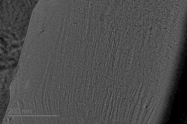
181 Figure A.11 TEM images of a sample with 5% PC in the electrolyte after 1 cycle. 161


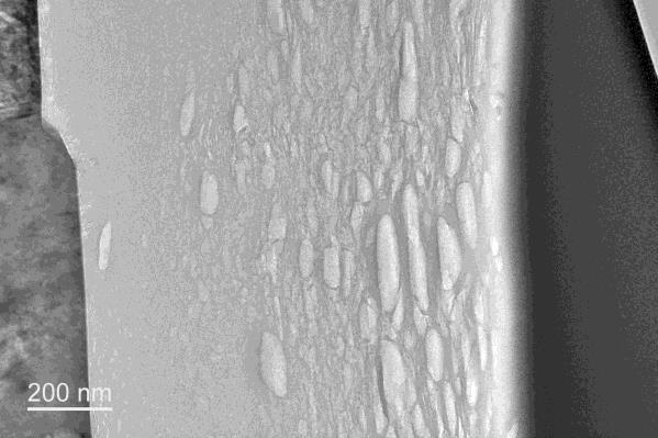
182 Figure A.12 TEM images of a sample with 10% PC in the electrolyte after 1 cycle. 162


183 Figure A.13 TEM images of a sample with 5% PC in the electrolyte after multipe cycles. 163
 As fabricated sample, (b) after a single cycle, (c) after Raman (laser burns the surface away during scan, structure is unstable).")


184 Figure A.14 Optical images of a sample that had PC added to electrolyte: (a) As fabricated sample, (b) after a single cycle, (c) after Raman (laser burns the surface away during scan, structure is unstable). Figure A.15 Raman data for a CVD sample, before cycling and after a single cycle with PC containg electolyte. (a) Raman data for the sample. (b) x-axis zoom on the two carbon peaks. These results are consistent with the previously observed results that show significant evidence of solvent co-intercalation, and are able to expand on previously published work through detailed observation of the resulting structure. First, while there is a report that showed PC does not disrupt the carbon structure if it is less than 20% of the electrolyte content 10, we are able to show that while the electrode is able to function at these concentrations, the structure is disrupted (and likely leads to large amount of SEI formation). The observations in the TEM images are particularly shocking since they show significant swelling in the electrode. When one considers the starting electrode thickness of around 300 nm, the resulting film with just 5% PC is able to expand to around 1 µm. Increasing PC content to 10% increases swelling. When the material is 164
185 observed up close one is able to see that the sheets of carbon are split and have pockets or amorphous material in between them, possibly SEI. Optical microscopy leads to the same conclusions with the surface looking much more uneven after cycling and Raman spectroscopy is able to further disrupt the surface (this is interesting since the laser is not able to damage the surface of the standard CVD film). Additionally, the Raman signature shown in Figure A.15 is consistent with TEM observations of local order while peak value decreases in overall magnitude after cycling. Figure A.16 Cycling data for PC containing electrolytes (a) control sample that contains no PC but has very similar cycling (previously shown in Figure 3.10) (b) 5% PC sample with a single cycle for TEM, (c) 10% PC sample with a single cycle for TEM, (d) 5% PC sample with longer cycling. The cycling and stress data contributes two useful observations. The first is the anomalous stress response at the start of the 0.5 V hold, which shows a tensile response. 165
186 This is below the potential of co-intercalation (and is likely the cause). The stranger part is when one reverses the potential the stress does not change, but when one reduces the potential the stress reverses and the behavior that follows is similar to that of the standard electrode. There is still significant capacity loss in the first cycle. The second observation is that the cycling in later cycles follows the same trends that are seen in standard carbon electrodes. With gradual SEI formation as seen in the standard electrolyte 14, the effect is small and stress during cycling is lower as is consistent with loss of active material. The conclusion for these experiments is that PC effects only the first cycle, and that once a stable structure is created the electrode behaves like a standard carbon electrode. It would be interesting to experiment with surface coating on CVD carbon. This would form an inorganic layer on the surface, which might be able to protect the surface of the electrode. A.4 Carbon Films with Modified PITT Analysis In this study coin cells were assembled at GM using 1M LiPF 6 EC:DMC electrolyte and pre-cycled, with 3 different schedules: fresh cell, pulse first cycle (see chapters 4 and 5 for explanation), and C/20 cycling. The resulting cells were then cycled using an identical schedule, with a series of voltage holds around 0.4V and 0.15V. There were a total of 5 holds around each potential at 5 mv increments: an example of the schedule is shown in Figure A.17. The voltage holds were then analyzed using a modified PITT technique 15 that was previously discussed in chapter 5. The resulting short term data was difficult to interpret since the capacity change was very small. To be 166
187 fit accurately and produce meaningful data, the useful time range was limited to ~0.2 seconds. An attempted fit of the data is shown in Figure A.18(a), and the summary of the resulting fit results plotted in Figure A.18(b). A long term fit was more successful and provided a reasonable trend in the data, although there were some difficulties with determining a usable data range (specifically differentiating between current going to carbon and background processes such as SEI formation). The results of the fits are shown in Figure A.19. The results have some scatter in the data, but the general trend is that fresh samples have a slower interface with more scatter in diffusion data. Pre-cycled samples were much more stable and showed the most consistent response. The pulse samples showed a fast interface, but also significant scatter in the results. Figure A.17 Example of the typical cycling schedule used to obtain the PITT data. 167
 Capactiy of the holds. (b) Fit results. A.")


188 Figure A.18 (a) Example of a short term fit. (b) Results of the short term fit. Figure A.19 Long term fit data. (a) Capactiy of the holds. (b) Fit results. A.5 Self-Discharge Experiments One of the follow-up projects to carbon work has been to look at carbon selfdischarge. This is the process during which the carbon films are able to spontaneously delithiate without the aid of current, at Open Circuit Potential / Voltage (OCP / OCV). This process has been modeled before and is partially reversible, but part of the lost Li goes to SEI formation 16. This is another method to probe SEI formation and an initial investigation has been carried out. For the initial experiment a series of OCV steps were 168
189 done after full lithiation (until 1 mv). In this case a regular galvanostatic cycle was interspaced between cycles with OCV steps in the cycling schedule. The resulting cycling data is plotted in Figure A.20 (a), with available stress data plotted in Figures A.20 (b and c). The initial results show that the sample is able to fully delithiate very slowly, as can be seen in the hold at around 600 hours. This is still faster than what has been previously suggested, and is consistent with thin film configuration vs. traditional particulate electrodes. The stress data is able to further explain the observed phenomenon. The continued stress response during the initial OCV steps suggests that SEI formation still continues even when the electrode is not cycling. Additionally, in later cycles the stress response is much more reversible suggesting that in later cycles Li loss and SEI formation are limited. 169
 cycling data for the entire experiment, (b) stress data for the initial OCV")

190 Figure A.20 Data for the first self-discharge experiment, (a) cycling data for the entire experiment, (b) stress data for the initial OCV holds, (c) stress data for later cycling data. A secondary follow-up experiment has been done that is related to the original experiment, but has much more varied cycling. The resulting cycling and stress data are shown in Figure A.21. First, multiple cycles were done initially to stabilize the SEI formation, followed by a long self-discharge step that allowed carbon to reach the second 170
191 plateau before cycling resumed. After further cycling and subsequent SEI stabilization more detailed experiments were done. First, a series of fast cycles were done during different stages of cycling interspaced with slower cycling. This allows some determination of interfacial kinetics over the course of cycling. Several plots of the faster cycling are shown in Figure A.22. Cyclic Voltammetry was also done after the sample was mostly stabilized and is shown in Figure A.23. The last set of experiments explored the open circuit behavior at different potentials. This was done by two methods. The first method involved cycling with potential holds, followed by a short OCV hold asshown in Figure A.24. The second method applied constant current for a short time period followed by an OCV hold asshown in Figure A.25. These results were able to contribute to the project, but a more detailed analysis would need to be developed to process this data. 171

192 Figure A.21 Cycling and stress data for the second sample described in A.5, parts (a-d) cycling data ordered sequentially. 172


193 Figure A.22 Examples of behavior during faster cycling at different states of the sample. Figure A.23 Cyclic Voltammetry on CVD carbon electrode after SEI stabilization (a) stress data, (b) current and stress data. 173
194 Figure A.24 OCV evolution after a voltage hold. (a) Comparison to galvanostatic cyling (b) Results of the cycling including stress data. (c) Repeat of the experiment at a later time. Figure A.25 OCV evolution after a periodic galvanostatic cycling. 174
195 A.6 References (1) Mukhopadhyay, A.; Tokranov, A.; Sena, K.; Xiao, X.; Sheldon, B. W. Thin Film Graphite Electrodes with Low Stress Generation during Li-Intercalation. Carbon N. Y. 2011, 49, (2) Ferrari, A.; Robertson, J. Interpretation of Raman Spectra of Disordered and Amorphous Carbon. Phys. Rev. B 2000, 61, (3) Tuinstra, F.; Koenig, J. L. Raman Spectrum of Graphite. J. Chem. Phys. 1970, 53, (4) Dillon, R. O.; Woollam, J. a. Use of Raman Scattering to Investigate Disorder and Crystallite Formation in as-deposited and Annealed Carbon Films. Phys. Rev. B 1984, 29, (5) Nemanich, R. J.; Glass, J. T.; Lucovsky, G.; Shroder, R. E. Raman Scattering Characterization of Carbon Bonding in Diamond and Diamondlike Thin Films. J. Vac. Sci. Technol. 1988, 6, (6) Guo, F.; Mukhopadhyay, A.; Sheldon, B. W.; Hurt, R. H. Vertically Aligned Graphene Layer Arrays from Chromonic Liquid Crystal Precursors. Adv. Mater. 2011, 23, (7) Guo, F.; Hurt, R. Supramolecular Synthesis of Graphenic Mesogenic Materials. Macromol. Chem. Phys. 2012, 213, (8) Mukhopadhyay, A.; Guo, F.; Tokranov, A.; Xiao, X.; Hurt, R. H.; Sheldon, B. W. Engineering of Graphene Layer Orientation to Attain High Rate Capability and Anisotropic Properties in Li-Ion Battery Electrodes. Adv. Funct. Mater. 2013, 23, (9) Dey, A. N.; Sullivan, B. P. The Electrochemical Decomposition of Propylene Carbonate on Graphite. J. Electrochem. Soc. 1970, 117, 222. (10) Von Wald Cresce, A.; Borodin, O.; Xu, K. Correlating Li+ Solvation Sheath Structure with Interphasial Chemistry on Graphite. J. Phys. Chem. C 2012, 116, (11) Wang, J.; Manga, K. K.; Bao, Q.; Loh, K. P. High-Yield Synthesis of Few-Layer Graphene Flakes through Electrolyte. J. Am. Chem. Soc. 2011, 133, (12) Flandrois, S.; Simon, B. Carbon Materials for Lithium-Ion Rechargeable Batteries. Carbon N. Y. 1999, 37,
196 (13) Nie, M.; Abraham, D. P.; Seo, D. M.; Chen, Y.; Bose, A.; Lucht, B. L. Role of Solution Structure in Solid Electrolyte Interphase Formation on Graphite with LiPF 6 in Propylene Carbonate. J. Phys. Chem. C 2013, 117, (14) Mukhopadhyay, A.; Tokranov, A.; Xiao, X.; Sheldon, B. W. Stress Development due to Surface Processes in Graphite Electrodes for Li-Ion Batteries: A First Report. Electrochim. Acta 2012, 66, (15) Li, J.; Xiao, X.; Yang, F.; Verbrugge, M. W.; Cheng, Y.-T. Potentiostatic Intermittent Titration Technique for Electrodes Governed by Diffusion and Interfacial Reaction. J. Phys. Chem. C 2012, 116, (16) Ramasamy, R. P.; Lee, J. W.; Popov, B. N. Simulation of Capacity Loss in Carbon Electrode for Lithium-Ion Cells during Storage. J. Power Sources 2007, 166,
197 APPENDIX B ADDITIONAL SILICON EXPERIMENTS B.1 Si Electrodes with FEC Electrolyte Additive One of the methods to improve surface passivation and alter the SEI layer is to add additives to electrolyte. While there are several options that are shown to have improved properties 1, the most common additive is fluoroethylene carbonate (FEC) 2,3. While there is a lot of evidence that this helps the battery, there are disagreements on the cause of this improvement 4 and how much additive is the right quantity 5,6. The results reported are often conflicting, with varying thicknesses reported 3,7 and different compositions There are a few factors the articles agree on: first, the electrolyte has a higher content of organic / polymeric components 3,4, and second, the SEI resistance measured by impedance after the SEI is stabilized is lower 6,9,11. These conflicting results are a source of much speculation and further experiments on the material are needed. Some work was done with FEC as part of this dissertation. The first experiment looked at the impact of FEC on SEI formation under the AFM (Figure B.1) as well some other comparable electrolytes. First, no SEI formation was observed at 0.9V. While SEI might decompose earlier, it was not observed. A thicker SEI layer is observed in the presence of FEC at 0.6V. This early SEI formation seems to have a significant impact on Li diffusion; more than the EC based material (see chapters 4 and 5). This can be better understood by referring to earlier work, where the optimal FEC additive quantity for thin 177

198 films was reported to be 1.5% 5. The idea behind FEC is that it is a reductive-type additive. It is meant to be consumed in the first cycle to create a more stable SEI layer. The optimal amount of FEC seems to be linked to the surface area, since the optimal amount seems to increase with a composite electrode 6. The same publication also reports that excessive amount of FEC seems to drop the capacity in the first couple of cycles. Figure B.1 Experimentally observed SEI growth during the first cycle at 0.6 V. The differences between electrolytes are observed with FEC creating the thickest SEI and roughest surface. The second series of experiments focused on PITT measurements discussed in Chapter 5. In this case there were two sets of experiments conducted: one with coin cells and one with MOSS cells. The results from the coin cells are shown in Figure B.2. These results are plotted vs. comparable results with standard electrolyte. Cycling is identical to that described in chapter 5. Follow up experiments with MOSS cells were done after the 178
199 initial results and added the stress measurement capability. For one specific experiment, a moderate length (2 hours) 0.6 V hold cycle was used during the first cycle. The resulting data along with a control electrolyte is plotted in Figure B.3 (in this case several hold lengths of control electrolyte are presented). In both of the above methods it is evident that the addition of FEC results in a slightly slower interface. This agrees very well with previous findings from this work and supports the model proposed in chapter 5: the thick SEI is derived from reduction FEC, which is self-passivating, but the resulting material will drop rate capability until inorganic SEI is able to grow through the organic material. Figure B.2 Summary of PITT results for coin cells during the 4 th cycle. 179
200 Figure B.3 Summary of PITT results for MOSS cells (this is the average of 3 cycles after the 1 st cycle). The MOSS cells were also able to record the curvature of the film and provide a stress response. While the SEI stress response is not seen due to the large Si stress response, the rate of lithiation can be seen. Stress response is plotted in Figure B.4(a) for a film with FEC and a control without. Both films show similar trends, but the FEC sample has a delayed initial response at higher cell voltages. This is seen again in Figure B.4(b), where a longer hold at high potential is used. The stress response seen is likely amorphous Si phase transformation 12,13, and is likely slower in the FEC electrolyte due to the initial thicker SEI formed. In extreme case (when a very thick SEI is formed using FEC), a much slower stress can be observed, Figure B.4(c). This anomalous behavior needs further investigation. Figure B.5 summarizes the final stress state of the samples at constant potential and shows that results are repeatable across samples. 180
201 Figure B.4 (a-b) Stress data of the first cycle, impact of electrolyte on rate of phase transformation. (c) Later cycles comparison. A significant delay in stress response can be seen. Figure B.5 (a) Measured stress thickness and (b) Estimated stress in Si electrodes (this is the average of 3 cycles after the 1 st cycle). 181
202 The impact of FEC was also analyzed by EIS measurements using the same cycling and technique as described in section 5. The resulting electrolyte contained 10% FEC added to it. The results can be broken down into two sections: the initial SEI formation and evolution in later cycles. The data taken during the first cycle is shown for both the control and 10% FEC, slow cycling in Figure B.6(a), and pulse in Figure B.6(b). These results show that FEC has higher resistance than electrolyte without FEC addition for both of the cycling schedules. The second data set focuses on later cycling This can be represented in two ways: first as a change of resistance with each cycle (Figure B.7), and second as 1/R, the conductivity, which represents Li flux for the electrodes (Figure B.8). The results presented show that FEC addition produces higher SEI resistance, contrary to previously reported data. Figure B.6 Resistance increase during a voltage hold in the first cycle: (a) 0.6V, (b) 0.05V. 182
203 Figure B.7 Resistance in the later cycles (with 10 % FEC) with fast cycling (a), sample with slow first cycle (b), comparison of the two (c), comparison of samples with identical cycle but no FEC (d). Figure B.8 SEI conductivity changes with cycle number (with and without FEC). (a) slow cycling, (b) Pulse cycling. 183

204 Further analysis by AFM results are shown below. This includes AFM PITT analysis described in detail in chapter 5. The results are shown in Figure B.9, and show that FEC is also causing slower lithiation in this system, which is especially evident in slow SEI cycling. Additionally, mechanical properties of near surface SEI have been measured and are similar to what is reported in chapter 5, with identical trends (Figure B.10). The fast cycling does not exhibit any significant change to SEI properties while slower cycling is shown to have a significant increase in deformation and a large decrease in the DMTModulus. Figure B.9 PITT fit results for the AFM lithiation. 184
205 Figure B.10 AFM mechanical properties (a) deformation for slow cycling, (b) DTModulus for slow cycling, and (c) deformation for pulse cycling. There has been a significant amount of data reported on FEC as an additive and solvent in electrolyte. Almost all agree on improved performance, with possible exception of battery safety 14. Most of the publications that do analysis on SEI report a polymeric material, mostly polycarbonates 5,15, which is almost always accompanied by LiF 7,8,16. Regular SEI without FEC additive has lower oxygen content and is thinner. There is also TEM data showing insoluble polymeric species as a nanocomposite in the SEI 8. Later cycles also have lower SEI resistance when measured by EIS, which is consistent with LiF having higher electrical conductivity. However, there is no agreement on which properties are the cause of improvement. 185
206 The question that remains to be answered is what characteristic of SEI is causing the benefit. There are a few possibilities. The first is that the polymeric material is able to bridge cracks in the SEI, preventing liquid from accessing the surface, as reported for addition of vinylene carbonate (VC) 17,18. While our results show that the FEC-based SEI does slow electrolyte diffusion, the electrolyte still has access to the surface. The second possibility is that the FEC SEI is acting as a buffer. It is possible that the polymeric SEI is causing slower diffusion and as a result prevents overpotential in the electrode. This decreases stress concentrations and overcharging, which is considered an issue due to particle size distributions. The last possibility is mechanical stability could be improved this could be due to polymeric material acting as an elastomer, or different salt content in the SEI. This work indicates that a combination of these factors result in the overall benefit. The last parameter to address is the cycling in the first cycle. By increasing the cycling rate, the organic SEI formation is decreased and a more inorganic SEI that seems to have superior diffusion properties is formed. This allows one to optimize the SEI with suboptimal amount of additives through cycling. This process can also be further refined to cause a certain amount of organic to form after which the current would be increase, cutting off further formation. 186
207 B.2 Anamalous Silicon Stress Response During Voltage Holds It has been observed while running MOSS cells with Si thin films that the stress has an unusual response when cell voltage is in the region of silicon flow. Initial results presented in Figure B.11 show that stress and current in the MOSS cell are linked. Figure B.11 Initial observations of stress and current trends during a voltage hold. These initial results triggered some follow up experiements to look at this phenomenon over the course of several cycles. For thisexperiment a 50 nm film was used with 1M LiPF 6 in EC:DMC electrolyte and the cycling was repeating a series of potential holds over multiple cycles. The results of the first experiment are shown in Figure B.12. For this experiment every odd number cycle was a series of potential holds for which stress and current were analysed. The even numbered holds were pulse cycles meant to quickly cycle the electrode. An additional expereiment was run to repeat the observations made in the first expereiment (Figure B.13). The resulting current data was analysed using the PITT technique previously described in section 5 (Figure B.14). 187

208 Figure B.12 Change in current and stress response for a silicon sample over several cycles. (a and b) Current and stress data for 0.9 V 0.6 V hold. (c and d) Current and stress data for 0.1 V 0.05 V hold. While these results are not complete, there are a couple of observations that can be made. At higher potential ( 0.4 V) the stress seems to behave elastically and the current response is as expected. Once material starts to flow the stress and current response become more complicated. Specifically, while the initial ~10 seconds is consistent with an elastic response, it seem to peak shortly after. This is likely due to the initiation of a flow mechanism, and corresponds to a current low point. In the following minute, current is increasing while stress seems to relax, after which current peaks 188
209 followed by a steady decrease. During this time stress response depends on the potential, but seems to resemble silicon flow. Figure B.13 Change in current and stress response for a silicon sample over several cycles. (a and b) Current and stress data for 0.1 V 0.05 V hold. (c and d) Current and stress data for 0.2 V 0.1 V hold. 189
210 Figure B.14 Results from fitting the modified PITT model to the capacity data for the Si thin film electrodes (a) Li ion diffusivity (b) Biot Number (c) Capacity. The current and stress flow behavior described above has been seen in several samples and is reasonably consistent. When the samples are examined with modified PITT this stress response greatly impacts the Biot number. A large difference can be observed between holds above 0.4V hold and the ones below 0.4V. This behavior has an impact on transport properties, but further observations are needed before any conclusions are made. 190

211 B.3 Initial Si SEI Experiments Some initial SEI investigation with the use of MOSS stress measurements was attempted in the initial stages of research. This was done on 7 µm Si island samples 19, through cycling the sample at SEI forming potentials, but above Si lithiation potential. The subsequent cycling slowly lowered the cycling potential, increasing Si lithiation. The idea behind this experiment was to see whether the point at which SEI breaks can be observed. This is due to larger expansion of Si at lower potentials, which would stress the SEI (Figure B.15). The results from the experiment shown in Figure B.16 show that a large stress response is visible, although and the results are hard to explain. Specifically, it is unclear why there is an extremely large stress increase after the electrode is cycled to lower potential. After cycling the sample was examined under SEM and AFM (Figure B.17) and was observed to show some fiber formation. Figure B.15 Schematic showing the initially proposed SEI degradation on silicon. 191
212 Figure B.16 Potential and stress response of the initial SEI experiments. 192


213 Figure B.17 Post mortem analysis of the islands sample using SEM and TEM. The results were intriguing and a second experiment was attempted. In this case cycling was longer and most of the initial experiments were at a higher potential to see if the SEI provided a stress response. The results are shown in Figure B.18. Since the resulting data set is difficult to view in a single plot, several smaller plots were used. The results show almost no stress response during cycling until lower potential, where the large stress response was again observed, followed by significant capacity loss. To study this post mortem SEM, and TEM cross-sections were done and are shown in Figure B.19 and Figure B.20. A SEI layer that is much thicker than the original electrode height can 193
214 be seen. The resulting thickness can only be explained by extensive SEI formation. The cycling data shows a large decrease in capacity after full lithiation. This implies that the SEI is able to constrict the Si electrode and causes critical failure at lower potential. To address these observations a revised model is proposed in Figure B.21. Due to time constraints the project was not further pursued. 194


215 Figure B.18 Potential and stress response of the second SEI experiments. 195

 top-down view, (b)")
216 Figure B.19 SEM view of the islands after cycling (a) top-down view, (b) FIB crosssection. 196

 single")

217 (a) (b) Figure B.20 TEM view of the islands after cycling (a) single image, (b) composite encompassing the entire island. 197
 Lin, Y.-M.; Klavetter, K. C.; Abel, P. R.; Davy, N.")
218 Figure B.21 Schematic showing the revised SEI degradation mechanism on silicon. B.4 References (1) Dalavi, S.; Guduru, P.; Lucht, B. L. Performance Enhancing Electrolyte Additives for Lithium Ion Batteries with Silicon Anodes. J. Electrochem. Soc. 2012, 159, A642 A646. (2) Lin, Y.-M.; Klavetter, K. C.; Abel, P. R.; Davy, N. C.; Snider, J. L.; Heller, A.; Mullins, C. B. High Performance Silicon Nanoparticle Anode in Fluoroethylene Carbonate-Based Electrolyte for Li-Ion Batteries. Chem. Commun. 2012, 48, (3) Etacheri, V.; Haik, O.; Goffer, Y.; Roberts, G. A.; Stefan, I. C.; Fasching, R.; Aurbach, D. Effect of Fluoroethylene Carbonate (FEC) on the Performance and Surface Chemistry of Si-Nanowire Li-Ion Battery Anodes. Langmuir 2012, 28,
In-situ Study of Solid Electrolyte Interphase on Silicon Electrodes using PeakForce Tapping Mode AFM in Glove-box
 General Motors R&D BROWN UNIVERSITY In-situ Study of Solid Electrolyte Interphase on Silicon Electrodes using PeakForce Tapping Mode AFM in Glove-box A. Tokranov 1, X. Xiao 2, C. Li 3, S. Minne 3 and B.
High Performance Lithium Battery Anodes Using Silicon Nanowires
 Supporting Online Materials For High Performance Lithium Battery Anodes Using Silicon Nanowires Candace K. Chan, Hailin Peng, Gao Liu, Kevin McIlwrath, Xiao Feng Zhang, Robert A. Huggins and Yi Cui * *To
Investigation of anode materials for lithium-ion batteries
 University of Wollongong Thesis Collections University of Wollongong Thesis Collection University of Wollongong Year 2006 Investigation of anode materials for lithium-ion batteries Ling Yuan University
Carbon-Silicon Core-Shell Nanowires as High Capacity Electrode for Lithium Ion Batteries
 Carbon-Silicon Core-Shell Nanowires as High Capacity Electrode for Lithium Ion Batteries NANO LETTERS XXXX Vol. xx, No. x - Li-Feng Cui, Yuan Yang, Ching-Mei Hsu, and Yi Cui* Department of Materials Science
Elucidating the Phase Transformation of Li4Ti5O12 Lithiation at the Nanoscale
 Elucidating the Phase Transformation of Li4Ti5O12 Lithiation at the Nanoscale Michael G. Verde 1*, Loïc Baggetto 2, Nina Balke 3, Gabriel M. Veith 2, Joon Kyo Seo 4, Ziying Wang 1, Ying Shirley Meng 1*
Supplementary Figure 1:
 b a c Supplementary Figure 1: Calibration of the Cs + sputtering rate on composite LiNi 0.7 Mn 0.15 Co 0.15 O 2 electrodes (500 ev ion energy, ~40 na measured sample current): (a) Optical profilometry
Nanocomposites as next-generation anode materials for lithium ion batteries
 Nanocomposites as next-generation anode materials for lithium ion batteries Lorenzo Mangolini Mechanical Engineering Department Materials Science and Engineering Program UC Riverside International Battery
Microscopic Structural Analysis of Advanced Anode Material for Lithium Battery
 JFE TECHNICAL REPORT No. 22 (Mar. 2017) Microscopic Structural Analysis of Advanced Anode Material for Lithium Battery SIMAUCHI Yutaka *1 OHMORI Shigekazu *2 IKEMOTO Sachi *3 Abstract: analyzed the microstructure
6th International Conference on Advanced Design and Manufacturing Engineering (ICADME 2016)
") 6th International Conference on Advanced Design and Manufacturing Engineering (ICADME 2016) Porous Co3O4 irregular Micro-cubes with lithium storage performances Ting Wanga, Hao Zhengb, Jinsong Chengc,
6th International Conference on Advanced Design and Manufacturing Engineering (ICADME 2016) Porous Co3O4 irregular Micro-cubes with lithium storage performances Ting Wanga, Hao Zhengb, Jinsong Chengc,
ALD TiO 2 coated Silicon Nanowires for Lithium Ion Battery Anodes with enhanced Cycling Stability and Coulombic Efficiency
 ALD TiO 2 coated Silicon Nanowires for Lithium Ion Battery Anodes with enhanced Cycling Stability and Coulombic Efficiency Elmira Memarzadeh Lotfabad a, Peter Kalisvaart a,*, Kai Cui b, Alireza Kohandehghan
On the Role of Mechanics in the Design and Performance of Electrode Materials for Energy Storage
 On the Role of Mechanics in the Design and Performance of Electrode Materials for Energy Storage Pradeep R. Guduru School of Engineering, Brown University V. Sethuraman, M. Chon, S. Nadimpalli Collaborators:
PHYSICAL REVIEW LETTERS 107,
 Real-time Measurement of Stress and Damage Evolution During Initial Lithiation of Crystalline Silicon M. J. Chon, 1 V.A. Sethuraman, 1 A. McCormick, 1 V. Srinivasan, 2 P. R. Guduru 1,* 1 School of Engineering,
De-ionized water. Nickel target. Supplementary Figure S1. A schematic illustration of the experimental setup.
 Graphite Electrode Graphite Electrode De-ionized water Nickel target Supplementary Figure S1. A schematic illustration of the experimental setup. Intensity ( a.u.) Ni(OH) 2 deposited on the graphite blank
In Situ Formation of Stable Interfacial Coating for High Performance Lithium Metal Anodes
 In Situ Formation of Stable Interfacial Coating for High Performance Lithium Metal Anodes Haiping Wu 1, Yue Cao 1, Linxiao Geng 2 & Chao Wang 1* 1 Department of Chemistry, University of California Riverside,
SUPPORTING INFORMATION. A Rechargeable Aluminum-Ion Battery Based on MoS 2. Microsphere Cathode
 SUPPORTING INFORMATION A Rechargeable Aluminum-Ion Battery Based on MoS 2 Microsphere Cathode Zhanyu Li a, Bangbang Niu a, Jian Liu a, Jianling Li a* Feiyu Kang b a School of Metallurgical and Ecological
Supporting Information
 Supporting Information Garnet electrolyte with an ultra-low interfacial resistance for Li-metal batteries Yutao Li, Xi Chen, Andrei Dolocan, Zhiming Cui, Sen Xin, Leigang Xue, Henghui Xu, Kyusung Park,
Improving cyclic performance of Si anode for lithium-ion batteries by forming an intermetallic skin
 Electronic Supplementary Material (ESI) for RSC Advances. This journal is The Royal Society of Chemistry 2015 Supporting Information Improving cyclic performance of Si anode for lithium-ion batteries by
Silver Diffusion Bonding and Layer Transfer of Lithium Niobate to Silicon
 Chapter 5 Silver Diffusion Bonding and Layer Transfer of Lithium Niobate to Silicon 5.1 Introduction In this chapter, we discuss a method of metallic bonding between two deposited silver layers. A diffusion
Supporting Information
 Supporting Information Hydrogenation Driven Conductive Na 2 Nanoarrays as Robust Binder-Free Anodes for Sodium-Ion Batteries Shidong Fu, Jiangfeng Ni, Yong Xu, Qiao Zhang*, and Liang Li*, College of Physics,
Supplementary Figure 1 The lithium polysulfide distribution on the patterned electrode.
 Supplementary Figure 1.The lithium polysulfide distribution on the patterned electrode. SEM image of the ITO-carbon electrode after dipping into Li 2 S 8 solution and drying, which shows the random distribution
Dramatically enhanced reversibility of Li 2 O in SnO 2 -based electrodes: the effect of nanostructure on high initial reversible capacity
 Electronic Supplementary Material (ESI) for Energy & Environmental Science. This journal is The Royal Society of Chemistry 2015 Electronic supplementary information for Dramatically enhanced reversibility
Electroactive Polymer for Controlling Overcharge in Lithium-Ion Batteries
 PSI-SR-1261 Electroactive Polymer for Controlling Overcharge in Lithium-Ion Batteries A. Newman R. Pawle K. White J. Lennhoff A. Newman, R. Pawle, K. White, J. Lennhoff, "Electroactive Polymer for Controlling
Electronic supplementary information. Efficient energy storage capabilities promoted by hierarchically MnCo 2 O 4
 Electronic Supplementary Material (ESI) for RSC Advances. This journal is The Royal Society of Chemistry 2014 Electronic supplementary information Efficient energy storage capabilities promoted by hierarchically
Rice husks as a sustainable source of nanostructured silicon for high performance Li-ion battery anodes
 Supplementary Information Rice husks as a sustainable source of nanostructured silicon for high performance Li-ion battery anodes Nian Liu 1, Kaifu Huo 2,3, Matthew T. McDowell 2, Jie Zhao 2 & Yi Cui 2,4
High Rate and Durable, Binder Free Anode Based on Silicon Loaded MoO 3 Nanoplatelets
 Supplementary Information High Rate and Durable, Binder Free Anode Based on Silicon Loaded O 3 Nanoplatelets Alejandro Martinez-Garcia, Arjun Kumar Thapa,Ruvini Dharmadasa,, Tu Q. Nguyen, Jacek Jasinski,
SUPPLEMENTARY INFORMATION
 High Electrochemical Activity of the Oxide Phase in Model Ceria- and Ceria-Ni Composite Anodes William C. Chueh 1,, Yong Hao, WooChul Jung, Sossina M. Haile Materials Science, California Institute of Technology,
From Surface To Cell: Understanding the Lithium Ion Battery. The world leader in serving science
 From Surface To Cell: Understanding the Lithium Ion Battery 1 The world leader in serving science Content Discharge Detail the Li-ion Battery industry drivers & trends Our position in industry and our
Supporting information
 Electronic Supplementary Material (ESI) for Energy & Environmental Science. This journal is The Royal Society of Chemistry 2015 Supporting information A Low Temperature Molten Salt Process for Aluminothermic
State of Lithium Ion Battery Research
 State of Lithium Ion Battery Research Professor Vanessa Wood Department of Information Technology and Electrical Engineering ETH Zürich 2/5/2018 1 Lithium ion batteries can be used for many applications
Ceramic Processing Research
 Journal of Ceramic Processing Research. Vol. 17, No. 11, pp. 1192~1196 (2016) J O U R N A L O F Ceramic Processing Research Degradation mechanism of the complementary electrochromic devices with WO 3 and
Urchin-like V 2 O 3 /C Hollow Nanospheres Hybrid for High-Capacity and Long-Cycle-Life Lithium Storage
 Supporting Information Urchin-like V 2 O 3 /C Hollow Nanospheres Hybrid for High-Capacity and Long-Cycle-Life Lithium Storage Peng Yu, Xu Liu, Lei Wang,* Chungui Tian, Haitao Yu, and Honggang Fu* Key Laboratory
Sn Wears Super Skin: A New Design For Long Cycling Batteries
 Supporting Information Wears Super Skin: A New Design For Long Cycling Batteries Shuai Kang, Xi Chen, Junjie Niu* Department of Materials Science and Engineering, CEAS, University of Wisconsin-Milwaukee
Factors Influencing the Thermal Stability of Lithium Ion Batteries - From Active Materials to State-of-Charge and Degradation
 Factors Influencing the Thermal Stability of Lithium Ion Batteries - From Active Materials to State-of-Charge and Degradation JRC Exploratory Research Workshop Safer Li-Ion Batteries by Preventing Thermal
Supporting Information
 Supporting Information In Situ-formed Li 2 S in Lithiated Graphite Electrodes for Lithium-Sulfur Batteries Yongzhu Fu, Chenxi Zu, Arumugam Manthiram Electrochemical Energy Laboratory & Materials Science
components and inorganic Li salts from PST-90. When contacting with Li metal, PST-
 Supplementary Figure 1. Proposed mechanism for the formation of organic components and inorganic Li salts from PST-90. When contacting with Li metal, PST- 1 90 first generates high order organopolysulfide
Supporting Information
 Electronic Supplementary Material (ESI) for Energy & Environmental Science. This journal is The Royal Society of Chemistry 2018 Supporting Information High performance All-Solid-State Li-Se Batteries induced
All-solid-state Li battery using a light-weight solid electrolyte
 All-solid-state Li battery using a light-weight solid electrolyte Hitoshi Takamura Department of Materials Science, Graduate School of Engineering, Tohoku University Europe-Japan Symposium, Electrical
Factors Governing Life of High-Energy Lithium-Ion Cells
 Factors Governing Life of High-Energy Lithium-Ion Cells D.P. Abraham IBA 2013 March 11, 2013 Barcelona, Spain Research sponsors are both Government and Private Sector 2 Diagnostics Overview Use of characterization
Effect of heat treatment on electrochemical characteristics of spinel lithium titanium oxide
 Korean J. Chem. Eng., 27(1), 91-95 (2010) DOI: 10.1007/s11814-009-0298-0 RAPID COMMUNICATION Effect of heat treatment on electrochemical characteristics of spinel lithium titanium oxide Sung-Chul Hong*,
Electronic Supplementary Information (ESI) Self-assembly of Polyoxometalate / Reduced Graphene Oxide
 Self-assembly of Polyoxometalate / Reduced Graphene Oxide") Electronic Supplementary Material (ESI) for Journal of Materials Chemistry A. This journal is The Royal Society of Chemistry 2017 Electronic Supplementary Information (ESI) Self-assembly of Polyoxometalate
Electronic Supplementary Material (ESI) for Journal of Materials Chemistry A. This journal is The Royal Society of Chemistry 2017 Electronic Supplementary Information (ESI) Self-assembly of Polyoxometalate
Supporting Information. Amorphous Red Phosphorus Embedded in Highly Ordered. Mesoporous Carbon with Superior Lithium and Sodium Storage.
 Supporting Information Amorphous Red Phosphorus Embedded in Highly Ordered Mesoporous Carbon with Superior Lithium and Sodium Storage Capacity Weihan Li, Zhenzhong Yang, Minsi Li, Yu Jiang, Xiang Wei,
School of Materials Science and Engineering, South China University of Technology,
 Supporting information Zn/MnO 2 Battery Chemistry With H + and Zn 2+ Co-Insertion Wei Sun, Fei Wang, Singyuk Hou, Chongyin Yang, Xiulin Fan, Zhaohui Ma, Tao Gao, Fudong Han, Renzong Hu, Min Zhu *, Chunsheng
Overview of research
 MICDE-TARDEC Faculty Workshop Overview of research Wei Lu Mechanical Engineering University of Michigan, Ann Arbor weilu@umich.edu September 15, 2017 1 Overall of Research Areas Joining of dissimilar materials,
Corrosion. Lab. of Energy Conversion & Storage Materials. Produced by K. B. Kim
 Corrosion 대기환경에의한금속소재 (organic film coated steel) 의퇴화현상평가연구 Lab. of Energy Conversion & Storage Materials Produced by K. B. Kim Introduction AC Impedance Spectroscopy Application of AC Impedance to Corrosion
Soft silicon anodes for lithium ion batteries
 Electronic Supplementary Material (ESI) for Energy & Environmental Science. This journal is The Royal Society of Chemistry 2014 Supplementary Information Soft silicon anodes for lithium ion batteries Qizhen
The Quantitative Evaluation of Anode Thickness Change for Lithium-ion Batteries
 The Quantitative Evaluation of node Thickness Change for Lithium-ion atteries Hiroko Takahashi* 1, Masanobu ragaki* 1, Toshiya Hikami* 2 The measurement technique of the electrode thickness to measure
Doped Si nanoparticles with conformal. and high-rate lithium-ion battery anodes
 Nanotechnology Nanotechnology 26 (2015) 365401 (6pp) doi:10.1088/0957-4484/26/36/365401 Doped Si nanoparticles with conformal carbon coating and cyclizedpolyacrylonitrile network as high-capacity and high-rate
Supporting Information
 Supporting Information Spherical Li Deposited inside 3D Cu Skeleton as Anode with Ultra-Stable Performance Yanyan Wang, 1 Zhijie Wang, 1 Danni Lei, 1,2 Wei Lv, 1 Qiang Zhao, 1,2 Bin Ni, 1,2 Yong Liu, 3
Supplementary Information. Capacity fade in high energy silicon-graphite electrodes for lithium-ion batteries
 Electronic Supplementary Material (ESI) for ChemComm. This journal is The Royal Society of Chemistry 2018 Supplementary Information Capacity fade in high energy silicon-graphite electrodes for lithium-ion
SUPPLEMENTARY INFORMATIONS
 SUPPLEMENTARY INFORMATIONS Dynamic Evolution of Conducting Nanofilament in Resistive Switching Memories Jui-Yuan Chen, Cheng-Lun Hsin,,, Chun-Wei Huang, Chung-Hua Chiu, Yu-Ting Huang, Su-Jien Lin, Wen-Wei
Supplementary Figure 1. Crystal structures of conventional layered and Li-rich layered manganese oxides. a, The crystal structure of rhombohedral
 Supplementary Figure 1. Crystal structures of conventional layered and Li-rich layered manganese oxides. a, The crystal structure of rhombohedral LiMO 2 (M = Ni, Co, Mn) with the space group R3m. b, The
Experiences of PLD Technology for LIB Separators. PICODEON Oy. Neal White
 Experiences of PLD Technology for LIB Separators PICODEON Oy Neal White 1 Outline Introduction to Picodeon Ceramic coating rationale Separator overview Why PLD for LIB separators Current status of Picodeon
FABRICATION AND ELECTROCHEMICAL CHARECTARIZATION OF THE CR2032 COIN CELLS USING THE DEVELOPED PURE AND CARBON COATED
 FABRICATION AND ELECTROCHEMICAL CHARECTARIZATION OF THE CR2032 COIN CELLS USING THE DEVELOPED PURE AND CARBON COATED LiMPO 4 (M= Mn, Co & Ni) NANOPARTICLES CHAPTER VI 181 CHAPTER - VI FABRICATION AND ELECTROCHEMICAL
Fundamental Study on Li Metal Dissolution and Deposition on Cu Foil in Nonaqueous Electrolytes with 3DOM Separator
 217 BLI X, Symposium on Energy Storage, June 27-29, 217, at IBM- Research Almaden in San Jose, CA, USA Fundamental Study on Li Metal Dissolution and Deposition on Cu Foil in Nonaqueous Electrolytes with
Amorphous and Nanocrystalline Mg 2 Si Thin Film Electrodes
 Manuscript# IMLB-070, LBNL-52142 Revised to Journal of Power Sources (Dec 13, 2002) Amorphous and Nanocrystalline Mg 2 Si Thin Film Electrodes Seung-Wan Song, a Kathryn A. Striebel, a,z Xiangyun Song a
In situ generation of Li 2 FeSiO 4 coating on MWNT as a high rate cathode material for lithium ion batteries
 Supporting Information: In situ generation of Li 2 FeSiO 4 coating on MWNT as a high rate cathode material for lithium ion batteries Yi Zhao, Jiaxin Li, Ning Wang, Chuxin Wu, Yunhai Ding, Lunhui Guan*
Supporting Information
 Supporting Information Designing hybrid NiP 2/NiO nanorod arrays for efficient alkaline hydrogen evolution Meng-Ying Wu, Peng-Fei Da, Tong Zhang, Jing Mao,*, Hui Liu,*, and Tao Ling,*, Key Laboratory for
IBM Almaden June 27, Seongmin Ha, Dongho Koo, Kyu Tae Lee * Chemical and Biological Engineering Seoul National University
 IBM Almaden June 27, 2017 Seongmin Ha, Dongho Koo, Kyu Tae Lee * Chemical and Biological Engineering Seoul National University (ktlee@snu.ac.kr) 1) Introduction 2) Failure mechanism of a redox mediator
Chapter 7. Evaluation of Electrode Performance by. Electrochemical Impedance
 Chapter 7 Evaluation of Electrode Performance by Electrochemical Impedance Spectroscopy (EIS) 7.1 Introduction A significant fraction of internal resistance of a cell comes from the interfacial polarization
Supporting Information
 Supporting Information Earth Abundant Fe/Mn-Based Layered Oxide Interconnected Nanowires for Advanced K-Ion Full Batteries Xuanpeng Wang, Xiaoming Xu, Chaojiang Niu*, Jiashen Meng, Meng Huang, Xiong Liu,
Final Report for FA Carbon-coated current collectors for high-power Li-ion secondary batteries /29
 Final Report for FA2386-11-1-4100 Carbon-coated current collectors for high-power Li-ion secondary batteries 2012.8/29 Name of Principal Investigators: - e-mail address : nlw001@ntu.edu.tw - Institution
Novel Mn 1.5 Co 1.5 O 4 spinel cathodes for intermediate temperature solid oxide fuel cells
 Novel Mn 1.5 Co 1.5 O 4 spinel cathodes for intermediate temperature solid oxide fuel cells Huanying Liu, a, b Xuefeng Zhu, a * Mojie Cheng, c You Cong, a Weishen Yang a * a State Key Laboratory of Catalysis,
Supporting Information
 Copyright WILEY VCH Verlag GmbH & Co. KGaA, 69469 Weinheim, Germany, 2012. Supporting Information for Small, DOI: 10.1002/smll. 201102654 Large-Area Vapor-Phase Growth and Characterization of MoS 2 Atomic
Supporting Information. for Efficient Low-Frequency Microwave Absorption
 Supporting Information Facile Hydrothermal Synthesis of Fe 3 O 4 /C Core-Shell Nanorings for Efficient Low-Frequency Microwave Absorption Tong Wu,, Yun Liu, Xiang Zeng, Tingting Cui, Yanting Zhao, Yana
The Li-O 2 Battery with a Dimethylformamide Electrolyte
 The Li-O 2 Battery with a Dimethylformamide Electrolyte Yuhui Chen, Stefan A. Freunberger, Zhangquan Peng, Fanny Bardé and Peter G. Bruce* School of Chemistry, University of St. Andrews, North Haugh, St.
Supporting information
 Electronic Supplementary Material (ESI) for Nanoscale. This journal is The Royal Society of Chemistry 2018 Supporting information An amorphous material with sponge-like structure as anode for Liion and
A Brief History of Non-aqueous Metal-Air Batteries
 67 ECS Transactions, 3 (42) 67-71 (2008) 10.1149/1.2838193, copyright The Electrochemical Society A Brief History of Non-aqueous Metal-Air Batteries K. M. Abraham E-KEM Sciences Needham, MA 02492, USA
image of ZMO precursor/rgo. Scale bar, 50 nm. (b) XRD patterns of reduced graphene
 XRD patterns of reduced graphene") Supplementary Figures Supplementary Figure 1 Characterization of ZMO precursor/rgo. (a) STEM image of ZMO precursor/rgo. Scale bar, 50 nm. (b) XRD patterns of reduced graphene oxide (rgo) and ZMO precursor/rgo.
Supplementary Figures Supplementary Figure 1 Characterization of ZMO precursor/rgo. (a) STEM image of ZMO precursor/rgo. Scale bar, 50 nm. (b) XRD patterns of reduced graphene oxide (rgo) and ZMO precursor/rgo.
Supporting Information for
 Supporting Information for Self-stabilized solid electrolyte interface on host-free Li metal anode towards high areal capacity and rate utilization Zhenglin Hu 1,3, Shu Zhang 1, Shanmu Dong*,1, Quan Li
Safe, Inexpensive, Long Life, High Power and Efficiency Batteries For Grid Scale Energy Storage Applications
 Safe, Inexpensive, Long Life, High Power and Efficiency Batteries For Grid Scale Energy Storage Applications Investigators Yi Cui, Associate Professor; Robert Huggins, Professor; Mauro Pasta, Postdoctoral
The Coating Effects of Al 2 O 3 on a Li[Li 0.2 Mn 0.54 Co 0.13 Ni 0.13 ]O 2 Surface Modified with (NH 4 ) 2 SO 4
![The Coating Effects of Al 2 O 3 on a Li[Li 0.2 Mn 0.54 Co 0.13 Ni 0.13 ]O 2 Surface Modified with (NH 4 ) 2 SO 4](/thumbs/93/111425442.jpg "The Coating Effects of Al 2 O 3 on a Li[Li 0.2 Mn 0.54 Co 0.13 Ni 0.13 ]O 2 Surface Modified with (NH 4 ) 2 SO 4") 1516 Bull. Korean Chem. Soc. 2014, Vol. 35, No. 5 Ji-Woo Oh et al. http://dx.doi.org/10.5012/bkcs.2014.35.5.1516 The Coating Effects of Al 2 O 3 on a Li[Li 0.2 Mn 0.54 Co 0.13 Ni 0.13 ]O 2 Surface Modified
1516 Bull. Korean Chem. Soc. 2014, Vol. 35, No. 5 Ji-Woo Oh et al. http://dx.doi.org/10.5012/bkcs.2014.35.5.1516 The Coating Effects of Al 2 O 3 on a Li[Li 0.2 Mn 0.54 Co 0.13 Ni 0.13 ]O 2 Surface Modified
Ruthenium Oxide Films Prepared by Reactive Biased Target Sputtering
 Ruthenium Oxide Films Prepared by Reactive Biased Target Sputtering Hengda Zhang Anthony Githinji 1. Background RuO2 in both crystalline and amorphous forms is of crucial importance for theoretical as
EFFECT OF THE PITCH-BASED CARBON ANODE ON THE IRREVERSIBLE CAPACITY OF LITHIUM-ION SECONDARY BATTERY
 EFFECT OF THE PITCH-BASED CARBON ANODE ON THE IRREVERSIBLE CAPACITY OF LITHIUM-ION SECONDARY BATTERY Weiming Lu and D.D.L. Chung Composite Materials Research Laboratory University at Buffalo The State
Topic: Electrochemical Application of Carbon Materials MILD-EXFOLIATED GRAPHITE AS AN ANODE MATERIAL FOR LITHIUM ION BATTERY.
 Paper ID: 373 Topic: Electrochemical Application of Carbon Materials MILD-EXFOLIATED GRAPHITE AS AN ANODE MATERIAL FOR LITHIUM ION BATTERY Lin Zou, Yong-Ping Zheng, Feiyu Kang, Wanci Shen, Can Xu Laboratory
A Robust Hybrid Zn-Battery with Ultralong Cycle Life
 A Robust Hybrid Zn-Battery with Ultralong Cycle Life Bing Li, a Junye Quan, b Adeline Loh, #a Jianwei Chai, a Ye Chen, b Chaoliang Tan, b Xiaoming Ge, a T. S. Andy Hor, a,c Zhaolin Liu, *a Hua Zhang *b
Three-dimensional graphene-based hierarchically porous carbon. composites prepared by a dual-template strategy for capacitive
 Electronic Supplementary Information (ESI) Three-dimensional graphene-based hierarchically porous carbon composites prepared by a dual-template strategy for capacitive deionization Xiaoru Wen, a Dengsong
Growth and Doping of SiC-Thin Films on Low-Stress, Amorphous Si 3 N 4 /Si Substrates for Robust Microelectromechanical Systems Applications
 Journal of ELECTRONIC MATERIALS, Vol. 31, No. 5, 2002 Special Issue Paper Growth and Doping of SiC-Thin Films on Low-Stress, Amorphous Si 3 N 4 /Si Substrates for Robust Microelectromechanical Systems
Hierarchical 3D ZnCo 2 O 4 Nanowire Arrays/Carbon Cloth Anodes for A Novel Class of High-Performance Flexible Lithium-ion Batteries
 Supporting Information Hierarchical 3D ZnCo 2 O 4 Nanowire Arrays/Carbon Cloth Anodes for A Novel Class of High-Performance Flexible Lithium-ion Batteries Bin Liu, Jun Zhang, Xianfu Wang, Gui Chen, Di
Phase Transitions and High-Voltage Electrochemical Behavior of LiCoO 2 Thin Films Grown by Pulsed Laser Deposition
 Journal of The Electrochemical Society, 154 4 A337-A342 2007 0013-4651/2007/154 4 /A337/6/$20.00 The Electrochemical Society Phase Transitions and High-Voltage Electrochemical Behavior of LiCoO 2 Thin
Supporting Information
 Supporting Information Electrochemical reduction of CO 2 at Copper Nanofoams Sujat Sen a, Dan Liu a and G. Tayhas R. Palmore a, b, * a Department of Chemistry and b School of Engineering, Brown University,
Supplemental Information for:
 Electronic Supplementary Material (ESI) for RSC Advances. This journal is The Royal Society of Chemistry 215 Supplemental Information for: A Novel Lithium-sulfur Battery Cathode from Butadiene Rubber-caged
MXene-Bonded Activated Carbon as a Flexible. Electrode for High-Performance Supercapacitors
 Supporting information MXene-Bonded Activated Carbon as a Flexible Electrode for High-Performance Supercapacitors Lanyong Yu, Longfeng Hu, Babak Anasori, Yi-Tao Liu, Qizhen Zhu, Peng Zhang, Yury Gogotsi,
State Key Laboratory of Advanced Electromagnetic Engineering and Technology, School of
 Electronic Supplementary Material (ESI) for Nanoscale. This journal is The Royal Society of Chemistry 2018 Electrocatalysis of polysulfide conversion by conductive RuO 2 Nano Dots for lithium sulfur batteries
Specimen Preparation Technique for a Microstructure Analysis Using the Focused Ion Beam Process
 Specimen Preparation Technique for a Microstructure Analysis Using the Focused Ion Beam Process by Kozue Yabusaki * and Hirokazu Sasaki * In recent years the FIB technique has been widely used for specimen
The Preparation of C/Ni Composite Nanofibers with Pores by Coaxial Electrospinning
 2016 International Conference on Intelligent Manufacturing and Materials (ICIMM 2016) ISBN: 978-1-60595-363-2 The Preparation of C/Ni Composite Nanofibers with Pores by Coaxial Electrospinning Yiqiang
SYNTHESIS OF MANGANESE OXIDE NANOSTRUCTURES ON CARBON PAPER FOR SUPERCAPACITOR APPLICATIONS
 Surface Review and Letters, Vol. 16, No. (9) 513 517 c World Scientific Publishing Company SYNTHESIS OF MANGANESE OXIDE NANOSTRUCTURES ON CARBON PAPER FOR SUPERCAPACITOR APPLICATIONS M. A. MASTRO,,C.R.EDDYJr.andF.KUB
CHAPTER-VII SUMMARY AND CONCLUSIONS
 CHAPTER-VII SUMMARY AND CONCLUSIONS Chapter-VII Summary and Conclusions Sr. No. Title Page No. 7.1 Summary 167 7.2 Conclusions.. 171 CHAPTER SEVEN Summary and Conclusions 7.1: Summary The technologies
Development of New Generation Of Coatings with Strength-Ductility Relationship, Wear, Corrosion and Hydrogen Embrittlement Resistance Beyond the
 Development of New Generation Of Coatings with Strength-Ductility Relationship, Wear, Corrosion and Hydrogen Embrittlement Resistance Beyond the Current Materials Accomplishments till date As the structural
Formation and Inhibition of Metallic Lithium Microstructures in Lithium Batteries Driven by Chemical Crossover
 Supplementary Information Formation and Inhibition of Metallic Lithium Microstructures in Lithium Batteries Driven by Chemical Crossover Wangda Li, a Un-Hyuck Kim, b Andrei Dolocan, a Yang-Kook Sun, b,*
Supporting Information. Exploring Stability of Nonaqueous Electrolytes for Potassium-Ion Batteries
 Supporting Information Exploring Stability of Nonaqueous Electrolytes for Potassium-Ion Batteries Yu Lei,, Lei Qin,, Ruliang Liu,, Kah Chun Lau, Yiying Wu, Dengyun Zhai, *, Baohua Li, and Feiyu Kang *,
Nitrogen-Doped Graphdiyne Applied for Lithium-
 Supporting Information for Nitrogen-Doped Graphdiyne Applied for Lithium- Ion Storage Shengliang Zhang,, Huiping Du,, Jianjiang He,, Changshui Huang,*, Huibiao Liu, Guanglei Cui and Yuliang Li Qingdao
Carbon Nanotube-Based Supercapacitors with Excellent AC-Line
 SUPPORTING INFORMATION FOR: Carbon Nanotube-Based Supercapacitors with Excellent AC-Line Filtering and Rate Capability via Improved Interfacial Impedance Yverick Rangom, Xiaowu (Shirley) Tang*, and Linda
Supporting Information
 Supporting Information Vapor-Phase Atomic-Controllable Growth of Amorphous Li 2 S for High-Performance Lithium-Sulfur Batteries Xiangbo Meng, David J. Comstock, Timothy T. Fister, and Jeffrey W. Elam *
Supporting Information for
 Supporting Information for Hollow Carbon Nanofiber-Encapsulated Sulfur Cathodes for High Specific Capacity Rechargeable Lithium Batteries Guangyuan Zheng, Yuan Yang, Judy J. Cha, Seung Sae Hong and Yi
Anomaly of Film Porosity Dependence on Deposition Rate
 Anomaly of Film Porosity Dependence on Deposition Rate Stephen P. Stagon and Hanchen Huang* Department of Mechanical Engineering, University of Connecticut, Storrs, CT 06269 J. Kevin Baldwin and Amit Misra
Supporting Information
 Supporting Information Structure and Solution Dynamics of Lithium Methyl Carbonate as a Protective Layer For Lithium Metal Haodong Liu, Xuefeng Wang, Hongyao Zhou, Hee-Dae Lim, Xing Xing, Qizhang Yan,
Supplementary Information
 Electronic Supplementary Material (ESI) for Materials Chemistry Frontiers. This journal is the Partner Organisations 2017 Supplementary Information Self-Standing Bi 2 O 3 Nanoparticles/Carbon Nanofiber
PASSIVE THERMAL MANAGEMENT OF LITHIUM-ION BATTERIES USING LATENT HEAT STORAGE MATERIALS
 PASSIVE THERMAL MANAGEMENT OF LITHIUM-ION BATTERIES USING LATENT HEAT STORAGE MATERIALS WHITE PAPER Joe Kelly - Materials Scientist, March 2015 Rev: 2 INTRODUCTION As demand steadily grows for more powerful
Insights into the reversibility of the aluminum graphite battery
 Electronic Supplementary Material (ESI) for Journal of Materials Chemistry A. This journal is The Royal Society of Chemistry 2017 Insights into the reversibility of the aluminum graphite battery Giuseppe
CHAPTER 4: The wetting behaviour and reaction of the diamond-si system
 CHAPTER 4: The wetting behaviour and reaction of the diamond-si system In this chapter, the wetting behaviour of diamond by silicon will be presented, followed by the study of the interaction between diamond