Layer Deposition. (Sn,Al)O x Films Grown by Atomic. Jaeyeong Heo, Yiqun Liu, Prasert Sinsermsuksakul, Zhefeng Li, Jaeyeong Heo.
|
|
|
- Augusta Gilbert
- 6 years ago
- Views:
Transcription


1 1/14 (Sn,Al)O x Films Grown by Atomic Layer Deposition June 29 th 2011, Yiqun Liu, Prasert Sinsermsuksakul, Zhefeng Li, Leizhi Sun, Wontae Noh, and Roy G. Gordon Harvard University, Cambridge, MA, USA

 - n-type")

2 Transparent Conducting Oxide (TCO) -SnO 2 2/14 O 2- Sn 4+ - Transparency and conductivity with high stability - Crystal structure: Rutile (tetragonal) - n-type semiconductor with E g 3.6 ev FTO-energy conserving window Gas Sensors Photovoltaics H 2 or CO
 Microchannel electron multiplier plates 10 6 ~10")
O x composite materials by ALD Chemisorption behaviors Properties of")
3 Higher resistivity oxide 3/14 (1) Hole blocking layer for solar cells 10-2 ~10 0 ohm cm (2) AOS TTFT for displays 10 0 ~10 6 ohm cm (3) Microchannel electron multiplier plates 10 6 ~10 8 ohm cm SONY (SID 2010) The possibility of controlling film s resistivity over a wide range forming (Sn,Al)O x composite materials by ALD Chemisorption behaviors Properties of materials
4 (Sn, Al)O x supercycle -exp. set - 4/14 m supercycle n SnO 2 subcycle l Al 2 O 3 subcycle.... m (n, l) 300(1,0) (SnO 2 ) 3(99,1) 12(24,1) 30(9,1) 33(8,1) 38(7,1) 75(3,1) 60(3,2) Sn feeding purge H2O2 feeding purge Al feeding purge H2O2 feeding purge - Temperature: 120 o C - Sn precursor: CAT(II) - Al precursor: TMA - Oxidant: 50 wt.% H 2 O 2 - Purge: 30-60s Time 60(2,3) 400(0,1) (Al 2 O 3 ) t: ~40-50 nm Notation: m(n,l) ex. 30(9,1): 30 supercycles [9 SnO Al 2 O 3 ]

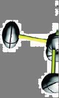


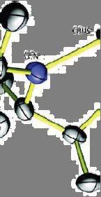

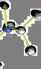

5 Cyclic amide tin (II) t-bu N Sn N Sn t-bu 13bi 1,3-bis(1,1-dimethylethyl)-4,5-dimethyl-(4R,5R)- 1 l) 45di l (4R 5R) 5/14 Picture o C 95.0 % o C 50.4 % ght (%) 1,3,2-diazastannolidin-2-ylidene (CAS # ) 25 0 TGA o C 1.7 % Wei - Sn-N distance is 2.02 Å - N-Sn-N angle is 82.7 o - Planar five-member ring *Dr. Adam S. Hock & Dr. Sang Bok Kim Temperature ( o C) - Clean evaporation w/o residue - Vapor pressure: 0.42 o C
6 ALD SnO 2 results 6/ x x10-2 Transmittance 4x10⁻² 3x10⁻² le) Resistivity ( cm) Reflectance 0.2 Deposition Rate (nm/cyc T & R Temperature ( o C) 2x Temperature ( o C) Wavelength (nm) - G/R: o C - Resistivity: ohm cm - Mobility: 7 cm 2 /V s - CC C.C: ~10 20 #/cm 3 - Transmittance: 87.8% - No C and N impurities J. Heo et al. Chem. Mater. 22, 4964 (2010).
7 Basic composite films properties 7/14 Growth rate Density Refractive index 0.18 data 0.17 rule of mixture Refractivee Index Density (g/cm 3 ) Growth rate (nm/cycle) Percentage of Al 2 O 3 subcycle Percentage of Al 2 O 3 subcycle Percentage of Al 2 O 3 Subcycle - G/R, film density, and refractive index deviates from the expected plot (rule of mixture) - Percentage of Al 2 O 3 subcycle ~20% ~50 at.% Al J. Heo et al. J. Phys. Chem. C 115, (2011).
8 Composition analysis (Sn,Al)O x - RBS 8/14 Energy (MeV) Al 300(1,0) 12(24,1) 30(9,1) 75(3,1) 60(3,2) 100 Rule of Mixture Measured (RBS) unit) concentration (at.%) (2,3) 400(0,1) Yi eld (arb. 0 Al C sub. O Al Sn Channel Percentage of Al 2 O 3 subcycle Rule of Mixture % Al 2 O 3 Al content (%) [ Al ] % Al O (100 % Al O ) ( Al 2 3 Sn : area density of cations per cycle, %( ): percentage of subcycle Higher Al concentration than expected over the entire range
9 Chemisorption analysis by RBS 9/ Al Al2 O SnO2 2.2 Average chemisorp ption rate TMA on CAT on Sn Al/(Sn+Al) from RBS (at.%) Al 2 O 3 subcycle: 1 Al 2 O 3 subcycle:2 60(3,2) Al 2 O 3 subcycle:3 60(2,3) Cycles 0.2 1) TMA -1 st : ~2.2 times enhancement on SnO 2-2 nd : Return to its own chemisorption 2) CAT -~5 cycles for full recovery J. Heo et al. J. Phys. Chem. C 115, (2011).
 Surface area: Smaller R rms 2) # of OH: SnO 2 :33 o Al 2 O 3 :47 o 3) Monolayer diffusion of Al? hness (nm) 0.5 0.")

10 What s happening? - TMA on SnO 2 10/ SnO 2 t: 100 nm 1) Surface area: Smaller R rms 2) # of OH: SnO 2 :33 o Al 2 O 3 :47 o 3) Monolayer diffusion of Al? hness (nm) Al 2 O (99,1) - ~2% Al Zalar rotation SnO 2 17nm r..m.s. roug Al/(Sn+Al) from RBS (at.%) O Concentration (%) nm μm μm μm μm m Sn Al ( 3) nm SnO 2 (Sn,Al)O x 7.9% Al Sputter time (min) - Tailing minor diffusion - Nanolaminate Al distribution
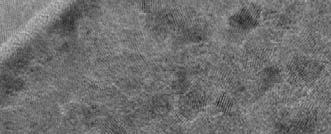
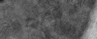
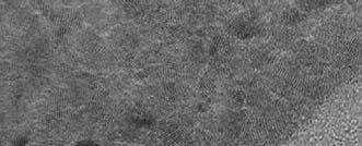
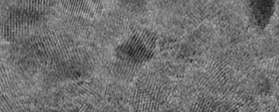
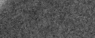
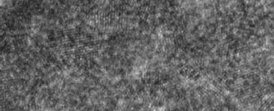
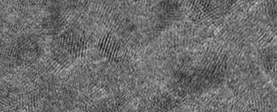
11 Si n 5 nm Polycrystalline SnO2 Si Polycrystalline Nanolaminate n 12(24,1) - 7.9% Al n Less crystallized Si 30(9,1) % Al Microstructure of composite films Si n Amorphous n 75(3,1) % Al 11/14
12 Electrical properties of composite films 12/ Vertical direction Lateral direction Low Al % anisotropic High Al % isotropic Vertical direction Vertical direction Lateral direction Lateral direction 10 0 Resistivity ( cm) Al/(Sn+Al) (at.%) - Electrical anisotropy - Less Al: nanolaminate distribution of resistive Al 2 O 3 - More Al: well mixed/ amorphous - Resistivity change over 15 orders of magnitude
13 Summary 13/14 # Macroscopic properties of (Sn,Al)O x composite films were studied. # Chemisorption behaviors govern films microstructures and electrical properties. # Nanolaminated Al distribution for small Al concentrations. ti # Controlled adjustment of film s electrical resistivity over more than 15 orders of magnitude was achieved.
Air")
 (3) Center for")
 - Group members - Dr.")
14 Acknowledgements 14/14 (1)Camille and Henry Dreyfus Postdoctoral Program (2)Air Force Office of Scientific Research (FA C-0075) (3) Center for Nanoscale Systems (NSF award no. ECS ) - Group members - Dr. Harish Bhandari - Dr. Sang Bok Kim
Low Temperature Atomic Layer Deposition of Tin Dioxide, SnO\(_2\)
") Low Temperature Atomic Layer Deposition of Tin Dioxide, \(_2\) The arvard community has made this article openly available. Please share how this access benefits you. Your story matters Citation eo, Jaeyeong,
Low Temperature Atomic Layer Deposition of Tin Dioxide, \(_2\) The arvard community has made this article openly available. Please share how this access benefits you. Your story matters Citation eo, Jaeyeong,
ALD of Manganese Silicate
 ALD of Manganese Silicate Roy G. Gordon, 1,2 * Lu Sun, 2 Qiang Chen, 3 Jin-Seong Park 4 and Sang Bok Kim 1 1 Department of Chemistry and Chemical Biology 2 School of Engineering and Applied Sciences, Cambridge,
Atomic layer epitaxy of rare earth oxide films on GaAs(111)A and their device properties
A and their device properties") Atomic layer epitaxy of rare earth oxide films on GaAs(111)A and their device properties Yiqun Liu 1)*, Min Xu 2), Jaeyeong Heo 1), Peide D. Ye 2), and Roy G. Gordon 1)** 1) Department of Chemistry and
Atomic layer epitaxy of rare earth oxide films on GaAs(111)A and their device properties Yiqun Liu 1)*, Min Xu 2), Jaeyeong Heo 1), Peide D. Ye 2), and Roy G. Gordon 1)** 1) Department of Chemistry and
ALD of Scandium Oxide from Tris(N,N -diisopropylacetamidinato)scandium and Water
scandium and Water") ALD of Scandium Oxide from Tris(N,N -diisopropylacetamidinato)scandium and Water Philippe P. de Rouffignac, Roy G. Gordon Dept. of Chemistry,, Cambridge, MA gordon@chemistry.harvard.edu (617) 495-4017
ALD of Scandium Oxide from Tris(N,N -diisopropylacetamidinato)scandium and Water Philippe P. de Rouffignac, Roy G. Gordon Dept. of Chemistry,, Cambridge, MA gordon@chemistry.harvard.edu (617) 495-4017
Effect of Volume Spray Rate on Highly Conducting Spray Deposited Fluorine Doped SnO2 Thin Films
 Effect of Volume Spray Rate on Highly Conducting Spray Deposited Fluorine Doped SnO2 Thin Films Dr.R.N. ARLE 1, B.L.KHATIK 2 1 Department of Physics, Jijamata College of Science and Arts, Bhende Bk.India
Nanoparticle generation using sputtering plasmas
 NCCAVS Joint Users Group Technical Symposium Nanomaterials for Energy, Biomedical, and Electronic Devices In Conjunction with the NCCAVS 35th Annual Equipment Exhibition Nanoparticle generation using sputtering
Nucleation and growth of nanostructures and films. Seongshik (Sean) Oh
 Oh") Nucleation and growth of nanostructures and films Seongshik (Sean) Oh Outline Introduction and Overview 1. Thermodynamics and Kinetics of thin film growth 2. Defects in films 3. Amorphous, Polycrystalline
Nucleation and growth of nanostructures and films Seongshik (Sean) Oh Outline Introduction and Overview 1. Thermodynamics and Kinetics of thin film growth 2. Defects in films 3. Amorphous, Polycrystalline
Characterization of Nanoscale Electrolytes for Solid Oxide Fuel Cell Membranes
 Characterization of Nanoscale Electrolytes for Solid Oxide Fuel Cell Membranes Cynthia N. Ginestra 1 Michael Shandalov 1 Ann F. Marshall 1 Changhyun Ko 2 Shriram Ramanathan 2 Paul C. McIntyre 1 1 Department
Study for double-layered AZO/ATO transparent conducting thin film
 Journal of Physics: Conference Series Study for double-layered AZO/ATO transparent conducting thin film To cite this article: Miaomiao Cao et al 2013 J. Phys.: Conf. Ser. 419 012022 View the article online
Effect of Doping Concentration on the Structural Properties of Zn: SnO 2
 IOSR Journal of Applied Physics (IOSR-JAP) e-issn: 2278-4861.Volume 7, Issue 3 Ver. II (May. - Jun. 2015), PP 45-49 www.iosrjournals.org Effect of Doping Concentration on the Structural Properties of Zn:
Precursors with Metal-Nitrogen Bonds for ALD of Metals, Nitrides and Oxides
 Precursors with Metal-Nitrogen Bonds for ALD of Metals, Nitrides and Oxides Abstract Roy Gordon Gordon@chemistry.harvard.edu, Cambridge, MA To achieve ALD s unique characteristics, ALD precursors must
High Rate Growth of SiO 2 by Thermal ALD Using Tris(dimethylamino)silane
silane") High Rate Growth of SiO 2 by Thermal ALD Using Tris(dimethylamino)silane and Ozone Guo Liu, Ritwik Bhatia, Eric W. Deguns, Mark J. Dalberth, Mark J. Sowa, Adam Bertuch, Laurent Lecordier, Ganesh Sundaram,
High Rate Growth of SiO 2 by Thermal ALD Using Tris(dimethylamino)silane and Ozone Guo Liu, Ritwik Bhatia, Eric W. Deguns, Mark J. Dalberth, Mark J. Sowa, Adam Bertuch, Laurent Lecordier, Ganesh Sundaram,
Atomic Oxygen-Resistant, Static-Dissipative, Pinhole-Free Coatings for Spacecraft
 Physical Sciences Inc. VG10-109 Atomic Oxygen-Resistant, Static-Dissipative, Pinhole-Free Coatings for Spacecraft Michelle T. Schulberg, Robert H. Krech, Frederick S. Lauten Physical Sciences Inc. Roy
Make sure the exam paper has 9 pages total (including cover page)
") UNIVERSITY OF CALIFORNIA College of Engineering Department of Electrical Engineering and Computer Sciences Fall 2010 EE143 Midterm Exam #2 Family Name First name SID Signature Solution Make sure the exam
UNIVERSITY OF CALIFORNIA College of Engineering Department of Electrical Engineering and Computer Sciences Fall 2010 EE143 Midterm Exam #2 Family Name First name SID Signature Solution Make sure the exam
Surfaces and Interfaces of Transparent Conducting Oxides Andreas Klein
 Surfaces and Interfaces of Transparent Conducting Oxides Andreas Klein Technische Universität Darmstadt, Institute of Materials Science, Surface Science Division Transparent conducting oxides d R T high
Low temperature deposition of thin passivation layers by plasma ALD
 1 Low temperature deposition of thin passivation layers by plasma ALD Bernd Gruska, SENTECH Instruments GmbH, Germany 1. SENTECH in brief 2. Low temperature deposition processes 3. SENTECH SI ALD LL System
Deposited by Sputtering of Sn and SnO 2
 Journal of the Korean Ceramic Society Vol. 49, No. 5, pp. 448~453, 2012. http://dx.doi.org/10.4191/kcers.2012.49.5.448 Comparative Study of Nitrogen Incorporated SnO 2 Deposited by Sputtering of Sn and
Conductive Gas Barriers Prepared by Using Atomic Layer Deposition Technique
 Available online at www.sciencedirect.com Procedia Engineering 36 (2012 ) 562 570 IUMRS-ICA 2011 Conductive Gas Barriers Prepared by Using Atomic Layer Deposition Technique Chih-Chieh Yu*, Meng-Yen Tsai,
Microstructure of Electronic Materials. Amorphous materials. Single-Crystal Material. Professor N Cheung, U.C. Berkeley
 Microstructure of Electronic Materials Amorphous materials Single-Crystal Material 1 The Si Atom The Si Crystal diamond structure High-performance semiconductor devices require defect-free crystals 2 Crystallographic
Mn DOPED SnO2 Semiconducting Magnetic Thin Films Prepared by Spray Pyrolysis Method
 International Journal of Scientific & Engineering Research Volume 2, Issue 4, April-2011 1 Mn DOPED SnO2 Semiconducting Magnetic Thin Films Prepared by Spray Pyrolysis Method K.Vadivel, V.Arivazhagan,
Access to the published version may require subscription. Published with permission from: Institute of Physics
 http://uu.diva-portal.org This is an author produced version of a paper published in Journal of Physics, Conference Series. This paper has been peer-reviewed but does not include the final publisher proof-corrections
ISSN GANENDRA, Vol. V, No. 1. PREPARATION AND CHARACTERIZATION OF TRANSPARENT CONDUCTIVE ZnO THIN FILMS BY DC MAGNETRON SPUTTERING
 PREPARATION AND CHARACTERIZATION OF TRANSPARENT CONDUCTIVE ZnO THIN FILMS BY DC MAGNETRON SPUTTERING Sudjatmoko, Suryadi, Widdi Usada, Tono Wibowo, and Wirjoadi Centre for Research and Development of Advanced
High Transmittance Ti doped ITO Transparent Conducting Layer Applying to UV-LED. Y. H. Lin and C. Y. Liu
 High Transmittance Ti doped ITO Transparent Conducting Layer Applying to UV-LED Y. H. Lin and C. Y. Liu Department of Chemical Engineering and Materials Engineering, National Central University, Jhongli,
11:30 AM - C4.4 Chemical Vapor Deposition of Cobalt Nitride and Its Application as an Adhesion-enhancing Layer for Advanced Copper Interconnects
 2012-04-11 SYMPOSIUM C 11:30 AM - C4.4 Chemical Vapor Deposition of Cobalt Nitride and Its Application as an Adhesion-enhancing Layer for Advanced Copper Interconnects Jing Yang 1, Harish B. Bhandari 1,
Chapter 3 Silicon Device Fabrication Technology
 Chapter 3 Silicon Device Fabrication Technology Over 10 15 transistors (or 100,000 for every person in the world) are manufactured every year. VLSI (Very Large Scale Integration) ULSI (Ultra Large Scale
Department of Chemistry, University of California, Davis, California 95616, USA 2
 Enhance Solar Water Splitting Performance by Utilizing Near Infrared Radiation with Composite Films of Hematite and Rare Earth Doped Upconversion Materials Ming Zhang, 1 Yongjing Lin, 2 Thomas J. Mullen,
ALD and CVD of Copper-Based Metallization for. Microelectronic Fabrication. Department of Chemistry and Chemical Biology
 ALD and CVD of Copper-Based Metallization for Microelectronic Fabrication Yeung Au, Youbo Lin, Hoon Kim, Zhengwen Li, and Roy G. Gordon Department of Chemistry and Chemical Biology Harvard University Introduction
Applications of Successive Ionic Layer Adsorption and Reaction (SILAR) Technique for CZTS Thin Film Solar Cells
 Technique for CZTS Thin Film Solar Cells") NANO VISION An International Open Free Access, Peer Reviewed Research Journal www.nano-journal.org ISSN 2231-2579 (Print) ISSN 2319-7633 (Online) Abbr: Nano Vision. 2013, Vol.3(3): Pg.235-239 Applications
NANO VISION An International Open Free Access, Peer Reviewed Research Journal www.nano-journal.org ISSN 2231-2579 (Print) ISSN 2319-7633 (Online) Abbr: Nano Vision. 2013, Vol.3(3): Pg.235-239 Applications
An advantage of thin-film silicon solar cells is that they can be deposited on glass substrates and flexible substrates.
 ET3034TUx - 5.2.1 - Thin film silicon PV technology 1 Last week we have discussed the dominant PV technology in the current market, the PV technology based on c-si wafers. Now we will discuss a different
IC/MEMS Fabrication - Outline. Fabrication
 IC/MEMS Fabrication - Outline Fabrication overview Materials Wafer fabrication The Cycle: Deposition Lithography Etching Fabrication IC Fabrication Deposition Spin Casting PVD physical vapor deposition
ITO. Crystal structure: Cubic, space group Ia3 No. 206, ci80, a = nm, Z = 16
 ITO Indium tin oxide (ITO) is a ternary composition of indium, tin and oxygen in varying proportions. Depending on the oxygen content, it can either be described as a ceramic or alloy. Indium tin oxide
Band offset engineering in ZnSnN 2 -based heterojunction for low-cost solar cells
 Band offset engineering in ZnSnN 2 -based heterojunction for low-cost solar cells Kashif Javaid 1,2,3, Weihua Wu 1, Jun Wang 4, Junfeng Fang 1, Hongliang Zhang 1, Junhua Gao 1, Fei Zhuge 1, Lingyan Liang*,1,5
SnO 2 Thin Films Prepared by Sol Gel Method for Honeycomb Textured Silicon Solar Cells
 ROMANIAN JOURNAL OF INFORMATION SCIENCE AND TECHNOLOGY Volume 10, Number 1, 2007, 25 33 SnO 2 Thin Films Prepared by Sol Gel Method for Honeycomb Textured Silicon Solar Cells E. MANEA 1, E. BUDIANU 1,
ZnO-based Transparent Conductive Oxide Thin Films
 IEEE EDS Mini-colloquium WIMNACT 32 ZnO-based Transparent Conductive Oxide Thin Films Weijie SONG Ningbo Institute of Material Technology and Engineering, Chinese Academy of Sciences, Ningbo, P. R. China
Area-selective atomic layer deposition for self-aligned fabrication
 Area-selective atomic layer deposition for self-aligned fabrication Adrie Mackus Eindhoven University a.j.m.mackus@tue.nl Area-selective ALD for bottom-up processing Top-down Bottom-up Building technology
The growth of patterned ceramic thin films from polymer precursor solutions Göbel, Ole
 University of Groningen The growth of patterned ceramic thin films from polymer precursor solutions Göbel, Ole IMPORTANT NOTE: You are advised to consult the publisher's version (publisher's PDF) if you
Supporting Information for:
 Supporting Information for: Charge-Transfer through Ultrathin Film TiO 2 on n-si(111) Photoelectrodes: Experimental and Theoretical Investigation of Electric Field-Enhanced Transport with a Non-Aqueous
O2 Plasma Damage and Dielectric Recoveries to Patterned CDO Low-k Dielectrics
 O2 Plasma Damage and Dielectric Recoveries to Patterned CDO Low-k Dielectrics H. Huang 1, J. Bao 1, H. Shi 1, P. S. Ho 1, M L McSwiney 2, M D Goodner 2, M Moinpour 2, and G M Kloster 2 1 Laboratory for
Ceramic Processing Research
 Journal of Ceramic Processing Research. Vol. 10, No. 4, pp. 536~540 (009) J O U R N A L O F Ceramic Processing Research Electrical and optical properties of MgO films deposited on soda lime glass by a
ATOMIC LAYER DEPOSITION OF 2D TRANSITION METAL DICHALOGENIDES
 ATOMIC LAYER DEPOSITION OF 2D TRANSITION METAL DICHALOGENIDES Annelies Delabie, M. Caymax, B. Groven, M. Heyne, K. Haesevoets, J. Meersschaut, T. Nuytten, H. Bender, T. Conard, P. Verdonck, S. Van Elshocht,
Building new catalytic. plasma nanostructuring and large-scale synthesis of nanowires PlasmaLab
 Uros Cvelbar Jozef Stefan Institute, Slovenia Building new catalytic sensors and devices with plasma nanostructuring and large-scale synthesis of nanowires PlasmaLab F4-IJS Sensors - Measurements of neutrals
Supporting Information
 Electronic Supplementary Material (ESI) for Journal of Materials Chemistry A. This journal is The Royal Society of Chemistry 18 Supporting Information CVD-grown copper tungstate thin films for solar water
Application note. Coated wafer mapping using an Agilent Cary 7000 Universal Measurement Spectrophotometer (UMS) with Solids Autosampler
 with Solids Autosampler") Coated wafer mapping using an Agilent Cary 7000 Universal Measurement Spectrophotometer (UMS) with Solids Autosampler Application note Materials testing and research Authors Travis Burt, Farinaz Haq Agilent
Coated wafer mapping using an Agilent Cary 7000 Universal Measurement Spectrophotometer (UMS) with Solids Autosampler Application note Materials testing and research Authors Travis Burt, Farinaz Haq Agilent
About Cambridge NanoTech Atomic Layer Deposition (ALD) Selected Applications Manufacturing Considerations ALD Reactors Summary
 Selected Applications Manufacturing Considerations ALD Reactors Summary") About Cambridge NanoTech Atomic Layer Deposition (ALD) Selected Applications Manufacturing Considerations ALD Reactors Summary Founded in 2003 by Dr. Jill Becker Located in Cambridge, MA Grew directly
About Cambridge NanoTech Atomic Layer Deposition (ALD) Selected Applications Manufacturing Considerations ALD Reactors Summary Founded in 2003 by Dr. Jill Becker Located in Cambridge, MA Grew directly
Growth and Doping of SiC-Thin Films on Low-Stress, Amorphous Si 3 N 4 /Si Substrates for Robust Microelectromechanical Systems Applications
 Journal of ELECTRONIC MATERIALS, Vol. 31, No. 5, 2002 Special Issue Paper Growth and Doping of SiC-Thin Films on Low-Stress, Amorphous Si 3 N 4 /Si Substrates for Robust Microelectromechanical Systems
Hydrogen permeation barrier performa characterization of vapor deposited aluminum oxide films using coloratio oxide
 JAIST Reposi https://dspace.j Title Hydrogen permeation barrier performa characterization of vapor deposited aluminum oxide films using coloratio oxide Yamada-Takamura, Y.; Koch, F.; Maier Author(s) H.
WŝŽŶĞĞƌŝŶŐ > ĞdžƉĞƌŝĞŶĐĞ ƐŝŶĐĞ ϭϵϳϰ WŝĐŽƐƵŶ ^he > Ρ WͲƐĞƌŝĞƐ > ƐLJƐƚĞŵƐ ƌŝěőŝŷő ƚśğ ŐĂƉ ďğƚǁğğŷ ƌğɛğăƌđś ĂŶĚ ƉƌŽĚƵĐƟŽŶ d, &hdhz K& d,/e &/>D /^, Z
 The ALD Powerhouse Picosun Defining the future of ALD Picosun s history and background date back to the very beginning of the field of atomic layer deposition. ALD was invented in Finland in 1974 by Dr.
Summary and Scope for further study
 Chapter 6 Summary and Scope for further study 6.1 Summary of the present study Transparent electronics is an emerging science and technology field concentrated on fabricating invisible electronic circuits
MATERIALS. Silicon Wafers... J 04 J 01. MATERIALS / Inorganics & thin films guide
 J MATERIALS SUBSTRATES Silicon Wafers... J 04 J J 01 MATERIALS SUBSTRATES NEYCO has a complete range of crystal substrates for a wide variety of applications, including Semiconductor, Biotechnology, Nanotechnology,
Thin film solar cells
 Thin film solar cells pn junction: a:si cells heterojunction cells: CIGS-based CdTe-based 1 Amorphous Si large concentration of defects N T >10 16 cm -3 ( dangling bonds D +, D -, D o ) passivation of
Properties of Inclined Silicon Carbide Thin Films Deposited by Vacuum Thermal Evaporation
 182 Properties of Inclined Silicon Carbide Thin Films Deposited by Vacuum Thermal Evaporation Oday A. Hamadi, Khaled Z. Yahia, and Oday N. S. Jassim Abstract In this work, thermal evaporation system was
Progress in Roll-to-Roll Atomic Layer Deposition
 Progress in Roll-to-Roll Atomic Layer Deposition Council for Chemical Research Barrier Workshop Arlington, Virginia September 20, 2012 E. Dickey Lotus Applied Technology Outline ALD for barrier films ALD
In O :SnO THIN FILM GAS SENSOR FOR DETECTION OF NO AT
 I.J.S.N., VOL.8 (3) 2017: 453-460 ISSN 2229 6441 In O :SnO THIN FILM GAS SENSOR FOR DETECTION OF NO AT DIFFERENT OPERATION TEMPERATURES Bushra A. Hasan & Rusul M.Abdallah University of Baghdad, College
Ageing Resistance (12 years) of Hard and Oxidation Resistant SiBCN Coatings
 of Hard and Oxidation Resistant SiBCN Coatings") Ageing Resistance (12 years) of Hard and Oxidation Resistant SiBCN Coatings Jiri Houska Department of Physics and NTIS - European Centre of Excellence, University of West Bohemia, Czech Republic Acknowledgment
Ageing Resistance (12 years) of Hard and Oxidation Resistant SiBCN Coatings Jiri Houska Department of Physics and NTIS - European Centre of Excellence, University of West Bohemia, Czech Republic Acknowledgment
The Potential of Photovoltaics
 The Potential of Photovoltaics AIMCAL 2008 2008 Fall Conference Vacuum Web Coating Brent P. Nelson October 22, 2008 NREL is a national laboratory of the U.S. Department of Energy Office of Energy Efficiency
Synthesis and Characterization of DC Magnetron Sputtered ZnO Thin Films Under High Working Pressures
 Accepted Manuscript Synthesis and Characterization of DC Magnetron Sputtered ZnO Thin Films Under High Working Pressures M. Hezam, N. Tabet, A. Mekki PII: S0040-6090(10)00417-7 DOI: doi: 10.1016/j.tsf.2010.03.091
Characteristics of Hafnium-Aluminum-Oxide Thin Films Deposited by Using Atomic Layer Deposition with Various Aluminum Compositions
 Journal of the Korean Physical Society, Vol. 47, No. 3, September 2005, pp. 501 507 Characteristics of Hafnium-Aluminum-Oxide Thin Films Deposited by Using Atomic Layer Deposition with Various Aluminum
Compound semiconductor layers for optoelectronic and photovoltaic purposes
 Compound semiconductor layers for optoelectronic and photovoltaic purposes PhD Thesis Zsófia Baji Supervisor: Dr György Molnár Budapest University of Technology and Economics and Research Centre for Natural
The impact of atomic layer deposition technological parameters on optical properties and morphology of Al 2 O 3 thin films
 Optica Applicata, Vol. XLV, No. 4, 5 DOI:.577/oa54 The impact of atomic layer deposition technological parameters on optical properties and morphology of Al O 3 thin films LESZEK A. DOBRZAŃSKI, MAREK SZINDLER
Influence on Whiskers:
 Sn Corrosion and It s Influence on Whiskers: J.W.Osenbach 1, J. M. DeLucca, B.D. Potteiger, R.L.Shook, and F.A. Baiocchi Agere Systems, Allentown PA Voice: (610) 712-5469 e-mail: osenbach@agere.com 0 ECTC
Effect of Cu-doping on Urbach Energy and Dispersion Parameters of Cu:NiO Film deposited by CSP
 International Letters of Chemistry, Physics and Astronomy Online: 2015-03-25 ISSN: 2299-3843, Vol. 48, pp 138-145 doi:10.18052/www.scipress.com/ilcpa.48.138 2015 SciPress Ltd., Switzerland Effect of Cu-doping
The Effect of Interfacial Roughness on the Electrical Properties of Organic Thin Film Transistors with Anisotropic Dielectric Layer
 Mol. Cryst. Liq. Cryst., Vol. 476, pp. 157=[403] 163=[409], 2007 Copyright # Taylor & Francis Group, LLC ISSN: 1542-1406 print=1563-5287 online DOI: 10.1080/15421400701735673 The Effect of Interfacial
Most semiconductor devices contain at least one junction between p-type and n-type material. These p-n junctions are fundamental to the performance
 Ch. 5: p-n Junction Most semiconductor devices contain at least one junction between p-type and n-type material. These p-n junctions are fundamental to the performance of functions such as rectification,
DEPOSITION AND CHARACTERISTICS OF TANTALUM NITRIDE FILMS BY PLASMA ASSISTED ATOMIC LAYER DEPOSITION AS CU DIFFUSION BARRIER
 Mat. Res. Soc. Symp. Proc. Vol. 766 2003 Materials Research Society E3.22.1 DEPOSITION AND CHARACTERISTICS OF TANTALUM NITRIDE FILMS BY PLASMA ASSISTED ATOMIC LAYER DEPOSITION AS CU DIFFUSION BARRIER Kyoung-Il
ECE 440 Lecture 27 : Equilibrium P-N Junctions I Class Outline:
 ECE 440 Lecture 27 : Equilibrium P-N Junctions I Class Outline: Fabrication of p-n junctions Contact Potential Things you should know when you leave Key Questions What are the necessary steps to fabricate
Studies on temperature and thickness dependent electrical resistance and conductivity of SnO 2 thin films
 Available online atwwwscholarsresearchlibrarycom Archives of Applied Science Research, 2015, 7 (4):71-75 (http://scholarsresearchlibrarycom/archivehtml) ISSN 0975-508X CODEN (USA) AASRC9 Studies on temperature
THE PERFORMANCE OF INDIUM TIN OXIDE FILMS DEPOSITED ON PLASTIC SUBSTRATE APPLIED FOR SOLAR-CELL BUOY
 Journal of Marine Science and Technology, Vol. 18, No. 6, pp. 82-829 () 82 THE PERFORMANCE OF INDIUM TIN OXIDE FILMS DEPOSITED ON PLASTIC SUBSTRATE APPLIED FOR SOLAR-CELL BUOY Chien-Kun Wang*, Jyh-Jier
Supporting Information
 Supporting Information Distance Dependence of Plamson-Enhanced Photocurrent in Dye-Sensitized Solar Cells Stacey D. Standridge, George C. Schatz, and Joseph T. Hupp Department of Chemistry, Northwestern
Sputtered Zinc Oxide Films for Silicon Thin Film Solar Cells: Material Properties and Surface Texture
 Poster FVS Workshop 2002 Sputtered Zinc Oxide Films for Silicon Thin Film Solar Cells: Material Properties and Surface Texture Texture etching of sputtered ZnO:Al films has opened up a variety of possibilities
CHAPTER 5. DEPOSITION AND CHARACTERIZATION OF ZINC STANNATE (Zn 2 SnO 4 ) THIN FILMS
 THIN FILMS") 106 CHAPTER 5 DEPOSITION AND CHARACTERIZATION OF ZINC STANNATE (Zn 2 SnO 4 ) THIN FILMS 5.1 INTRODUCTION Post-transition-metal oxides and their alloys have unique physical properties. Despite their large
106 CHAPTER 5 DEPOSITION AND CHARACTERIZATION OF ZINC STANNATE (Zn 2 SnO 4 ) THIN FILMS 5.1 INTRODUCTION Post-transition-metal oxides and their alloys have unique physical properties. Despite their large
Supporting Information
 Supporting Information Experimental Methods Pt ALD. The precursor used for ALD was trimethyl-methylcyclopentadienyl-platinum(iv) (MeCpPtMe 3 ) (Strem Chemicals, 99%), which has been widely reported for
MAI (methylammonium iodide) was synthesized by reacting 50 ml hydriodic acid
 was synthesized by reacting 50 ml hydriodic acid") Electronic Supplementary Material (ESI) for Energy & Environmental Science. This journal is The Royal Society of Chemistry Electronic Supplementary Information Stable semi-transparent CH 3 NH 3 PbI 3 planar
Electronic Supplementary Material (ESI) for Energy & Environmental Science. This journal is The Royal Society of Chemistry Electronic Supplementary Information Stable semi-transparent CH 3 NH 3 PbI 3 planar
Influence of Annealing Temperature on the Properties of ITO Films Prepared by Electron Beam Evaporation and Ion-Assisted Deposition
 Kasetsart J. (Nat. Sci.) 42 : 362-366 (2008) Influence of Annealing Temperature on the Properties of ITO Films Prepared by Electron Beam Evaporation and Ion-Assisted Deposition Artorn Pokaipisit 1 *, Mati
Atomic Layer Deposition (ALD)
") Atomic Layer Deposition (ALD) ALD provides Uniform, controlled, conformal deposition of oxide, nitride, and metal thin films on a nanometer scale. ALD is a self limiting thin film deposition technique
Atomic Layer Deposition (ALD) ALD provides Uniform, controlled, conformal deposition of oxide, nitride, and metal thin films on a nanometer scale. ALD is a self limiting thin film deposition technique
The Improvement in Energy Efficiency Based on Nano-structure Materials
 International Workshop on 1iGO Science and Technology 2010 The Improvement in Energy Efficiency Based on Nanostructure Materials Chien Chon Chen Department of Energy and Resources, National United University,
Supplementary Figure S1 Crystal structure of the conducting filaments in sputtered SiO 2
 Supplementary Figure S1 Crystal structure of the conducting filaments in sputtered SiO 2 based devices. (a) TEM image of the conducting filament in a SiO 2 based memory device used for SAED analysis. (b)
Microstructure, morphology and their annealing behaviors of alumina films synthesized by ion beam assisted deposition
 Nuclear Instruments and Methods in Physics Research B 206 (2003) 357 361 www.elsevier.com/locate/nimb Microstructure, morphology and their annealing behaviors of alumina films synthesized by ion beam assisted
LOW TEMPERATURE GROWTH OF SMOOTH INDIUM TIN OXIDE FILMS BY ULTRAVIOLET ASSISTED PULSED LASER DEPOSITION
 Journal of Optoelectronics and Advanced Materials Vol. 4, No. 1, March 2002, p. 21-25 LOW TEMPERATURE GROWTH OF SMOOTH INDIUM TIN OXIDE FILMS BY ULTRAVIOLET ASSISTED PULSED LASER DEPOSITION V. Craciun,
Effect of annealing temperature on the electrical properties of HfAlO thin films. Chun Lia, Zhiwei Heb*
 International Forum on Energy, Environment and Sustainable Development (IFEESD 2016) Effect of annealing temperature on the electrical properties of HfAlO thin films Chun Lia, Zhiwei Heb* Department of
In situ spectroscopic ellipsometry as a versatile tool to study atomic layer deposition
 In situ spectroscopic ellipsometry as a versatile tool to study atomic layer deposition Erik Langereis Department of Applied Physics e.langereis@tue.nl http://www.phys.tue.nl/pmp Ellipsometry Workshop
Studying Effect of Mg Doping on the Structural Properties of Tin Oxide Thin Films Deposited by the Spray Pyrolysis Technique
 Studying Effect of Mg Doping on the Structural Properties of Tin Oxide Thin Films Deposited by the Spray Pyrolysis Technique Abdul Rahman Sakhta 1* Ahmad Khdro Ali Darwisho 3 1.MSc Student, Department
Metallization deposition and etching. Material mainly taken from Campbell, UCCS
 Metallization deposition and etching Material mainly taken from Campbell, UCCS Application Metallization is back-end processing Metals used are aluminum and copper Mainly involves deposition and etching,
Transparent oxides for selective contacts and passivation in heterojunction silicon solar cells
 Transparent oxides for selective contacts and passivation in heterojunction silicon solar cells Francesca Menchini Photovoltaic Technologies Laboratory, ENEA Casaccia LIMS 2018 17-18 maggio 2018 Outline
UNCORRECTED PROOF ARTICLE IN PRESS. 2 Grain boundary structures of atomic layer deposited TiN. 3 S. Li a, *, C.Q. Sun b, H.S.
 + model 1 Thin Solid Films xx (2005) xxx xxx www.elsevier.com/locate/tsf 2 Grain boundary structures of atomic layer deposited TiN 3 S. Li a, *, C.Q. Sun b, H.S. Park c 4 5 6 7 8 bstract a School of Materials
Effect Thickness and Temperature Annealing on Structural and Optical Proportion of CuInTe 2 Thin Film
 AASCIT Journal of Materials 2016; 2(1): 1-5 Published online February 24 2016 (http://www.aascit.org/journal/materials) Effect Thickness and Temperature Annealing on Structural and Optical Proportion of
Czochralski Crystal Growth
 Czochralski Crystal Growth Crystal Pulling Crystal Ingots Shaping and Polishing 300 mm wafer 1 2 Advantage of larger diameter wafers Wafer area larger Chip area larger 3 4 Large-Diameter Wafer Handling
Lecture Day 2 Deposition
 Deposition Lecture Day 2 Deposition PVD - Physical Vapor Deposition E-beam Evaporation Thermal Evaporation (wire feed vs boat) Sputtering CVD - Chemical Vapor Deposition PECVD LPCVD MVD ALD MBE Plating
Introduction Transparent conducting oxides (TCOs) are a class of materials with numerous applications. What is a transparent conducting
 are a class of materials with numerous applications. What is a transparent conducting") AZO The Replacement for ITO? With applications in electronic screens and displays, LEDs and solar cells, transparent conducting oxides (TCOs) are considered key materials for a range of sectors. These
AZO The Replacement for ITO? With applications in electronic screens and displays, LEDs and solar cells, transparent conducting oxides (TCOs) are considered key materials for a range of sectors. These
ALD TiO 2 coated Silicon Nanowires for Lithium Ion Battery Anodes with enhanced Cycling Stability and Coulombic Efficiency
 ALD TiO 2 coated Silicon Nanowires for Lithium Ion Battery Anodes with enhanced Cycling Stability and Coulombic Efficiency Elmira Memarzadeh Lotfabad a, Peter Kalisvaart a,*, Kai Cui b, Alireza Kohandehghan
Atomic Layer Deposition of Novel High Dielectric Constant Materials
 Atomic Layer Deposition of Novel High Dielectric Constant Materials Adam Kueltzo # & Julie Lam * Thornton Fractional North High School # and Maine East High School * August 2, 2007 University of Illinois
Continuous and R2R ALD for Coating of Polymer Webs
 Continuous and R2R ALD for Coating of Polymer Webs AIMCAL 2011 Web Coating Conference Dr. Mikko Söderlund Application Manager Cost of ownership [ /m 2 ] R2R ALD a paradigm change Large-area (batch) ALD
BAND GAP SHIFT AND OPTICAL CHARACTERIZATION OF PVA-CAPPED PbO THIN FILMS: EFFECT OF THERMAL ANNEALING
 Chalcogenide Letters Vol. 8, No. 3, March 211, p.163 17 BAND GAP SHIFT AND OPTICAL CHARACTERIZATION OF PVA-CAPPED PbO THIN FILMS: EFFECT OF THERMAL ANNEALING P.U. ASOGWA * Department of Physics and Astronomy,
Ceramic Processing Research
 Journal of Ceramic Processing Research. Vol. 9, No. 6, pp. 638~642 (2008) J O U R N A L O F Ceramic Processing Research Study of Ga-Doped ZnO films deposited on PET substrates by DC magnetron sputtering
Pulsed Nucleation Layer of Tungsten Nitride Barrier Film and its Application in DRAM and Logic Manufacturing
 Pulsed Nucleation Layer of Tungsten Nitride arrier Film and its Application in DRAM and Logic Manufacturing Kaihan Ashtiani, Josh Collins, Juwen Gao, Xinye Liu, Karl Levy Novellus Systems, Inc. 4 N. First
Enhanced moisture-barrier property and flexibility of zirconium oxide/polymer hybrid structures
 Korean J. Chem. Eng., 33(3), 1070-1074 (2016) DOI: 10.1007/s11814-015-0225-5 INVITED REVIEW PAPER pissn: 0256-1115 eissn: 1975-7220 Enhanced moisture-barrier property and flexibility of zirconium oxide/polymer
CHAPTER 4. SYNTHESIS OF ALUMINIUM SELENIDE (Al 2 Se 3 ) NANO PARTICLES, DEPOSITION AND CHARACTERIZATION
 NANO PARTICLES, DEPOSITION AND CHARACTERIZATION") 40 CHAPTER 4 SYNTHESIS OF ALUMINIUM SELENIDE (Al 2 Se 3 ) NANO PARTICLES, DEPOSITION AND CHARACTERIZATION 4.1 INTRODUCTION Aluminium selenide is the chemical compound Al 2 Se 3 and has been used as a precursor
40 CHAPTER 4 SYNTHESIS OF ALUMINIUM SELENIDE (Al 2 Se 3 ) NANO PARTICLES, DEPOSITION AND CHARACTERIZATION 4.1 INTRODUCTION Aluminium selenide is the chemical compound Al 2 Se 3 and has been used as a precursor
Hot-wire deposited intrinsic amorphous silicon
 3 Hot-wire deposited intrinsic amorphous silicon With the use of tantalum as filament material, it is possible to decrease the substrate temperature of hot-wire deposited intrinsic amorphous silicon, while
Characteristics of Cobalt Films Deposited by Using a Remote Plasma ALD Method with a CpCo(CO) 2 Precursor
 2 Precursor") Journal of the Korean Physical Society, Vol. 50, No. 4, April 2007, pp. 1141 1146 Characteristics of Cobalt Films Deposited by Using a Remote Plasma ALD Method with a CpCo(CO) 2 Precursor Keunwoo Lee,
Journal of the Korean Physical Society, Vol. 50, No. 4, April 2007, pp. 1141 1146 Characteristics of Cobalt Films Deposited by Using a Remote Plasma ALD Method with a CpCo(CO) 2 Precursor Keunwoo Lee,
SUPPLEMENTARY INFORMATION
 SUPPLEMENTARY INFORMATION doi:.38/nphoton..7 Supplementary Information On-chip optical isolation in monolithically integrated nonreciprocal optical resonators Lei Bi *, Juejun Hu, Peng Jiang, Dong Hun
Characterization and erosion of metal-containing carbon layers
 Characterization and erosion of metal-containing carbon layers Martin Balden Max-Planck-Institut für Plasmaphysik, EURATOM Association, D-85748 Garching, Germany Materials Research Division (MF) Outline