Large-area patterning by roller-based nanoimprint lithography
|
|
|
- Lionel Glenn
- 6 years ago
- Views:
Transcription
1 JOANNEUM RESEARCH Forschungsgesellschaft Institute MATERIALS, Weiz, Austria Large-area patterning by roller-based nanoimprint lithography Ursula Palfinger, Dieter Nees, Stephan Ruttloff, Markus Leitgeb, Maria Belegratis, Barbara Stadlober
 Processes Machinery Materials Prerequisites for residual-free")

2 Outline 2 Outline Motivation Small structures on large areas Technology Roll-to-roll Nanoimprinting (R2R NIL) Processes Machinery Materials Prerequisites for residual-free imprinting Applications Roller-based fabrication of highly resolved metal patterns by a combination of residual-free NIL and a subsequent lift-off for transparent conductive foils and product ID features Summary
3 Motivation 3 Small structures on large areas Superhydrophobicity Lotus effect Light management Architecture Antireflectivity Low friction Riblets Point-of-Care Diagnostics Structural Colours Camouflage, Attraction Where is highly resolved patterning on large areas interesting? Others: Transport Traffic Security Packaging Energy Harvesting Flexible electronics OFETs Adhesion Gecko-effect
 micro and nano 2) 2D 2.")
4 Motivation 4 Small structures on large areas Superhydrophobicity Lotus effect Light management Architecture Antireflectivity Low friction Riblets Point-of-Care Diagnostics Structural Colours Camouflage, Attraction How can we produce them? 1) micro and nano 2) 2D 2.5D 3) large flexible areas 4) industrial process Flexible electronics OFETs Adhesion Gecko-effect
5 Technology Working stamp Substrate, resist Nanoimprint lithography Fast + accurate method for structure transfer UV or thermal curing of resist Very versatile (geometries, structure size) 3 Contact, imprint 4 Curing: T, UV Release
 Stamp Imprint CD = 1.")
6 Technology 6 Nanoimprint lithography Fast + accurate method for structure transfer UV or thermal curing of resist Very versatile (geometries, structure size) Stamp Imprint CD = 1.6 µm

 Stamp Imprint CD")
7 Technology 7 Nanoimprint lithography Fast + accurate method for structure transfer UV or thermal curing of resist Very versatile (geometries, structure size) Stamp Imprint CD = 200 nm
8 Technology 8 Nanoimprint lithography Working stamp Substrate, resist Contact, imprint Curing: T, UV Critical issues Batch NIL (serial) - Master (pattern quality, roughness) - Control of adhesion between master and resist - Resist viscosity (filling) - Curing behavior (fast, low shrinkage) - Fabrication volumes and process time - Upscaling? Release


9 Technology 9 Roll-to-Roll Nanoimprint lithography Working stamp Substrate, resist Photoresin (structured and cured) Contact, imprint Curing: T, UV Photoresin (liquid) Shim on roller Release Substrate line pressure rubber-coated counter roller


10 Technology 10 Roll-to-Roll Nanoimprint lithography Max. web width = 250 mm Web speed = m/min Max. UV intensity = 200 W/cm Line pressure UV-NIL = 18 kn Line pressure HE = 100 kn
")
 Technology 11")


")
11 Low (<0,01) Throughput (m 2 /s) Medium (0,01-1) High (>1) Technology 11 Resolution and throughput of printing technologies 100 Gravure Offset Flexo Rotary screen 1 R2R Nanoimprint lithography Flat screen 10-2 R2R photolitho Inkjet R2R-vacuum 10-4 Laser ablation High Resolution (< 10 µm) Medium Resolution (10-50 µm) Low Resolution (> 50 µm) Minimum feature size (µm) Source: OE-A 2009, 3D-MM
12 Low (<0,01) Throughput (m 2 /s) Medium (0,01-1) High (>1) Technology 12 Resolution and throughput of printing technologies 100 Gravure Offset Flexo Rotary screen 1 R2R Nanoimprint lithography Flat screen 10-2 R2R photolitho Inkjet R2R-vacuum 10-4 Laser ablation High Resolution (< 10 µm) Medium Resolution (10-50 µm) Low Resolution (> 50 µm) Minimum feature size (µm) Source: OE-A 2009, 3D-MM


13 Application 13 Creation of highly resolved metal patterns in R2R environment metal residue-free imprint stuctured metal layer


14 Applications 14 Critical for residual-free imprint: PATTERN GEOMETRY Structure depth and resist thickness l : line width s : space width d : structure depth h o : initial resist film thickness for open patterns


15 Applications 15 Critical for residual-free imprint: RESIST FLOW BEHAVIOR Squeeze flow model Stefan s equation : p t : imprint time η : resist viscosity l : imprinted line width p : imprint pressure h r : residual resist film thickness h o : initial resist layer thickness For vanishing residual resist film thickness the imprint time approaches infinity... H. Schift, J. Vac. Sci. Technol. 2008


16 Applications 16 Critical for residual-free imprint: SURFACES VS. RESIST CHEMISTRY Spontaneous dewetting and balance of interfacial forces S = g Substrate/Shim (g Substrate/Resin + g ResinShim ) < 0 g X/Y : interfacial energy S: spreading coefficient SJ Choi, J. Colloid. Interface Sci. 2009


17 Applications 17 Critical for residual-free imprint: CHOICE OF RESIST UV-NIL resist for aqueous lift-off Monomer low viscosity water soluble monofunctional Acrylate Photoinitator e.g. Non-ionic surfactant e.g. η = 10 mpas polar rest group Tuning of interfacial energies 20 mn/m < g < 45 mn/m Auner, Palfinger et al, Organic Electronics,
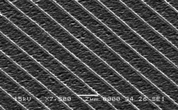
18 Applications 18 Residual-free R2R imprint SEM: top view SEM: cross section Zoom UV-Resist PET

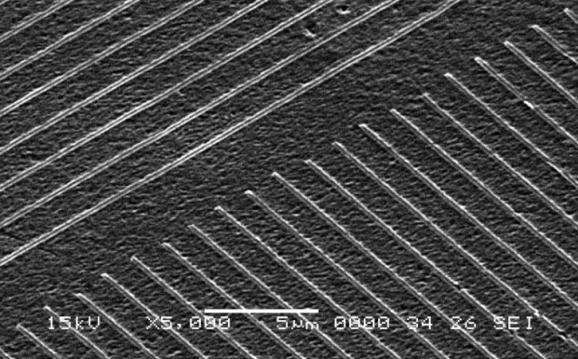
19 Applications 19 Residual-free R2R imprint SEM: top view SEM: cross section Zoom 1 metallization UV resist 2 water lift-off PET

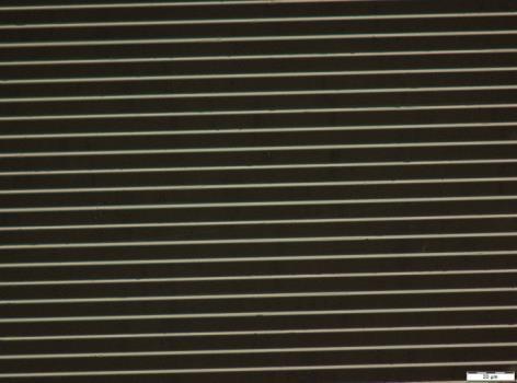
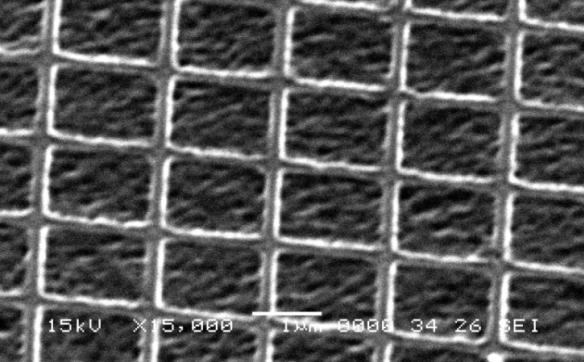
20 Applications 20 Al lines, CD = 1.6 µm 3 nm Cr + 30 nm Al Lift-off with H 2 O
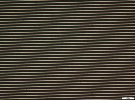
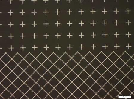
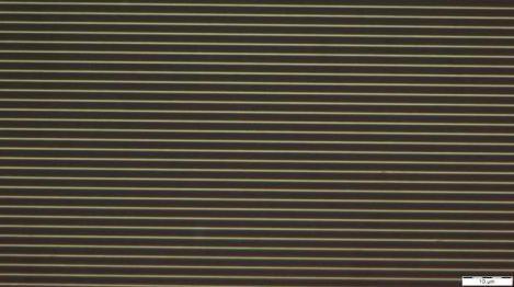
21 Applications 21 Al patterns, CD = 1.6 µm 21 web direction
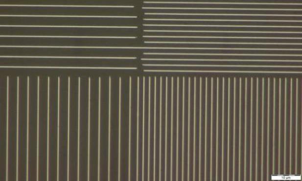
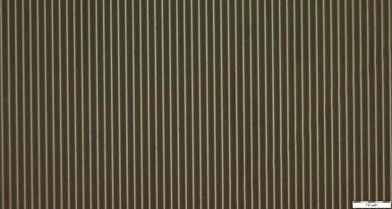
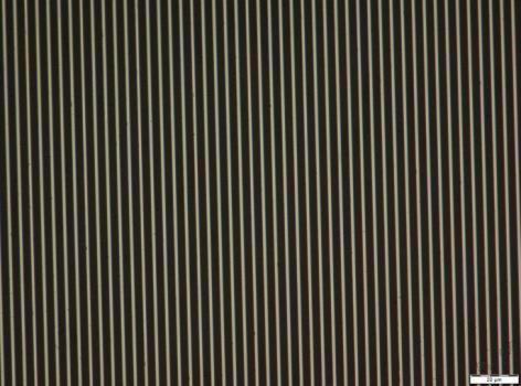
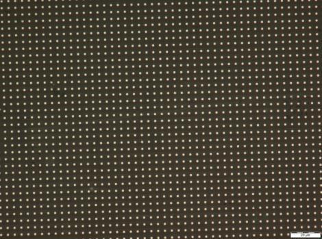
22 Applications 22 Al patterns, CD = 400 nm l/s = 1:4 web direction
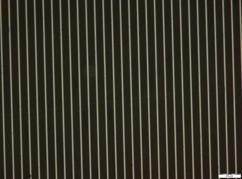
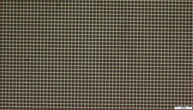
23 Applications 23 Application nano : Metal grids for transparent conductive foils SEM 400 nm


24 Applications 24 Application nano : Metal grids for transparent conductive foils SEM 400 nm Source: PolyIC Source: Samsung PyzoFlex technology Flexible displays, touch panels, sensor surfaces, shielding foils,
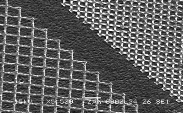
25 Applications 25 Application nano : Metal grids for transparent conductive foils SEM 200 nm
26 Summary 26 Summary Roller-based nanoimprinting is a large area, high resolution patterning process with very high potential. Residue-layer free R2R UV-NIL is possible, when pattern geometries and stamp and resin surface chemistry is optimized. We developed an acrylate-based imprint resin for water-based lift-off and used it for highly-resolved metal patterning on foil without the need of etching. Applications can be seen in electronics, optics, sensing, security features, shown examples: transparent conducting, packaging


27 Acknowledgements Dieter Nees Markus Leitgeb Herbert Gold Stephan Ruttloff Laco Kuna Volker Schmidt Maria Belegratis Barbara Stadlober


28 Lift-off in progress Thank you for your interest!
High Throughput Roll-to-Roll Production of Microfluidic Chips
 Proceedings High Throughput Roll-to-Roll Production of Microfluidic Chips Martin Smolka 1, *, Stephan Ruttloff 1, Dieter Nees 1, Christine Prietl 1, Valentin Satzinger 1, Bernhard Lamprecht 1, Philipp
Nanoimprinting in Polymers and Applications in Cell Studies. Albert F. YEE Chemical Engineering & Materials Science UC Irvine
 Nanoimprinting in Polymers and Applications in Cell Studies Albert F. YEE Chemical Engineering & Materials Science UC Irvine Presentation outline Motivation Reversal imprinting Soft inkpad imprinting on
Roll-to-Roll Nanoimprint - 6 회 -
 Roll-to-Roll Nanoimprint - 6 회 - 목차 Click to add Title 1 Roll to Roll nanoimprint Introduction : Continuous Production System (Roll-to-Roll) Fabrication Processes Fabrication of nano roll mold 2 Case study
MATERIALS technologies for industry
 MATERIALS technologies for industry JOANNEUM RESEARCH Professional innovation and technology provider Facts - Employees: 430 (2014) - Revenue: 38 M - Participations: K1 and K2 Centres, Nanotec Center Weiz,
Large Area Functional Surfaces By Roll-to-Roll Nanoimprint Lithography Project: APPOLO
 Large Area Functional Surfaces By Roll-to-Roll Nanoimprint Lithography Project: APPOLO Mr. Theodoros Tachtsidis Nanotypos 23rd and 24th of June Amsterdam Core Overview Nanotypos is a pioneering research
Surface Acoustic Wave fabrication using nanoimprint. Zachary J. Davis, Senior Consultant,
 Surface Acoustic Wave fabrication using nanoimprint Zachary J. Davis, Senior Consultant, zjd@teknologisk.dk Center for Microtechnology & Surface Analysis Micro and Nano Technology Sensor Technology Top
Processing guidelines
 Processing guidelines mr-uvcur21 series UV-curable Polymer for UV-based Nanoimprint Lithography Characteristics mr-uvcur21 is a liquid UV-curable polymer system with low viscosity and high curing rate
Technologies challenges and opportunities in UV and thermal Nanoimprint Lithography Roll2Roll technologies for flexible hybrid electronics
 Technologies challenges and opportunities in UV and thermal Nanoimprint Lithography Roll2Roll technologies for flexible hybrid electronics Thomas Kolbusch, Vice President, Coatema GmbH Wilfried Schipper,
LOW TEMPERATURE PHOTONIC SINTERING FOR PRINTED ELECTRONICS. Dr. Saad Ahmed XENON Corporation November 19, 2015
 LOW TEMPERATURE PHOTONIC SINTERING FOR PRINTED ELECTRONICS Dr. Saad Ahmed XENON Corporation November 19, 2015 Topics Introduction to Pulsed Light Photonic sintering for Printed Electronics R&D Tools for
Soft Lithography. Jin-Goo Park. Materials and Chemical Engineering Hanyang University, Ansan. Electronic Materials and Processing Lab.
 Hanyang University Soft Lithography Jin-Goo Park Materials and Chemical Engineering Hanyang University, Ansan Electronic Materials and Processing Lab. Introduction to Soft Lithography Research Micro- Electro-
Advanced Polymers And Resists For Nanoimprint Lithography
 Q U A L I T Y A S S U R A N C E MICROSYSTEMS & NANOSYSTEMS SPECIAL REPORT Advanced Polymers And Resists For Nanoimprint Lithography Numerous polymer systems specifically designed for nanoimprint lithography
Applications of Nano Patterning Process 1. Patterned Media
 Applications of Nano Patterning Process 1. Patterned Media Contents Introduction Part. 1. Nanoimprinting on Glass Substrate for Patterned Media Part. 2. Nanoinjection Molding of Nanopillars for Patterned
Innovative Roll-to-Roll Equipment & Material Development Suite
 Innovative Roll-to-Roll Equipment & Material Development Suite For Next Generation Technology from Carpe Diem Technologies and the University of Massachusetts Amherst By John Berg, Dimitur Benchev, James
Laser material processing for a wide range of applications
 Laser material processing for a wide range of applications Paul Hartmann Wien, 29.10.2018 www.joanneum.at/materials 2 Outline 1. Intro: Institute MATERIALS 2. Laser Production Technologies with multi-kw
Metallic Antireflection Structures Made from Silver Ink by a Liquid Transfer Imprint Lithography Technique
 Journal of Photopolymer Science and Technology Volume 30, Number 5 (2017) 539-544 C 2017SPST Metallic Antireflection Structures Made from Silver Ink by a Liquid Transfer Imprint Lithography Technique Ichiro
Three-dimensional SU-8 structures by reversal UV imprint
 Three-dimensional SU-8 structures by reversal UV imprint W. Hu, a B. Yang, C. Peng, and S. W. Pang b Solid State Electronics Laboratory, Department of Electrical Engineering and Computer Science, The University
Manipulation and control of spatial ALD layers for flexible devices. Aimcal Memphis 2016; Edward Clerkx
 Manipulation and control of spatial ALD layers for flexible devices Meyer Burger Netherlands Equipment manufacturer Functional inkjet printing Based in Eindhoven, the Netherlands Part of world-wide Meyer
Simple UV-based Soft-lithography Process for. Fabrication of Low-Loss Polymer PSQ-L-based. Waveguides
 Simple UV-based Soft-lithography Process for Fabrication of Low-Loss Polymer PSQ-L-based Waveguides Jie Teng 1, 2, 4, Stijn Scheerlinck 4, Geert Morthier 4, Roel Baets 4, Hongbo Zhang 2,3, Xigao Jian 2,3,
Polymer-based Microfabrication
 Polymer-based Microfabrication PDMS SU-8 PMMA Hydrogel 1 Soft Lithography Developed by Whitesides, et. al A set of techniques for microfabrication based on the use of lithography, soft substrate materials
A Novel Extrusion Microns Embossing Method of Polymer Film
 Modern Mechanical Engineering, 2012, 2, 35-40 http://dx.doi.org/10.4236/mme.2012.22005 Published Online May 2012 (http://www.scirp.org/journal/mme) A Novel Extrusion Microns Embossing Method of Polymer
WP7 JRA2 JRA2 Research on High Precision Manufacturing. Investigation of optimum NIL stamp fabrication method to copy sub-10 nm BCP features
 DELIVERABLE REPORT WP7 JRA2 JRA2 Research on High Precision Manufacturing D7.1 Investigation of optimum NIL stamp fabrication method to copy sub-10 nm BCP features M18 NFFA-Europe has received funding
AIMCAL R2R Conference
 Contents Introduction Markets OLED Structures Technology Fabrication Process Evaluation (Microstructure & etc) Summary Introduction [Merit of Rigid OLED Display] Cheap product cost Mass production Free
Superionic Solid State Stamping (S4)
") Superionic Solid State Stamping (S4) Lead Faculty Researcher: Placid Ferreira Department: Materials Science & Engineering Hsu et al, Nano Letters, 2007 1. Description: This dry, single step, electrochemical
Superionic Solid State Stamping (S4) Lead Faculty Researcher: Placid Ferreira Department: Materials Science & Engineering Hsu et al, Nano Letters, 2007 1. Description: This dry, single step, electrochemical
Holographix LLC Overview. High quality custom replicated optics and surface relief patterns in production volumes
 Holographix LLC Overview 2018 High quality custom replicated optics and surface relief patterns in production volumes One location in Marlborough, MA. 15,000 sq. ft. facility with additional space available
THE INNOVATION COMPANY MATERIALS. Institute for Surface Technologies and Photonics
 THE INNOVATION COMPANY MATERIALS Institute for Surface Technologies and Photonics Contact JOANNEUM RESEARCH Forschungsgesellschaft mbh MATERIALS Institute for Surface Technologies and Photonics Franz-Pichler-Strasse
Introduction to Nanoscience and Nanotechnology
 Introduction to Nanoscience and Nanotechnology ENS 463 2. Principles of Nano-Lithography by Alexander M. Zaitsev alexander.zaitsev@csi.cuny.edu Tel: 718 982 2812 Office 4N101b 1 Lithographic patterning
Choi, Jun-Hyuk Korea Institute of Machinery & Materials
 The 11 th US-Korea Nanosymposium Choi, Jun-Hyuk 2014. 09. 29 Korea Institute of Machinery & Materials About KIMM Nano-research Bldg Clean RM Five Research Divisions; 1. Advanced Manufacturing Sys. 2. Extreme
DPN 5000 System. Figure 1: The DPN 5000 System. Page 1 of 5. Created on 9/9/2011 Revision
 Introduction NanoInk s is a dedicated, versatile instrument capable of nanopatterning a variety of materials with nanoscale accuracy and precision. With NanoInk s proprietary MEMs devices and deposition
Printing Technologies for Flexible Electronics
 Printing Technologies for Flexible Electronics Thomas Walther Steinemann Technology AG, St. Gallen A view of a small Swiss mechanical engineering company into the market for printed electronics. Plastic
Fabrication of sub-100nm thick Nanoporous silica thin films
 Fabrication of sub-100nm thick Nanoporous silica thin films Abstract M. Ojha, W. Cho, J. L. Plawsky, W. N. Gill Department of chemical and biological engineering, Rensselaer Polytechnic Institute Low refractive
Vertically aligned Ni magnetic nanowires fabricated by diblock-copolymer-directed Al thin film anodization
 Vertically aligned Ni magnetic nanowires fabricated by diblock-copolymer-directed Al thin film anodization Researcher: Kunbae (Kevin) Noh, Graduate Student, MAE Dept. and CMRR Collaborators: Leon Chen,
Creating Greater Capacity on Smaller Spaces
 Creating Greater Capacity on Smaller Spaces Manufacturability of Pattern Media Babak Heidari, Obducat, Sweden Obducat Overview Company Background Founded in 1989 Facilities in Sweden (HQ) and in Cambridge
Thermal Nanoimprinting Basics
 Thermal Nanoimprinting Basics Nanoimprinting is a way to replicate nanoscale features on one surface into another, like stamping copies are made by traditional fabrication techniques (optical/ebeam lith)
types of curing mechanisms and developmental examples will be described in the following.
 transfer pattern. Increasingly, efforts are being made in many institutions to apply the technique to the processes for semiconductor devices [7, 8, 9, 10], storage media [11, 12], optical devices [13],
micro resist technology
 Characteristics Processing guidelines Negative Tone Photoresist Series ma-n 1400 ma-n 1400 is a negative tone photoresist series designed for the use in microelectronics and microsystems. The resists are
Roll-to-roll Vacuum Processing of Organic Thin Film Transistors
 Roll-to-roll Vacuum Processing of Organic Thin Film Transistors Hazel Assender Department of Materials University of Oxford DALMATIAN TECHNOLOGY 1 Aim of the Research To demonstrate the ability to fabricate
Towards scalable fabrication of high efficiency polymer solar cells
 Towards scalable fabrication of high efficiency polymer solar cells Hui Joon Park 2*, Myung-Gyu Kang 1**, Se Hyun Ahn 3, Moon Kyu Kang 1, and L. Jay Guo 1,2,3 1 Department of Electrical Engineering and
Seminar Micro- and Nano-technology
 Seminar Micro- and Nano-technology Seminar 1 Schedule Wednesday 17:45-18:30 Yannick Bourgin yannick.bourgin@uni-jena.de Phone: +49(3641)947990 www.iap.uni-jena.de Presentations 2 Presentation by 2 students
è Coating technologies and coating plant concepts for thin film liquid coating layers
 è Coating technologies and coating plant concepts for thin film liquid coating layers Andrea Glawe Technical Sales 1 Source: plastic electronics 22nd IFATCC-Congress Stresa 2010 www.coatema.de Outline
Advances in Intense Pulsed Light Solutions For Display Manufacturing. XENON Corporation Dr. Saad Ahmed Japan IDW 2016
 Advances in Intense Pulsed Light Solutions For Display Manufacturing XENON Corporation Dr. Saad Ahmed Japan IDW 2016 Talk Outline Introduction to Pulsed Light Applications in Display UV Curing Applications
Fabrication characteristics of a line-and-space pattern and a dot pattern on a roll mold by using electron-beam lithography
 0123456789 Bulletin of the JSME Journal of Advanced Mechanical Design, Systems, and Manufacturing Vol.10, No.5, 2016 Fabrication characteristics of a line-and-space pattern and a dot pattern on a roll
Continuous and R2R ALD for Coating of Polymer Webs
 Continuous and R2R ALD for Coating of Polymer Webs AIMCAL 2011 Web Coating Conference Dr. Mikko Söderlund Application Manager Cost of ownership [ /m 2 ] R2R ALD a paradigm change Large-area (batch) ALD
Efficient organic distributed feedback lasers with active films imprinted by thermal nanoimprint lithography
 Efficient organic distributed feedback lasers with active films imprinted by thermal nanoimprint lithography bidali zenuenean, ondo dago. Efficient organic distributed feedback lasers with active films
SCIENCE CHINA Technological Sciences. Replication of large area nanoimprint stamp with small critical dimension loss
 SCIENCE CHINA Technological Sciences RESEARCH PAPER March 2012 Vol.55 No.3: 600 605 doi: 10.1007/s11431-011-4695-3 Replication of large area nanoimprint stamp with small critical dimension loss MENG FanTao
Supplementary Figure 1. Schematic for the growth of high-quality uniform
 Supplementary Figure 1. Schematic for the growth of high-quality uniform monolayer WS 2 by ambient-pressure CVD. Supplementary Figure 2. Schematic structures of the initial state (IS) and the final state
Polymer-based optical interconnects using nano-imprint lithography
 Polymer-based optical interconnects using nano-imprint lithography Arjen Boersma,Sjoukje Wiegersma Bert Jan Offrein, Jeroen Duis, Jos Delis, Markus Ortsiefer, Geert van Steenberge, MikkoKarppinen, Alfons
High-Speed Roll-to-Roll Nanoimprint Lithography on Flexible Plastic Substrates**
 COMMUNICATION DOI: 10.1002/adma.200702650 High-Speed Roll-to-Roll Nanoimprint Lithography on Flexible Plastic Substrates** By Se Hyun Ahn and L. Jay Guo* The ability of micro- to nanometer-scale patterning
Nano-imprinting Lithography Technology І
 Nano-imprinting Lithography Technology І Agenda Limitation of photolithograph - Remind of photolithography technology - What is diffraction - Diffraction limit Concept of nano-imprinting lithography Basic
Developing Enhanced Substrates for OLED SSL
 Developing Enhanced Substrates for OLED SSL DOE SSL R&D Manufacturing Workshop San Diego CA 7 May, 2014 Dr. W. Dennis Slafer MicroContinuum, Inc. 57 Smith Place Cambridge, MA 02138 www.microcontinuum.com
Supporting Information
 Supporting Information The adhesion circle: A new approach to better characterize directional gecko-inspired dry adhesives Yue Wang, Samuel Lehmann, Jinyou Shao and Dan Sameoto* Department of Mechanical
Liquid Optically Clear Adhesive for Display Applications
 Liquid Optically Clear Adhesive for Display Applications Daniel Lu, PhD Technical Director Henkel Corporation LOCTITE Liquid Optically Clear Adhesives (LOCA) Cover lens LOCA Touch sensor LOCA LCD 2 LOCA
Photonic Curing and Soldering
 Photonic Curing and Soldering Ultra-fast Fabrication of Printed Electronics AIPIA Conference, Utrecht November 19 th, 215 Rob Hendriks Research Engineer Presentation overview Introduction Photonic Curing
Proton beam fabrication of nickel stamps for nanoimprint lithography
 Nuclear Instruments and Methods in Physics Research B 231 (2005) 407 412 www.elsevier.com/locate/nimb Proton beam fabrication of nickel stamps for nanoimprint lithography K. Ansari *, P.G. Shao, J.A. van
Production and analysis of optical gratings and nanostructures created by laser based methods
 Summary of the Ph.D. thesis Production and analysis of optical gratings and nanostructures created by laser based methods Kiss Bálint Supervisor: Dr. Vass Csaba Research fellow Doctoral School in Physics
Tau Series Configure your digital future
 EN Tau Series Configure your digital future 80 Years Experience Innovation Sustainability Durst. Advanced Digital Production Technology Durst. Advanced Digital Production Technology Durst is a world-leading
Module 12: Nano Imprint Lithography. Lecture 16: Nano Imprint Lithography 1
 Module 12: Nano Imprint Lithography Lecture 16: Nano Imprint Lithography 1 1 In the previous five lectures (Lectures 11 to 15) we have seen how Photolithography can be used for patterning, particularly
Sub-5 nm Structures Process Development and Fabrication Over Large Areas
 A S Jugessur,, 2017, 1:1 SciFed Nanotech Research Letters Research Article Open Access Sub-5 nm Structures Process Development and Fabrication Over Large Areas * A S Jugessur * University of Iowa Microfabrication
Nanocoating close to the market
 Nanocoating close to the market Moritz Graf zu Eulenburg Introduction Market overview Overview of most important coating aspects Description of different coating systems Description of different drying
Study of the resist deformation in nanoimprint lithography
 Study of the resist deformation in nanoimprint lithography Yoshihiko Hirai, a) Masaki Fujiwara, Takahiro Okuno, and Yoshio Tanaka Department of Mechanical System Engineering, Graduate School of Engineering,
High Definition Selective Metallization for Printed Electronics
 High Definition Selective Metallization for Printed Electronics Wolfgang Decker VAST FILMS, Ltd. Outline Introduction of VAST FILMS What is Selective Metalization Range of Applications for Selective Metalization
Laser Micromachining of Bulk Substrates and Thin Films Celine Bansal
 Laser Micromachining of Bulk Substrates and Thin Films Celine Bansal Oxford Lasers Ltd Moorbrook Park Didcot, Oxfordshire, OX11 7HP Tel: +44 (0) 1235 810088 www.oxfordlasers.com Outline Oxford Lasers Importance
Flexible functional devices at mass production level with the FLEx R2R sald platform
 Flexible functional devices at mass production level with the FLEx R2R sald platform D. Spee, W. Boonen, D. Borsa and E. Clerkx Meyer Burger (Netherlands) B.V. Meyer Burger Introduction to sald Challenges
Polymer Microfabrication: Methods and Application
 Polymer Microfabrication: Methods and Application Institute for Applied Materials & Department of Microsystems Engineering (IMTEK) at University of Freiburg KIT University of the State of Baden-Wuerttemberg
Enabling new industries with high volume manufacturing: learnings from R2R processing in wearable and flexible displays
 Enabling new industries with high volume manufacturing: learnings from R2R processing in wearable and flexible displays Tobias Stolley, Technologist Applied Materials WEB Coating GmbH Industiral Technologies
MATERIALS. Silicon Wafers... J 04 J 01. MATERIALS / Inorganics & thin films guide
 J MATERIALS SUBSTRATES Silicon Wafers... J 04 J J 01 MATERIALS SUBSTRATES NEYCO has a complete range of crystal substrates for a wide variety of applications, including Semiconductor, Biotechnology, Nanotechnology,
TEGO RC Silicones It s all about knowing when to let go
 TEGO RC Silicones It s all about knowing when to let go TEGO RC Silicones TECHNOLOGY ADVANTAGES OF TEGO RC SILICONES Pressure sensitive labels, tapes as well as hygiene products are the most important
A novel pick-and-place process for ultra-thin chips on flexible smart systems Thomas Meissner (Hahn-Schickard)
") A novel pick-and-place process for ultra-thin chips on flexible smart systems Thomas Meissner (Hahn-Schickard) Dr. rer. nat. Outline 1. Introduction to Hahn-Schickard 2. Motivation 3. Pick process 4. Application
A novel pick-and-place process for ultra-thin chips on flexible smart systems Thomas Meissner (Hahn-Schickard) Dr. rer. nat. Outline 1. Introduction to Hahn-Schickard 2. Motivation 3. Pick process 4. Application
Coatings and potting compounds for LED applications capabilities, limitations and trouble shooting
 Coatings and potting compounds for LED applications capabilities, limitations and trouble shooting Content Some theory on conformal coatings and potting compounds Conformal coatings for lighting applications
HIGH-THROUGHPUT, CONTINUOUS NANOPATTERNING TECHNOLOGIES FOR DISPLAY AND ENERGY APPLICATIONS
 HIGH-THROUGHPUT, CONTINUOUS NANOPATTERNING TECHNOLOGIES FOR DISPLAY AND ENERGY APPLICATIONS by Se Hyun Ahn A dissertation submitted in partial fulfillment of the requirements for the degree of Doctor of
THIN METALLIC LAYERS STRUCTURED BY E-BEAM LITHOGRAPHY. Miroslav HORÁČEK, Vladimír KOLAŘÍK, Michal URBÁNEK, František MATĚJKA, Milan MATĚJKA
 THIN METALLIC LAYERS STRUCTURED BY E-BEAM LITHOGRAPHY Miroslav HORÁČEK, Vladimír KOLAŘÍK, Michal URBÁNEK, František MATĚJKA, Milan MATĚJKA Ústav přístrojové techniky AV ČR, v. v. i., Královopolská 147,
micro resist technology
 Characteristics Processing guidelines Negative Tone Photoresist Series ma-n 2400 ma-n 2400 is a negative tone photoresist series designed for the use in micro- and nanoelectronics. The resists are available
Synthesis of diamond-like carbon films with super-low friction and wear properties
 Synthesis of diamond-like carbon films with super-low friction and wear properties MSE 676 All Things Carbon / 09-29-2009 A. Erdemir, O.L. Eryilmaz, and G. Fenske J. Vac. Sci. Technol. A 18(4), Jul/Aug
Perspectives for inline metrology introduction
 Perspectives for inline metrology introduction System selection and dimensioning strategies SURAGUS GmbH Efficient Testing Solutions SURAGUS GmbH Maria-Reiche-Str. 1 01109 Dresden Germany info@suragus.com
Multiphoton lithography based 3D micro/nano printing Dr Qin Hu
 Multiphoton lithography based 3D micro/nano printing Dr Qin Hu EPSRC Centre for Innovative Manufacturing in Additive Manufacturing University of Nottingham Multiphoton lithography Also known as direct
THIN FILM THICKNESS MEASUREMENT FOR EVALUATION OF RESIDUAL LAYER OF NANO-IMPRINT LITHOGRAPHY USING NEAR-FIELD OPTICS
 9 th INTERNATIONAL SYMPOSIUM ON MEASUREMENT AND QUALITY CONTROL (9 th ISMQC) November 21 24, 27, IIT Madras THIN FILM THICKNESS MEASUREMENT FOR EVALUATION OF RESIDUAL LAYER OF NANO-IMPRINT LITHOGRAPHY
10x Technology, LLC Bringing Advanced Materials to Life
 0x Technology, LLC Bringing Advanced Materials to Life Continuous R2R Coating Methodology to Manufacture Precision Microstructures for Displays, High-Brightness LEDs, Traffic Signs, Solar Concentrators
Photolithography I ( Part 2 )
") 1 Photolithography I ( Part 2 ) Chapter 13 : Semiconductor Manufacturing Technology by M. Quirk & J. Serda Bjørn-Ove Fimland, Department of Electronics and Telecommunication, Norwegian University of Science
1 Photolithography I ( Part 2 ) Chapter 13 : Semiconductor Manufacturing Technology by M. Quirk & J. Serda Bjørn-Ove Fimland, Department of Electronics and Telecommunication, Norwegian University of Science
Micro and nano structuring of carbon based materials for micro injection moulding and hot embossing
 Micro and nano structuring of carbon based materials for micro injection moulding and hot embossing Victor Usov, Graham Cross, Neal O Hara, Declan Scanlan, Sander Paulen, Chris de Ruijter, Daniel Vlasveld,
Micro & nanofabrica,on
 Micro & nanofabrica,on Photolitography : - contact - projec,on Electron Beam lithography (EBL) Nano imprint lithography Etching Contact Photolithography Substrate (e.g. Silicon wafer) Photoresist spinning
Impact of Zinc Oxide on the UV Absorbance and Mechanical Properties of UV Cured Films
 Impact of Zinc Oxide on the UV Absorbance and Mechanical Properties of UV Cured Films R. K. SONI, MEENU TEOTIA* Department of Chemistry C.C.S, University, Meerut Ultraviolet radiation [UVR] UVR is divided
LASER ABLATION AND NANOIMPRINT LITHOGRAPHY FOR THE FABRICATION OF EMBEDDED LIGHT REDIRECTING MICROMIRRORS
 LASER ABLATION AND NANOIMPRINT LITHOGRAPHY FOR THE FABRICATION OF EMBEDDED LIGHT REDIRECTING MICROMIRRORS A. Kostro 1, M. A. Gonzalez Lazo 2, Y. Leterrier 2, E. Siringil 3, P. Hoffmann 3, A. M. Schüler
ABSTRACT: INTRODUCTION:
 ABSTRACT: Nano-Composite Polymer Optical Coatings Tom Faris Vampire Optical Coatings, Inc. P.O. Box 240 Kirkersville, Ohio 43033 (740)-927-5257 f(740)-927-5032 vampirecoatings@earthlink.net Traditionally
Supplementary Information
 Supplementary Information 13.2% efficiency Si nanowire/pedot:pss hybrid solar cell using a transferimprinted Au mesh electrode Kwang-Tae Park 1 *, Han-Jung Kim 1 *, Min-Joon Park 2, Jun-Ho Jeong 1,3, Jihye
NanoSystemsEngineering: NanoNose Final Status, March 2011
 1 NanoSystemsEngineering: NanoNose Final Status, March 2011 The Nanonose project is based on four research projects (VCSELs, 3D nanolithography, coatings and system integration). Below, the major achievements
Polymer Microfabrication (Part II) Prof. Tianhong Cui, Mechanical Engineering ME 8254
 Prof. Tianhong Cui, Mechanical Engineering ME 8254") Polymer Microfabrication (Part II) Prof. Tianhong Cui, Mechanical Engineering ME 8254 Other Polymer Techniques Embossing Low cost High throughput Structures as small as 25 nm Injection molding Features
Polymer Microfabrication (Part II) Prof. Tianhong Cui, Mechanical Engineering ME 8254 Other Polymer Techniques Embossing Low cost High throughput Structures as small as 25 nm Injection molding Features
Modeling the mechanical deformation of nickel foils for nanoimprint lithography on double-curved surfaces
 Downloaded from orbit.dtu.dk on: Apr 21, 2018 Modeling the mechanical deformation of nickel foils for nanoimprint lithography on double-curved surfaces Sonne, Mads Rostgaard; Cech, Jiri; Hattel, Jesper
UV15: For Fabrication of Polymer Optical Waveguides
 CASE STUDY UV15: For Fabrication of Polymer Optical Waveguides Master Bond Inc. 154 Hobart Street, Hackensack, NJ 07601 USA Phone +1.201.343.8983 Fax +1.201.343.2132 main@masterbond.com CASE STUDY UV15:
Achieving premium product appeal. Metasheen Superior mirror and liquid metal effects
 Achieving premium product appeal Metasheen Superior mirror and liquid metal effects Agenda Metasheen at a glance Performance highlights Our global portfolio Guide formulations 2 Metasheen at a glance Metasheen
Supporting Information. Low Temperature Oxidation-free Selective Laser Sintering of Cu
 Supporting Information Low Temperature Oxidation-free Selective Laser Sintering of Cu Nanoparticle Paste on a Polymer Substrate for the Flexible Touch Panel Applications Jinhyeong Kwon 1,, Hyunmin Cho
Latest development of energy curable resin for high performance easy-to-clean hardcoats
 Latest development of energy curable resin for high performance easy-to-clean hardcoats Ph. De Groote, M. Hutchins, A. Chen, S. Cappelle, M. Kanouni, J. Zhang Functional Coatings Conference, June 5 & 6,
3M Electrically Conductive Double-Sided Tape 9711S Series
 Technical Data August 2017 3M Electrically Conductive Double-Sided Tape 9711S Series Product Description 3M Electrically Conductive Double-Sided Tape 9711S Series contains XYZ electrically conductive pressure
Supporting Information
 Copyright WILEY-VCH Verlag GmbH & Co. KGaA, 69469 Weinheim, Germany, 2013. Supporting Information for Adv. Mater., DOI: 10.1002/adma.201300794 Highly Stretchable Patterned Gold Electrodes Made of Au Nanosheets
纳米压印技术最新进展. Obducat Technologies AB., Sweden Gang Luo,
 纳米压印技术最新进展 Obducat Technologies AB., Sweden Gang Luo, 20170711 History 2016 Launch of SINDRE Large Area 2015 Acquire Solarsemi Gmbh 2015 Awarded by NNT for Pioneering NIL into production 2014 Launch and
Step and Flash Imprint Lithography for sub-100nm Patterning
 Step and Flash Imprint Lithography for sub-100nm Patterning Matthew Colburn, Annette Grot, Marie Amistoso, Byung Jin Choi, Todd Bailey, John Ekerdt, S.V. Sreenivasan, James Hollenhorst, C. Grant Willson
Fabrication Technology, Part I
 EEL5225: Principles of MEMS Transducers (Fall 2003) Fabrication Technology, Part I Agenda: Oxidation, layer deposition (last lecture) Lithography Pattern Transfer (etching) Impurity Doping Reading: Senturia,
Figure 6. Rare-gas atom-beam diffraction patterns. These results were obtained by Wieland Schöllkopf and Peter Toennies at the Max-Planck Institute
 Figure 6. Rare-gas atom-beam diffraction patterns. These results were obtained by Wieland Schöllkopf and Peter Toennies at the Max-Planck Institute in Göttingen, Germany, using a freestanding, 100nm-period
Vacuum Deposition of High Performance Gas Barrier Materials for Electronics Applications
 Vacuum Deposition of High Performance Gas Barrier Materials for Electronics Applications Hélène Suttle DPhil Research Student Department of Materials -University of Oxford AIMCAL Fall Conference October
Inkjet printing of oxide thin films and nanoparticles with potential use for anti-counterfeiting films and patterns
 1 Inkjet printing of oxide thin films and nanoparticles with potential use for anti-counterfeiting films and patterns M. Vilardell, V.R. Vlad, X. Sintas, A. Calleja Oxolutia S.L., Edifici Eureka, PRUAB,
NANOMETER AND HIGH ASPECT RATIO PATTERNING BY ELECTRON BEAM LITHOGRAPHY USING A SIMPLE DUV NEGATIVE TONE RESIST
 NANOMETER AND HIGH ASPECT RATIO PATTERNING BY ELECTRON BEAM LITHOGRAPHY USING A SIMPLE DUV NEGATIVE TONE RESIST H. Elsner and H.-G. Meyer Institute for Physical High Technology (IPHT), Dept. of Cryoelectronics,
Development of Imprint Materials for the Step and Flash Imprint Lithography Process
 Development of Imprint Materials for the Step and Flash Imprint Lithography Process Frank Xu a, Nick Stacey b, Michael Watts a, Van Truskett a, Ian McMackin a, Jin Choi a, Philip Schumaker a, Ecron Thompson