Rapid Cleaning Using Novel Processes With Coa7ngs
|
|
|
- Mark Eaton
- 6 years ago
- Views:
Transcription
1 Rapid Cleaning Using Novel Processes With Coa7ngs Alex Brewer and John Moore Daetec, LLC 1227 Flynn Rd., Unit 310 Camarillo CA Surface PreparaHon and Cleaning Conference April SPCC Santa Clara California 1


2 Washable Coa7ngs Coa7ngs that Clean CoatsCleans TM emulsify PR Washable Primers lih off/ protect from metal X-linking Washable Coa7ngs/Adhesives Laser processing Temporary bonding Dicing and polishing Planarizing FF Tape Washable Safe 2016 SPCC Santa Clara California 2
 to Clean Solids (Polymers) Solvent Immersion Long Time Ineffec7ve Corrosion Solvent Intensive Hazardous Coats/Cleans TM Using")
3 CoatsCleans TM vs. Immersion Treated Wafers Using Liquids (Solvents) to Clean Solids (Polymers) Solvent Immersion Long Time Ineffec7ve Corrosion Solvent Intensive Hazardous Coats/Cleans TM Using Solids (Polymers) to Clean Solids (Polymers) Treated Wafers Coat & Water Wash Fast Mul7-purpose Metal Safe Water Rinse EHS Approved 2016 SPCC Santa Clara California 3
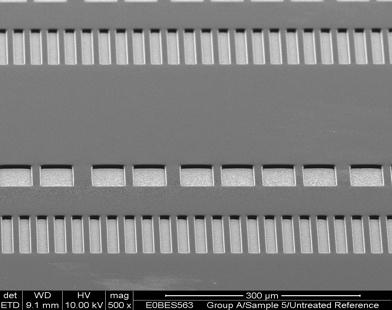
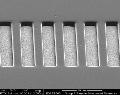
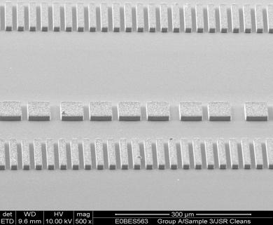

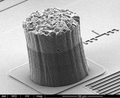
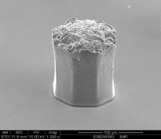
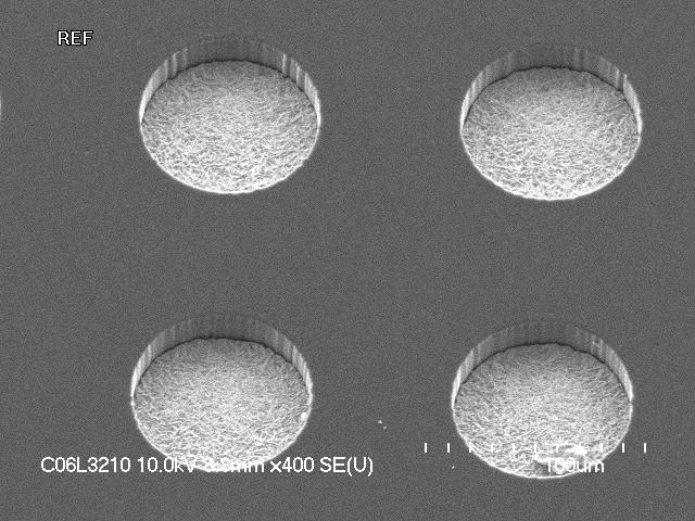
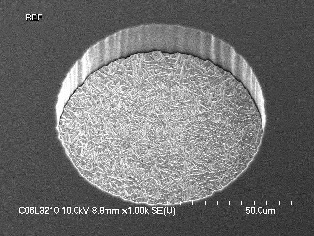
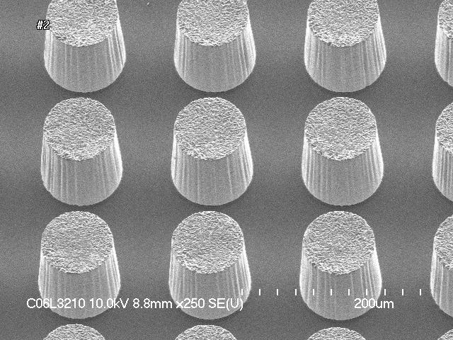
4 Stripping Neg-Acrylic PR (Bumping) Coats/Cleans PR PR Heat/Emulsify Coating Wafer ID Before PR Present 1 Pos - Liq Merck AZ P um Wafer ID A2er <15min Dissolve/Rinse 5 Neg - DF TOK um 3 Neg - Liq DOW BPR um 6 Neg - DF Asahi Sunfort um Before PR Present A2er <15min Dissolve/Rinse 4 Neg-DF DuPont WB100-series um 2 Neg - Liq JSR THB-151N 20-24um H2O Rinse 2016 SPCC Santa Clara California 4
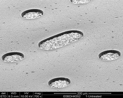
5 Washable Primer - Eliminates Residue Adhesive Adhesive Temperature (C) Process Cleans on Rubber Coa=ng + Washable Primer Wafer Cleans, temperature monitor during rota=on Stripping DIW Rinsing Current (amps) 1.00E E E E-04 Dry Clean Substrate Hg-Probe Surface Measurement on Co, Following Treatment Solvent + Rinse Coat Solvent 50 Rinsing, Drying 2.00E-04 Not Clean Time (sec) 0.00E Voltage 2016 SPCC Santa Clara California 5

6 Improved Thermal Resistance Thermal Resistance Chemical funchonality Phenyl Polyester [ DaeCoat TM Systems Phenyl silicones Polyphenylsulfones Salt conjugates [ 2016 SPCC Santa Clara California 6


7 Thermal Resistant Washable Coa7ngs Thermal Exposure AUer RT Water Rinse PVA PVP DaeCoat TM PVA PVP DaeCoat TM 200C 250C 300C 2016 SPCC Santa Clara California 7
8 Ex.: Wafer Temporary Bonding Process Demand Objec7ve: Wafer thinning, backside processing Mechanical (e.g. grind): Yes Thermal resistance: <300C Process/chemicals: Yes Uniformity: ~2um Recommenda7on DaeCoat TM 355 Green solvent washable, DaeClean TM 300 Broad chemical resistance Thermal resistance: >300C Carrier: Solid, due to small die, simple release/cleans chemical diffusion recycled 2016 SPCC Santa Clara California 8


9 Thinning, Processing, Release Grinding, backside processing, singula7on Singula7on offers 1-2mm channel between devices to enable simple debond & wash 2016 SPCC Santa Clara California 9


10 Green Solvent Wash Adhesive DaeClean TM 300 Device: Capture/Further Processing DaeClean TM 300 Immersion Adhesive Dissolu7on Carrier Release/Recycle 2016 SPCC Santa Clara California 10
11 Ex.: Device Temporary Bonding Process Demand Objec7ve: LTCC flip-chip bond & encapsulate Mechanical (e.g. grind): No Thermal resistance: ~275C Process/chemicals: limited, RT flux cleaner Uniformity: <10% Recommenda7on DaeCoat TM 535 Hot DIW washable RT chemical resistance Thermal resistance: >300C Carrier: Porous chemical diffusion recycled 2016 SPCC Santa Clara California 11


12 LTCC/HTCC Microelectronics on a ceramic substrate MulH-layer packaging MEMS, military, RF, wireless Thickness <50um to >250um Commonly um Green tape several suppliers Extremely fragile handling challenge 2016 SPCC Santa Clara California 12


13 DIW Wash Adhesive (LTCC) UV tape film Chemical Safe Hot DIW Wash (<80C) Film Frame Akach to device front-side Porous Carrier Debond UV Debond Pick & Place 2016 SPCC Santa Clara California 13
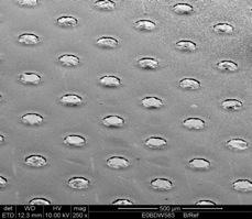
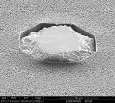
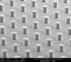
14 Ex.: Wafer Planariza7on Process Demand Objec7ve: Wafer planarizing coahng for backside processing Mechanical (e.g. grind): No Thermal resistance: <300C Process/chemicals: Yes Uniformity: <5% Special: Desire to finish on FF tape Recommenda7on DaeCoat TM 357 Green solvent washable, DaeClean TM 300 Broad chemical resistance Thermal resistance: >300C Carrier: desire FF tape Safe for DaeClean TM SPCC Santa Clara California 14


15 Washable Planariza7on Coa7ng Sputtering Test Sputter deposition of 200nm Ti:W + 300nm Copper on 250µm thick PCA DaeCoat TM 357 using LLS802 multi target tool wafer with 100:1 mix ratio after sputtering wafer with 50:1 mix ratio after sputtering Chamber Capability: 24 x 4-6 wafers per batch 8 x 8 wafers per batch 4 x 300 mm wafers per batch 2016 SPCC Santa Clara California 15
16 Parameter CoaHng Thickness DaeCoat TM 355 DaeCoat TM 357 DaeCoat TM 515 DaeCoat TM 535 DaeCoat TM 615 <5-100 um <5-250 um <5-100 um <5-60 um <5-60 um Cure UV/Thermal UV/Thermal Thermal Thermal Thermal Max temp ~300C ~300C ~300C ~300C ~200C ApplicaHon Resists RT DIW* Resists Acids* Resists Litho Stripper Chemistries* Clean CondiHons Temp Bonding or CoaHng DaeClean TM 300 (Safe Solvent) Temp Planarizing CoaHng DaeClean TM 300 (Safe Solvent) Laser Processing RT DIW Temp Bonding or CoaHng 80C, DIW Temp Bonding or CoaHng DaeClean TM 150 (Detergent) 2016 SPCC Santa Clara California 16
Optical Profilometry of Substrate Bow Reduction Using Temporary Adhesives
 Optical Profilometry of Substrate Bow Reduction Using Temporary Adhesives a Paul Flynn and b John Moore a FRT of America, LLC 1101 South Winchester Blvd., Suite L-240, San Jose, CA 95128 408-261-2632,
Challenges for Embedded Device Technologies for Package Level Integration
 Challenges for Embedded Device Technologies for Package Level Integration Kevin Cannon, Steve Riches Tribus-D Ltd Guangbin Dou, Andrew Holmes Imperial College London Embedded Die Technology IMAPS-UK/NMI
TSV Processing and Wafer Stacking. Kathy Cook and Maggie Zoberbier, 3D Business Development
 TSV Processing and Wafer Stacking Kathy Cook and Maggie Zoberbier, 3D Business Development Outline Why 3D Integration? TSV Process Variations Lithography Process Results Stacking Technology Wafer Bonding
Sheet) Graphite Sheet
 Graphite Sheet") PGS(Pyrolytic Graphite Sheet) Graphite Sheet Panasonic Electronic Device Co.,Ltd Panasonic Electronic Device Hokkaido Co.,Ltd PGS Graphite Sheet PGS (Pyrolytic Highly Oriented Graphite Sheet) is made of
PGS(Pyrolytic Graphite Sheet) Graphite Sheet Panasonic Electronic Device Co.,Ltd Panasonic Electronic Device Hokkaido Co.,Ltd PGS Graphite Sheet PGS (Pyrolytic Highly Oriented Graphite Sheet) is made of
Thin Wafers Bonding & Processing
 Thin Wafers Bonding & Processing A market perspective 2012 Why New Handling Technologies Consumer electronics is today a big driver for smaller, higher performing & lower cost device configurations. These
Chips Face-up Panelization Approach For Fan-out Packaging
 Chips Face-up Panelization Approach For Fan-out Packaging Oct. 15, 2015 B. Rogers, D. Sanchez, C. Bishop, C. Sandstrom, C. Scanlan, TOlson T. REV A Background on FOWLP Fan-Out Wafer Level Packaging o Chips
Illuminating Innovations
 Illuminating Innovations TM Silicone Solutions for LED Packaging Emir Debastiani Application Engineer Dow Corning Brazil Email: emir.debastiani@dowcorning.com Table of Contents Dow Corning Introduction
Novel Materials and Activities for Next Generation Package. Hitachi Chemical., Co.Ltd. Packaging Solution Center Hiroaki Miyajima
 Novel Materials and Activities for Next Generation Package Hitachi Chemical., Co.Ltd. Packaging Solution Center Hiroaki Miyajima 1. Activities of Packaging Solution Center 2. Novel Materials for Next Gen.
Fraunhofer IZM Bump Bonding and Electronic Packaging
 Fraunhofer IZM Bump Bonding and Electronic Packaging Fraunhofer Institute for Reliability and Microintegration (IZM) Gustav-Meyer-Allee 25 13355 Berlin Germany Dipl.-Ing. Thomas Fritzsch Contact: thomas.fritzsch@izm.fraunhofer.de
MEPTEC Semiconductor Packaging Technology Symposium
 MEPTEC Semiconductor Packaging Technology Symposium Advanced Packaging s Interconnect Technology Process Shift and Direction October 23, 2014 Jay Hayes- Director of Business Development -Bumping and Flip
Wafer Level Molded DDFN Package Project Duane Wilcoxen
 Wafer Level Molded DDFN Package Project Duane Wilcoxen Definition of DDFN (Encapsulated CSP) DDFN package basically is a CSP device with an epoxy coating on all (or most) of the device sides for added
Hot Chips: Stacking Tutorial
 Hot Chips: Stacking Tutorial Choon Lee Technology HQ, Amkor Enabling a Microelectronic World Mobile Phone Technology Change Feature Phone Smartphone Smartphones as a Percentage of All Phones Source : The
Low-temperature, Simple and Fast Integration Technique of Microfluidic Chips by using a UV-curable Adhesive
 Low-temperature, Simple and Fast Integration Technique of Microfluidic Chips by using a UV-curable Adhesive Supplementary Information Channel fabrication Glass microchannels. A borosilicate glass wafer
Recent Advances in Die Attach Film
 Recent Advances in Die Attach Film Frederick Lo, Maurice Leblon, Richard Amigh, and Kevin Chung. AI Technology, Inc. 70 Washington Road, Princeton Junction, NJ 08550 www.aitechnology.com Abstract: The
Die Attach Materials. Die Attach G, TECH. 2U. TECHNICAL R&D DIV.
 Die Attach Materials Die Attach G, TECH. 2U. TECHNICAL R&D DIV. 2 Topics 3 What it is X 5,000 X 10,000 X 50,000 Si Chip Au Plating Substrate Ag Resin 4 Current Products Characteristics H9890-6A H9890-6S
Enabling Materials Technology for Multi-Die Integration
 Enabling Materials Technology for Multi-Die Integration Dr. Jeffrey M. Calvert Global R&D Director, Advanced Packaging Technologies Dow Electronic Materials 455 Forest St., Marlborough, MA 01752 USA jcalvert@dow.com
RELIABILITY AND PERFORMANCE OF THERMALLY CONDUCTIVE ADHESIVES. Scott T. Allen Henkel Corporation Irvine, CA, USA
 RELIABILITY AND PERFORMANCE OF THERMALLY CONDUCTIVE ADHESIVES Scott T. Allen Henkel Corporation Irvine, CA, USA scott.t.allen@us.henkel.com Slide page 1 Introduction Increasing Device Performance Drives
3M Thermally Conductive Adhesive Tape 8940
 Product Information Sheet 15. Oct 2004 Supersedes Version 01. Mai 2004 Product Description 3M TM Thermally Conductive Adhesive Tape 8940 is designed to provide an efficient heat transfer path between heat
IME Technical Proposal. High Density FOWLP for Mobile Applications. 22 April High Density FOWLP Consortium Forum
 IME Technical Proposal High Density FOWLP for Mobile Applications 22 April 2014 Packaging driver for portable / mobile applications Key drivers/needs Smaller form-factor lower profile, substrate-less Higher
3 Thermally Conductive Tapes
 3 Thermally Conductive Tapes Technical Data July, 21 Product Description 3M Thermally Conductive Tapes 885, 881, and 8815 are designed to provide a preferential heat-transfer path between heat-generating
Ultra Fine Pitch Bumping Using e-ni/au and Sn Lift-Off Processes
 Ultra Fine Pitch Bumping Using e-ni/au and Sn Lift-Off Processes Andrew Strandjord, Thorsten Teutsch, and Jing Li Pac Tech USA Packaging Technologies, Inc. Santa Clara, CA USA 95050 Thomas Oppert, and
Chapter 3 Silicon Device Fabrication Technology
 Chapter 3 Silicon Device Fabrication Technology Over 10 15 transistors (or 100,000 for every person in the world) are manufactured every year. VLSI (Very Large Scale Integration) ULSI (Ultra Large Scale
KGC SCIENTIFIC Making of a Chip
 KGC SCIENTIFIC www.kgcscientific.com Making of a Chip FROM THE SAND TO THE PACKAGE, A DIAGRAM TO UNDERSTAND HOW CPU IS MADE? Sand CPU CHAIN ANALYSIS OF SEMICONDUCTOR Material for manufacturing process
Mostafa Soliman, Ph.D. May 5 th 2014
 Mostafa Soliman, Ph.D. May 5 th 2014 Mostafa Soliman, Ph.D. 1 Basic MEMS Processes Front-End Processes Back-End Processes 2 Mostafa Soliman, Ph.D. Wafers Deposition Lithography Etch Chips 1- Si Substrate
Chapter 2 Manufacturing Process
 Digital Integrated Circuits A Design Perspective Chapter 2 Manufacturing Process 1 CMOS Process 2 CMOS Process (n-well) Both NMOS and PMOS must be built in the same silicon material. PMOS in n-well NMOS
TSV Interposer Process Flow with IME 300mm Facilities
 TSV Interposer Process Flow with IME 300mm Facilities Property of Institute of Microelectronics (IME)-Singapore August 17, 2012 Outline 1. TSV interposer (TSI) cross sectional schematic TSI with BEOL,
Platypus Gold Coated Substrates. Bringing Science to the Surface
 Platypus Gold Coated Substrates Bringing Science to the Surface Overview Gold Coated Substrates - Gold Coating Introduction - Glossary of Terms - Gold Coating Methods - Critical Features Platypus Gold
Dow Corning WL-5150 Photodefinable Spin-On Silicone
 Dow Corning WL-515 Photodefinable Spin-On Silicone Properties and Processing Procedures Introduction Dow Corning WL-515 is a silicone formulation which can be photopatterned and cured using standard microelectronics
Material based challenge and study of 2.1, 2.5 and 3D integration
 1 Material based challenge and study of 2.1, 2.5 and 3D integration Toshihisa Nonaka Packaging Solution Center R&D Headquarters Hitachi Chemical Co., Ltd., Sep. 8, 2016 Hitachi Chemical Co., Ltd. 2010.
3D-IC Integration using D2C or D2W Alignment Schemes together with Local Oxide Reduction
 3D-IC Integration using D2C or D2W Alignment Schemes together with Local Oxide Reduction Gilbert Lecarpentier*, Jean-Stéphane Mottet* SET S.A.S. (Smart Equipment Technology), 131 Impasse Barteudet, 74490
Equipment and Process Challenges for the Advanced Packaging Landscape
 Equipment and Process Challenges for the Advanced Packaging Landscape Veeco Precision Surface Processing Laura Mauer June 2018 1 Copyright 2018 Veeco Instruments Inc. Outline» Advanced Packaging Market
Because of equipment availability, cost, and time, we will use aluminum as the top side conductor
 Because of equipment availability, cost, and time, we will use aluminum as the top side conductor Top Side Conductor vacuum deposition Aluminum sputter deposit in Argon plasma CVC 601-sputter deposition
Next Gen Packaging & Integration Panel
 Next Gen Packaging & Integration Panel ECTC 2012 Daniel Tracy, Sr. Director Industry Research & Statistics SEMI May 29, 2012 Packaging Supply Chain Market Trends Material Needs and Opportunities Market
Molding materials performances experimental study for the 3D interposer scheme
 Minapad 2014, May 21 22th, Grenoble; France Molding materials performances experimental study for the 3D interposer scheme Y. Sinquin, A. Garnier, M. Argoud, A. Jouve, L. Baud, J. Dechamp, N. Allouti,
Chapter 4 Fabrication Process of Silicon Carrier and. Gold-Gold Thermocompression Bonding
 Chapter 4 Fabrication Process of Silicon Carrier and Gold-Gold Thermocompression Bonding 4.1 Introduction As mentioned in chapter 2, the MEMs carrier is designed to integrate the micro-machined inductor
Coatings and potting compounds for LED applications capabilities, limitations and trouble shooting
 Coatings and potting compounds for LED applications capabilities, limitations and trouble shooting Content Some theory on conformal coatings and potting compounds Conformal coatings for lighting applications
PHYS 534 (Fall 2008) Process Integration OUTLINE. Examples of PROCESS FLOW SEQUENCES. >Surface-Micromachined Beam
 Process Integration OUTLINE. Examples of PROCESS FLOW SEQUENCES. >Surface-Micromachined Beam") PHYS 534 (Fall 2008) Process Integration Srikar Vengallatore, McGill University 1 OUTLINE Examples of PROCESS FLOW SEQUENCES >Semiconductor diode >Surface-Micromachined Beam Critical Issues in Process
PHYS 534 (Fall 2008) Process Integration Srikar Vengallatore, McGill University 1 OUTLINE Examples of PROCESS FLOW SEQUENCES >Semiconductor diode >Surface-Micromachined Beam Critical Issues in Process
Avatrel Stress Buffer Coatings: Low Stress Passivation and Redistribution Applications
 Avatrel Stress Buffer Coatings: Low Stress Passivation and Redistribution Applications Ed Elce, Chris Apanius, Jeff Krotine, Jim Sperk, Andrew Bell, Rob Shick* Sue Bidstrup-Allen, Paul Kohl Takashi Hirano,
Be careful what you wish for
 Be careful what you wish for Four Point Probe Key measurement tool in microelectronics fabrication What is Four Point Probing Four Point Probing is a method for measuring the resistivity of a substance.
3M Tapes for Solar Panel Fabrication. Bond with trust.
 3M Tapes for Solar Panel Fabrication Bond with trust. 2 3M Tapes for Solar Panel Fabrication How tomorrow s breakthroughs come together. Dependable, cost-effective assembly solutions from a world leader
Fabrication Technology, Part I
 EEL5225: Principles of MEMS Transducers (Fall 2003) Fabrication Technology, Part I Agenda: Oxidation, layer deposition (last lecture) Lithography Pattern Transfer (etching) Impurity Doping Reading: Senturia,
CMP for Thru-Silicon Vias TSV Overview & Examples March 2009
 CMP for Thru-Silicon Vias TSV Overview & Examples March 2009 Packaging Evolution Source: Yole Dev 2007 2 3D Integration Source: Yole Dev 2007 Growth rates for 3D integration Flash continues to drive the
3DIC Integration with TSV Current Progress and Future Outlook
 3DIC Integration with TSV Current Progress and Future Outlook Shan Gao, Dim-Lee Kwong Institute of Microelectronics, A*STAR (Agency for Science, Technology and Research) Singapore 9 September, 2010 1 Overview
The Solubility is the Solution. BELLAND Alkaline Soluble Polymers The Company, Applications and Environment
 The Solubility is the Solution BELLAND Alkaline Soluble Polymers The Company, Applications and Environment The Company The BellandTechnology AG specializes in the development and production of excellent
Ultralow Residue Semiconductor Grade Fluxes for Copper Pillar Flip-Chip
 Ultralow Residue Semiconductor Grade Fluxes for Copper Pillar Flip-Chip SzePei Lim (Presenter), Jason Chou, Maria Durham, and Dr. Andy Mackie Indium Corporation 1 Outline of Presentation Roadmaps and challenges
CERN/NA62 GigaTracKer Hybrid Module Manufacturing
 CERN/NA62 GigaTracKer Hybrid Module Manufacturing Fraunhofer Institute for Reliability and Microintegration Gustav-Meyer-Allee 25 13355 Berlin Germany Dipl.-Ing. Thomas Fritzsch Contact: Fraunhofer IZM
Fabrication Process. Crystal Growth Doping Deposition Patterning Lithography Oxidation Ion Implementation CONCORDIA VLSI DESIGN LAB
 Fabrication Process Crystal Growth Doping Deposition Patterning Lithography Oxidation Ion Implementation 1 Fabrication- CMOS Process Starting Material Preparation 1. Produce Metallurgical Grade Silicon
Removal of JSR THB-S375N Photoresist Using a Photoresist Stripper with an Improved EHS Profile Abstract Key words
 Removal of JSR THB-S375N Photoresist Using a Photoresist Stripper with an Improved EHS Profile Yuanmei Cao, Kimberly Pollard, Travis Acra, Nichelle Gilbert, Richie Peters, Donald Pfettscher Abstract Negative
HBLED packaging is becoming one of the new, high
 Ag plating in HBLED packaging improves reflectivity and lowers costs JONATHAN HARRIS, President, CMC Laboratories, Inc., Tempe, AZ Various types of Ag plating technology along with the advantages and limitations
Overview of CMP for TSV Applications. Robert L. Rhoades, Ph.D. Presentation for AVS Joint Meeting June 2013 San Jose, CA
 Overview of CMP for TSV Applications Robert L. Rhoades, Ph.D. Presentation for AVS Joint Meeting June 2013 San Jose, CA Outline TSV s and the Role of CMP TSV Pattern and Fill TSV Reveal (non-selective)
EE 5344 Introduction to MEMS. CHAPTER 3 Conventional Si Processing
 3. Conventional licon Processing Micromachining, Microfabrication. EE 5344 Introduction to MEMS CHAPTER 3 Conventional Processing Why silicon? Abundant, cheap, easy to process. licon planar Integrated
CYCLOTENE* 4000 Series Advanced Electronic Resins (Photo BCB)
") Revised: February 2005 CYCLOTENE* 4000 Series Advanced Electronic Resins (Photo BCB) Processing Procedures for CYCLOTENE 4000 Series Photo BCB Resins DS2100 Puddle Develop Process 1. Introduction The CYCLOTENE
Revised: February 2005 CYCLOTENE* 4000 Series Advanced Electronic Resins (Photo BCB) Processing Procedures for CYCLOTENE 4000 Series Photo BCB Resins DS2100 Puddle Develop Process 1. Introduction The CYCLOTENE
TECHNICAL DATA SHEET 1 P a g e Revised August, 2014
 1 P a g e Revised August, 2014 TAIYO PSR-4000 CC01SE (UL Name: PSR-4000JV / CA-40JV) LIQUID PHOTOIMAGEABLE CURTAIN COAT SOLDER MASK Curtain Coat Application Aqueous Developing Solder Mask RoHS Compliant
Introduction of CSC Pastes
 Introduction of CSC Pastes Smart Phones & Conductive Pastes Chip Varistors Chip Inductors LC Filters Flexible Printed Circuit Boards Electronic Molding Compounds ITO Electrodes PCB Through Holes Semiconductor
Electrical and Fluidic Microbumps and Interconnects for 3D-IC and Silicon Interposer
 Electrical and Fluidic Microbumps and Interconnects for 3D-IC and Silicon Interposer Li Zheng, Student Member, IEEE, and Muhannad S. Bakir, Senior Member, IEEE Georgia Institute of Technology Atlanta,
The Role of Wafer Bonding in 3D Integration and Packaging
 1 The Role of Bonding in 3D Integration and Packaging James Hermanowski and Greg George SUSS MicroTec, Inc. 228 Suss Drive Waterbury Center, VT 05677 2 The Role of Bonding in 3D Integration and Packaging
Challenges of Fan-Out WLP and Solution Alternatives John Almiranez
 Challenges of Fan-Out WLP and Solution Alternatives John Almiranez Advanced Packaging Business Development Asia Introduction to Fan-Out WLP Introduction World of mobile gadgetry continues to rapidly evolve
Extending product lifetime with ALD moisture barrier
 Whitepaper Extending product lifetime with ALD moisture barrier 01 executive summary Atomic Layer Deposition (ALD) is a thin film technology that enables new and highly competitive products. Typical applications
4411N 4411G 4412N 4412G
 Extreme Sealing Tape Technical Data October, 2011 Product Description 3M Extreme Sealing Tape is a family of single coated, pressure sensitive adhesive tapes designed for difficult sealing applications.
METHODS OF COATING FABRICATION
 METHODS OF COATING FABRICATION Zbigniew Grzesik http://home.agh.edu.pl/~grzesik Department of Physical Chemistry and Modelling DEFINITION The coating is the thin outer layer of the object, which physiochemical
Microelectronics. Integrated circuits. Introduction to the IC technology M.Rencz 11 September, Expected decrease in line width
 Microelectronics Introduction to the IC technology M.Rencz 11 September, 2002 9/16/02 1/37 Integrated circuits Development is controlled by the roadmaps. Self-fulfilling predictions for the tendencies
Nondestructive Internal Inspection. The World s Leading Acoustic Micro Imaging Lab
 Nondestructive Internal Inspection The World s Leading Acoustic Micro Imaging Lab Unmatched Capabilities and Extensive Expertise At Your Service SonoLab, a division of Sonoscan, is the world s largest
Photoresist Coat, Expose and Develop Laboratory Dr. Lynn Fuller
 ROCHESTER INSTITUTE OF TECHNOLOGY MICROELECTRONIC ENGINEERING Photoresist Coat, Expose and Develop Laboratory Dr. Lynn Fuller Webpage: http://www.rit.edu/lffeee 82 Lomb Memorial Drive Rochester, NY 14623-5604
IMPLEMENTATION OF A FULLY MOLDED FAN-OUT PACKAGING TECHNOLOGY
 IMPLEMENTATION OF A FULLY MOLDED FAN-OUT PACKAGING TECHNOLOGY B. Rogers, C. Scanlan, and T. Olson Deca Technologies, Inc. Tempe, AZ USA boyd.rogers@decatechnologies.com ABSTRACT Fan-Out Wafer-Level Packaging
Specialty Adhesives for Graphic Arts Applications SIGNS FRAMES GRAPHICS DISPLAYS
 Specialty Adhesives for Graphic Arts Applications SIGNS FRAMES DISPLAYS GRAPHICS SIGNS GRAPHICS FRAMES DISPLAYS LABELS IMAGE PLAQUES NAMEPLATES S capa North America is a world-class manufacturing operation
MCC. NANO PMMA and Copolymer
 MCC PRODUCT ATTRIBUTES NANO and Submicron linewidth control (polymethyl methacrylate) is a versatile polymeric material that is well suited Sub 0.1µm imaging for many imaging and non-imaging microelectronic
9 rue Alfred Kastler - BP Nantes Cedex 3 - France Phone : +33 (0) website :
 website :") 9 rue Alfred Kastler - BP 10748-44307 Nantes Cedex 3 - France Phone : +33 (0) 240 180 916 - email : info@systemplus.fr - website : www.systemplus.fr November 2010 - Version 2 Written by: Sylvain HALLEREAU
9 rue Alfred Kastler - BP 10748-44307 Nantes Cedex 3 - France Phone : +33 (0) 240 180 916 - email : info@systemplus.fr - website : www.systemplus.fr November 2010 - Version 2 Written by: Sylvain HALLEREAU
Miniaturized electronic packaging for wearable health monitors
 Miniaturized electronic packaging for wearable health monitors Jayna Sheats Terepac Corporation, Waterloo, Ontario, Canada Market needs Technology needs What Terepac does to address both 2013 MEPTEC Medical
Hybrid BARC approaches for FEOL and BEOL integration
 Hybrid BARC approaches for FEOL and BEOL integration Willie Perez a, Stephen Turner a, Nick Brakensiek a, Lynne Mills b, Larry Wilson b, Paul Popa b a Brewer Science, Inc., 241 Brewer Dr., Rolla, MO 6541
Solid State Sensors. Microfabrication 8/22/08 and 8/25/08
 Solid State Sensors Microfabrication 8/22/08 and 8/25/08 Purpose of This Material To introduce the student to microfabrication techniques as used to fabricate MEMS Sensors Understand concepts not specifics
Novel Polysulfide Substrates for Flexible Electronics. Tolis Voutsas, Ph.D. VP, Business Development Ares Materials, Inc.
 Novel Polysulfide Substrates for Flexible Electronics Tolis Voutsas, Ph.D. VP, Business Development Ares Materials, Inc. Contents 6/21/2017 2 Company overview Founded 2014, spin-out of the University of
The ABC s of CMP for DWB and SOI. Robert L. Rhoades, Ph.D. CAMP Conference Presentation August 9, 2010
 The ABC s of CMP for DWB and SOI Robert L. Rhoades, Ph.D. CAMP Conference Presentation August 9, 2010 Outline Introduction Direct Wafer Bonding (DWB) Background CMP for DWB Silicon-On-Insulator (SOI) Background
Bulk MEMS Fabrication Details Dr. Lynn Fuller, Casey Gonta, Patsy Cadareanu
 ROCHESTER INSTITUTE OF TECHNOLOGY MICROELECTRONIC ENGINEERING Bulk MEMS Fabrication Details Dr. Lynn Fuller, Casey Gonta, Patsy Cadareanu Webpage: http://people.rit.edu/lffeee 82 Lomb Memorial Drive Rochester,
Microelectronic Materials. Catalog
 Microelectronic Materials Catalog LORD partners with customers to leverage expertise in multiple chemistries and diverse applications to develop customized solutions. Design Without Compromise At LORD,
Extending Etch and Deposition Capabilities for Implementation of 3D Packaging of MEMS in Volume Production
 Extending Etch and Deposition Capabilities for Implementation of 3D Packaging of MEMS in Volume Production David Butler, VP Product Management & Marketing SPTS Technologies Contents Industry Trends TSV
Czochralski Crystal Growth
 Czochralski Crystal Growth Crystal Pulling Crystal Ingots Shaping and Polishing 300 mm wafer 1 2 Advantage of larger diameter wafers Wafer area larger Chip area larger 3 4 Large-Diameter Wafer Handling
Preface Preface to First Edition
 Contents Foreword Preface Preface to First Edition xiii xv xix CHAPTER 1 MEMS: A Technology from Lilliput 1 The Promise of Technology 1 What Are MEMS or MST? 2 What Is Micromachining? 3 Applications and
Etching Mask Properties of Diamond-Like Carbon Films
 N. New Nawachi Diamond et al. and Frontier Carbon Technology 13 Vol. 15, No. 1 2005 MYU Tokyo NDFCT 470 Etching Mask Properties of Diamond-Like Carbon Films Norio Nawachi *, Akira Yamamoto, Takahiro Tsutsumoto
Fabrication Techniques for Thin-Film Silicon Layer Transfer
 Fabrication Techniques for Thin-Film Silicon Layer Transfer S. L. Holl a, C. A. Colinge b, S. Song b, R. Varasala b, K. Hobart c, F. Kub c a Department of Mechanical Engineering, b Department of Electrical
GLM General information. Technical Datasheet
 GLM 2060 Nanocomposite SU-8-negative tone photo-epoxy for layers from 6.0 to 50µm Technical Datasheet Gersteltec Sarl. Générale Guisan 26, 1009, Pully Switzerland Switzerland / Israel / Taiwan Contact:
Surface Preparation and Cleaning Conference April 19-20, 2016, Santa Clara, CA, USA. Nano-Bio Electronic Materials and Processing Lab.
 Surface Preparation and Cleaning Conference April 19-20, 2016, Santa Clara, CA, USA Issues on contaminants on EUV mask Particle removal on EUV mask surface Carbon contamination removal on EUV mask surface
Photolithography I ( Part 2 )
") 1 Photolithography I ( Part 2 ) Chapter 13 : Semiconductor Manufacturing Technology by M. Quirk & J. Serda Bjørn-Ove Fimland, Department of Electronics and Telecommunication, Norwegian University of Science
1 Photolithography I ( Part 2 ) Chapter 13 : Semiconductor Manufacturing Technology by M. Quirk & J. Serda Bjørn-Ove Fimland, Department of Electronics and Telecommunication, Norwegian University of Science
NanoSystemsEngineering: NanoNose Final Status, March 2011
 1 NanoSystemsEngineering: NanoNose Final Status, March 2011 The Nanonose project is based on four research projects (VCSELs, 3D nanolithography, coatings and system integration). Below, the major achievements
Supporting Information
 Supporting Information Fast-Response, Sensitivitive and Low-Powered Chemosensors by Fusing Nanostructured Porous Thin Film and IDEs-Microheater Chip Zhengfei Dai,, Lei Xu,#,, Guotao Duan *,, Tie Li *,,
Supporting Information: Model Based Design of a Microfluidic. Mixer Driven by Induced Charge Electroosmosis
 Supporting Information: Model Based Design of a Microfluidic Mixer Driven by Induced Charge Electroosmosis Cindy K. Harnett, Yehya M. Senousy, Katherine A. Dunphy-Guzman #, Jeremy Templeton * and Michael
3M Thermally Conductive Adhesive Transfer Tapes
 Technical Data April, 2008 M Thermally Conductive Adhesive Transfer Tapes Product Description M Thermally Conductive Adhesive Transfer Tapes 9882, 9885, and 9890 are designed to provide a preferential
Abstract. Key words: Silicone, rework, adhesive, TIM, silicone emulsifier, low modulus
 Evaluation of Removal Rate of Cured Silicone Adhesive from Various Electronic Packaging Substrates by Solvent and Silicone Digesters for Rework Applications Michelle Velderrain and Marie Valencia NuSil
CYCLOTENE* 3000 Series Advanced Electronic Resins
 CYCLOTENE* 3000 Series Advanced Electronic Resins Revised: February 2005 Processing Procedures for CYCLOTENE 3000 Series Dry Etch Resins 1. INTRODUCTION The CYCLOTENE 3000 series advance electronic resins
Microelectronic Device Instructional Laboratory. Table of Contents
 Introduction Process Overview Microelectronic Device Instructional Laboratory Introduction Description Flowchart MOSFET Development Process Description Process Steps Cleaning Solvent Cleaning Photo Lithography
A Deep Silicon RIE Primer Bosch Etching of Deep Structures in Silicon
 A Deep Silicon RIE Primer Bosch Etching of Deep Structures in Silicon April 2009 A Deep Silicon RIE Primer 1.0) Etching: Silicon does not naturally etch anisotropically in fluorine based chemistries. Si
AN Handling and processing of sawn wafers on UV dicing tape. Document information. Sawn wafers, UV dicing tape, handling and processing
 Handling and processing of sawn wafers on UV dicing tape Rev. 2.0 13 January 2009 Application note Document information Info Keywords Abstract Content Sawn wafers, UV dicing tape, handling and processing
Ultra High Barrier Coatings by PECVD
 Society of Vacuum Coaters 2014 Technical Conference Presentation Ultra High Barrier Coatings by PECVD John Madocks & Phong Ngo, General Plasma Inc., 546 E. 25 th Street, Tucson, Arizona, USA Abstract Silicon
TECHNICAL DATA SHEET 1 P a g e Revised June, 2015
 1 P a g e Revised June, 2015 TAIYO PSR-4000 CC01SE (UL Name: PSR-4000JV / CA-40JV) LIQUID PHOTOIMAGEABLE CURTAIN COAT SOLDER MASK Curtain Coat Application Aqueous Developing Solder Mask RoHS Compliant
MCC. PMGI Resists NANO PMGI RESISTS OFFER RANGE OF PRODUCTS
 MCC PMGI RESISTS OFFER Sub.25µm lift-off processing Film thicknesses from 5µm Choice of resin blends for optimal undercut control High thermal stability Superior adhesion to Si, NiFe, GaAs, InP
BOROFLOAT & Glass Wafers: A Union of Inspiration & Quality
 Home Tech SCHOTT North America, Inc. 553 Shepherdsville Road Louisville, KY 4228 USA Phone: +1 (52) 657-4417 Fax: +1 (52) 966-4976 Email: borofloat@us.schott.com www.us.schott.com/borofloat/wafer BOROFLOAT
Fundamentals of Sealing and Encapsulation
 Fundamentals of Sealing and Encapsulation Sealing and Encapsulation Encapsulation and sealing are two of the major protecting functions of IC packaging. They are used to protect IC devices from adverse
Microelectronic Materials CATALOG
 Microelectronic Materials CATALOG LORD partners with customers to leverage expertise in multiple chemistries and diverse applications to develop customized solutions. Design Without Compromise At LORD,
Enabling Technology in Thin Wafer Dicing
 Enabling Technology in Thin Wafer Dicing Jeroen van Borkulo, Rogier Evertsen, Rene Hendriks, ALSI, platinawerf 2G, 6641TL Beuningen Netherlands Abstract Driven by IC packaging and performance requirements,
P4000 Thick Film Photoresist
 D A T A S H E E T AZ Description AZ series photoresists provide unmatched capabilities in demanding applications requiring film thicknesses ranging from 3 to over 60 µm. These production proven photoresists
LAM4600 Plasma Etch Tool Recipes Dr. Lynn Fuller Webpage:
 ROCHESTER INSTITUTE OF TECHNOLOGY MICROELECTRONIC ENGINEERING LAM4600 Plasma Etch Tool Recipes Webpage: http://people.rit.edu/lffeee 82 Lomb Memorial Drive Rochester, NY 14623-5604 Tel (585) 475-2035 Email: