Fraunhofer IZM Berlin
|
|
|
- Kathlyn Waters
- 6 years ago
- Views:
Transcription
1 Fraunhofer IZM Berlin Advanced Packaging for High Power LEDs Dr. Rafael Jordan SIIT
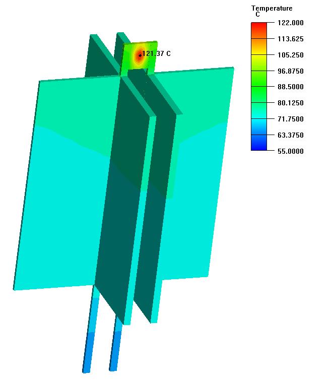
2 Agenda Gluing Soldering Sintering Transient Liquid Phase Bonding/Soldering Thermo Compression Junction Temperature Measurements
3 LED Packaging Taks Optics Filling Wire Bond 1st & 2nd Level Interconnect Chip Board Phosphor Submount Underfill Power Cooling
4 Agenda Gluing Soldering Sintering Transient Liquid Phase Bonding/Soldering Thermo Compression Junction Temperature Measurements


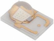
5 Glued Moduls ~ 1-2 Avago Excelitas
![R th,eff [K/W] Characterization of Thermal Interface Materials R th,int1 R th,tim Rth, eff T Q R th, eff th,int1 th, TIM th,int2 R](/docs-images/72/67340079/images/6-0.jpg "th, eff R R th,0 R 1 bulk R d A R th,int2 2,5 2,0 Linear function 1,5 1,0 TIM ~ 1/slop 0,5 R th0 0,0 0 200 400 600 800 1000 BLT")
6 R th,eff [K/W] Characterization of Thermal Interface Materials R th,int1 R th,tim Rth, eff T Q R th, eff th,int1 th, TIM th,int2 R th, eff R R th,0 R 1 bulk R d A R th,int2 2,5 2,0 Linear function 1,5 1,0 TIM ~ 1/slop 0,5 R th0 0, BLT [µm]

7 Challenges for Glued Interfaces Nanotechnologies to improve heat transfer Multi modal particles Polymer fibres & metallic alloy Surface microstructuring Nano sponge interfaces Vertically aligned CNT Nano-scale optimization TIM optimization Surface optimization Nano-scale optimization Increase thermal conductivity Increase thermal conductivity Reduce BLT Reduce interface resistance Increase thermal conductivity Improve phonon transfer


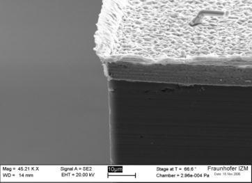
8 Failure Analyses Glued Die Bond overview focus diebond
![I [ma] Failure Analyses by Diode Characteristic 20 F9](/docs-images/72/67340079/images/9-0.jpg "15 10 A11 F1 F3 F7 F8 F9 F16 5 0 0,0 0,5 1,0 1,5 2,0 U")
9 I [ma] Failure Analyses by Diode Characteristic 20 F A11 F1 F3 F7 F8 F9 F ,0 0,5 1,0 1,5 2,0 U [V]
10 Agenda Gluing Soldering Sintering Transient Liquid Phase Bonding/Soldering Thermo Compression Junction Temperature Measurements

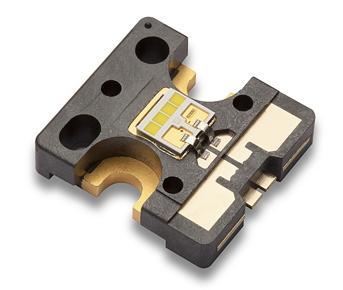
11 Soldered Moduls OSRAM


12 wire for product compatibility, but not essentiell Wireless GaN - Chips Cree DA1000 OSRAM UX:3

")
13 Wetability of LED Dice Supplier B 40 mil (LM) Supplier B 24 mil (LM)


14 Wetability of LED Dice Supplier A old design Supplier A new design


15 Wetability of LED Dice Supplier A new design Supplier A new design

16 AuSn Phase Diagram Au-rich Sn-rich 278 C e C p: +L 1 L 1 +Au 217 C e 1 ~ 60
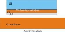
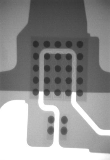
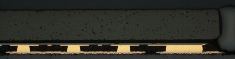
17 Copper Based LED on Silicon Substrate Reflow Soldering with AuSn no Activating Atmosphere x-ray x-ray LED-Module 1 x-ray LED-Module 2

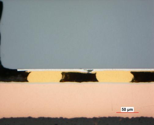
18 Copper Based LED on Silicon Substrate Reflow Soldering with AuSn no Activating Atmosphere cross section Cross Section Chip on Silicon

19 Copper Based LED on Silicon Substrate Reflow Soldering with AuSn no Activating Atmosphere cross section close up look Cross Section Chip on Silicon

20 Copper Based LED on Silicon Substrate Thermode Soldering with AuSn no Activating Atmosphere x-ray x-ray LED-Module 1 x-ray LED-Module 2
21 Copper Based LED on Silicon Substrate Thermode Soldering with AuSn no Activating Atmosphere cross section Cross Section Chip on Silicon


22 Copper Based LED on Silicon Substrate Thermode Soldering with AuSn no Activating Atmosphere cross section close up look Cross Section Chip on Silicon
23 SnAgCu Phase Diagram ~ 30


24 Copper Based LED on Silicon Substrate Reflow Soldering with SnAg with Activating Atmosphere x-ray x-ray LED-Module 1 x-ray LED-Module 2


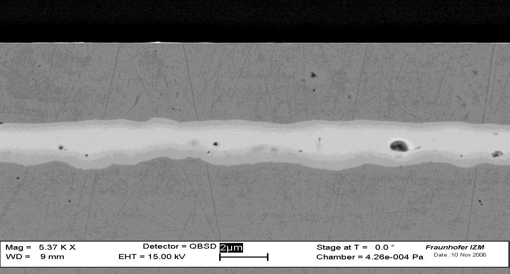
25 Copper Based LED on Silicon Substrate Reflow Soldering with SnAg with Activating Atmosphere cross section Cross Section Chip on Silicon

26 Copper Based LED on Silicon Substrate Reflow Soldering with SnAg with Activating Atmosphere cross section close up look Cross Section Chip on Silicon


27 COB assembly LEDs on AlN AlN/Si test board for optical, electrical, and thermal LED characterisation Exsample (rigth): 8 SemiLeds LEDs soldered on AlN with AuSn BMBF-Projekt Nanolux - White LEDs for General Lighting


28 Test Assembly with OSRAM LEDs OSRAM LEDs on AlN MC-PCB Subassembly mit Drahtbonds

29 OSRAM LED Dice on metallized AlN Watercooler, 600 W

30 OSRAM LED Dice on metallized AlN Watercooler, 600 W

31 OSRAM LED Dice on metallized AlN Watercooler, x-ray
32 Agenda Gluing Soldering Sintering Transient Liquid Phase Bonding/Soldering Thermo Compression Junction Temperature Measurements


33 Assembly with Ag Sintering Chip to Chip Chip to copper


34 Ag Sintering SEM Pictures Ag-Powder after drying Ag-Powder heat without force Ag-powder heat and force


35 Ag Sintered Interconnects comparing of two suppliers Cross Section with SEM preparation effect AlN Ag Plated Layer Ag Plated Layer Ag Bond Ag Bond Cu

36 Ag Sintered Interconnection, FIB Analysis Ag plated well defined interface Ag sintered

37 Ag Sintered Interconnection, FIB Analysis small pores almost disoluted ~ 370

38 OSRAM LED Dice on metallized AlN Watercooler, 1200 W


 N (8,8 ± 3,0) N (7,6 ±")
 N < 2,0 N")
39 Shear Forces for Pressure Less Sintered LEDs Temperature Chip A on Ceramic Chip B on Ceramic Chip A on IMS Chip B on IMS 225 C (8,4 ± 2,1) N (8,8 ± 3,0) N (7,6 ± 3,1) N (7,5 ± 1,5) N 275 C < 0,5 N (8,3 ± 1,9) N < 2,0 N (12,7 ± 2,9) N
40 Pressure Less Sintering pro/contra Standard Equipment (Screen printer + P&P + Reflow) No mechanical fixing of parts during sintering No special atmosphere during sintering Lower Shear forces than sintered/soldered dice Metallization of die bond pad must be suitable Smaller process windows (especially regarding drying)
41 Agenda Gluing Soldering Sintering Transient Liquid Phase Bonding/Soldering Thermo Compression Junction Temperature Measurements

42 TLPB using electroplated Cu/Sn soldering annealing Si Cu 3 Sn Cu 6 Sn 5 Cu 3 Sn Cu

 20")
 After")
43 TLPS SAC-paste plus Cu spheres Cu Cu 6 Sn 5 Sn Cu 3 Sn 40 wt.-% Cu ( Cu 6 Sn 5 ) 20 wt.-% Cu Pore 40 wt.-% Cu (Cu 6 Sn 5 ) After soldering 40 wt.-% Cu


44 TLPS SAC-paste plus 40 wt.-% Cu spheres Proprietary Process and Paste Si-Chip DAB
45 Agenda Gluing Soldering Sintering Transient Liquid Phase Bonding/Soldering Thermo Compression Junction Temperature Measurements


46 Modules Assembled by Themocompression LumiLEDs
47 Thermocompression Bonding with Stud Bumps

48 Thermocompression Bonding with electroplated Bumps
 - compressible bonding (acommodate topography) -")
 - bio compatible (e.g.")

49 Nano - Sponge Potential Application: - low pressure, low temperature bonding (MEMS, laser) - compressible bonding (acommodate topography) - containment for medical applications - large surface area (sensors, catalytics) - bio compatible (e.g. neuronal interface) 13 nm pore size - optical devices (plasmonics, SERS) Flip Chip Sintering bonding zone densified zone 80% pore volume H. Oppermann, M. Hutter, R. Jordan, et al. (Fraunhofer IZM)
50 Agenda Gluing Soldering Sintering Transient Liquid Phase Bonding/Soldering Thermo Compression Junction Temperature Measurements
51 Critical Value is the Junction Temperature T J?
52 Junction Temperature Measurement Principles 1) Wavelength shift The recombination of the electron from the conducting band (n-type semiconductor) with the holes of the valence band (p-type) is a light emitting process. As the wavelength is directly correlated to the recombination energy and therefore depending on the forward voltage, the wavelength is increasing with decreasing forward voltage and increasing temperature. 2) Forward Voltage The Forward voltage is depending on the electron band gap and the Boltzmann distribution. The Boltzmann distribution is temperature depending and therefore the voltage is decreasing with increasing temperature.
53 Concept of measuring Tj with the forward voltage I [ma] I [ma] 50 Ideal 50 II R p Real R i 0 U v U [V] 0 I U v U [V] An ideal light emitting diode is closed up to a certain voltage, the forward voltage, and afterwards open without any influence of the current. The real LED has a different behavior and can be described in an easy equivalent circuit diagram as shown above. It is influenced by resistors parallel and in serious to the junction.
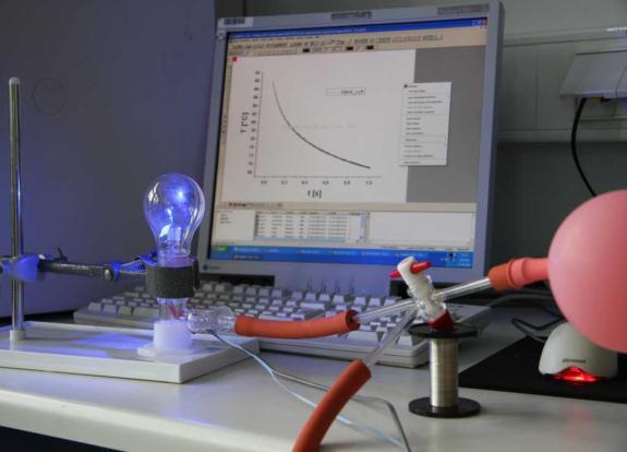
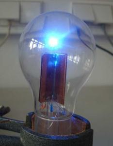
54 Strom [A] Spannung [V] Measuring Tj with the forward voltage, calibration 0,005 0,004 0,003 0,002 testing range 0,001 0,000 2,4 2,6 2,8 Spannung [V] 2,64 2,63 2,62 2,61 2,60 2,59 2,58 T = -t1 * ln (U/A1) 03B 2,637: T = -1152,913 ln(u/2,66220) 16B 2,620: T = -1398,438 ln(u/2,64008) 19B 2,640: T = -1220,828 ln(u/2,67310) 08B 2,642: T = -1179,331 ln(u/2,66607) 11B 2,634: T = -1423,025 ln(u/2,65662) 2,57 2,56 2,55 2,54 2,53 2,52 2,51 2,50 2,49 2,48 2, Temperatur [ C] The measurement current must be kept small, not to heat the die up, but out of the horizontal area of the UI characteristic, as otherwise the recalculation of the temperature will be imprecise. As Rp and Ri are different for every die, even within one lot, each LED must be calibrated.
55 Measurement Setup The internal resistance of the LED is strongly current depending and due to further distortions of higher order it is not possible to recalculate the pure forward voltage under running conditions. The running current must be lowered immediately to the measuring current, to measure the calibrated forward voltage without cooling down the LED. A possible circuit can look like the following.
56 Spannung [V] Spannung [V] Measurement Interpretation 3,2 2, mA = 2,58783 V = 25,1 C 3,0 2,56 2,8 2,55 2, T [µs] Meßpunkt [Einheit] Even within the realized switching time below 10 µs, a cooling of the LED is visible. Therefore the record transient is fitted with a biexponential curve with offset. The first half-value period is related to the thermal equilibration of the junction with the LED die, the second for the equilibration of the die with the substrate. The offset is simplified sum for the equilibration with the ambient and the final forward voltage at ambient temperature.
57 Voltage [V] Example of a Flat Panel Light Source 2,535 2,530 2,525 2,520 2,515 2,510 2,505 LED@010mA at secundary current = 010mA = 2, V = 24,16 C LED@050mA at secundary current = 050mA = 2, V = 26,44 C LED@080mA at secundary current = 080mA = 2, V = 28,51 C LED@120mA at secundary current = 120mA = 2, V = 31,72 C LED@120mA at secundary current = 080mA = 2, V = 30,08 C LED@150mA at secundary current = 150mA = 2, V = 34,28 C LED@175mA at secundary current = 175mA = 2, V = 36,11 C LED@200mA at secundary current = 200mA = 2, V = 38,66 C LED@225mA at secundary current = 225mA = 2, V = 40,91 C LED@250mA at secundary current = 250mA = 2, V = 43,52 C Time [µs]
58 Thermal comparative study gluing/soldering/sintering Test Szenario: LED auf MC-PCB, MC-PCB auf Kühlkörper, T = 25,0 C I 1 = 100 ma, I 2 = 350 ma, I 3 = 700 ma
59 U [V] Thermal comparative study gluing/soldering/sintering e.g. blue LED glued 2,44 2,42 I 1 = 100 ma 2,40 I 2 = 350 ma 2,38 I 3 = 700 ma 2,36 2,34 0,000 0,002 0,004 t [s] sample 1 sample 2 sample 3
60 T [ C] Thermal comparative study: blue LED blue glued blue soldered blue sintered thermal load (optical emission corrected) [mw]
61 T [ C] Thermal comparative study: white LED 'white' glued 'white' soldered 'white' sintered thermal load (optical emission corrected) [mw]
62 T [ C] Thermal comparative study: red LED red glued red soldered thermal load (optical emission corrected) [mw] red sintered

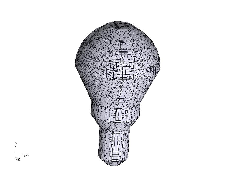
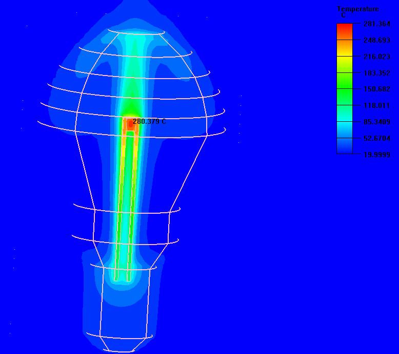
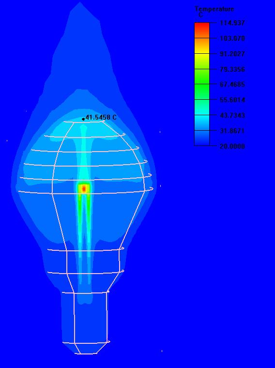
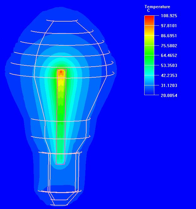
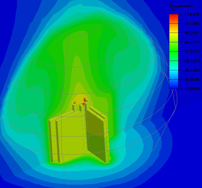
63 LED Bulb Simulation Heat sink Silicon-oil Air Helium
64 LED Bulb Simulation
Test stand for the Characterisation of Thermal Interface Materials from the macro level up to the nano level
 13th LEIBNIZ CONFERENCE OF ADVANCED SCIENCE 26. - 27. April 2012 NANOSCIENCE 2012 Test stand for the Characterisation of Thermal Interface Materials from the macro level up to the nano level Mohamad Abo
Challenges for Embedded Device Technologies for Package Level Integration
 Challenges for Embedded Device Technologies for Package Level Integration Kevin Cannon, Steve Riches Tribus-D Ltd Guangbin Dou, Andrew Holmes Imperial College London Embedded Die Technology IMAPS-UK/NMI
Fraunhofer IZM Bump Bonding and Electronic Packaging
 Fraunhofer IZM Bump Bonding and Electronic Packaging Fraunhofer Institute for Reliability and Microintegration (IZM) Gustav-Meyer-Allee 25 13355 Berlin Germany Dipl.-Ing. Thomas Fritzsch Contact: thomas.fritzsch@izm.fraunhofer.de
TIMAwave a novel test stand for thermal diffusivity measurement based on the Angstrom s method
 1 TIMAwave a novel test stand for thermal diffusivity measurement based on the Angstrom s method 12th European Advanced Technology Workshop on Micropackaging and Thermal management La Rochelle, France
Universal Test System for the Characterization of the most common Thermal Interface Materials
 7 th European Advanced Technology Workshop on Micropackaging and Thermal Management La Rochelle, February 1 st, 2012 Universal Test System for the Characterization of the most common Thermal Interface
Development of an Low Cost Wafer Level Flip Chip Assembly Process for High Brightness LEDs Using the AuSn Metallurgy
 Development of an Low Cost Wafer Level Flip Chip Assembly Process for High Brightness LEDs Using the AuSn Metallurgy Gordon Elger, Rafael Jordan, Maria v. Suchodoletz and Hermann Oppermann Fraunhofer Institute
LED Die Attach Selection Considerations
 LED Die Attach Selection Considerations Gyan Dutt & Ravi Bhatkal Alpha, An Alent plc Company Abstract Die attach material plays a key role in performance and reliability of mid, high and super-high power
Study and mechanical characterization of high temperature power electronic packaging
 Study and mechanical characterization of high temperature power electronic packaging A. BAAZAOUI a, O. DALVERNY a, J. ALEXIS a, M. KARAMA a a. Université de Toulouse; INP/ENIT; LGP ; 47 avenue d'azereix;
CERN/NA62 GigaTracKer Hybrid Module Manufacturing
 CERN/NA62 GigaTracKer Hybrid Module Manufacturing Fraunhofer Institute for Reliability and Microintegration Gustav-Meyer-Allee 25 13355 Berlin Germany Dipl.-Ing. Thomas Fritzsch Contact: Fraunhofer IZM
9 rue Alfred Kastler - BP Nantes Cedex 3 - France Phone : +33 (0) website :
 website :") 9 rue Alfred Kastler - BP 10748-44307 Nantes Cedex 3 - France Phone : +33 (0) 240 180 916 - email : info@systemplus.fr - website : www.systemplus.fr November 2010 - Version 2 Written by: Sylvain HALLEREAU
9 rue Alfred Kastler - BP 10748-44307 Nantes Cedex 3 - France Phone : +33 (0) 240 180 916 - email : info@systemplus.fr - website : www.systemplus.fr November 2010 - Version 2 Written by: Sylvain HALLEREAU
Novel Technique for Flip Chip Packaging of High power Si, SiC and GaN Devices. Nahum Rapoport, Remtec, Inc.
 Novel Technique for Flip Chip Packaging of High power Si, SiC and GaN Devices Nahum Rapoport, Remtec, Inc. 1 Background Electronic Products Designers: under pressure to decrease cost and size Semiconductor
3D Wirebondless IGBT Module for High Power Applications Dr. Ziyang GAO Jun. 20, 2014
 3D Wirebondless IGBT Module for High Power Applications Dr. Ziyang GAO Jun. 20, 2014 1 1 Outline Background Information Technology Development Trend Technical Challenges ASTRI s Solutions Concluding Remarks
Comparison of OSRAM OSTAR Headlamp Pro and OSLON Black Flat Application Note
 Comparison of OSRAM OSTAR Headlamp Pro and Application Note Abstract In this application note a new SMD LED type is presented as an alternative to existing LEDs to create multi-chip light sources for diverse
9 rue Alfred Kastler - BP Nantes Cedex 3 - France Phone : +33 (0) website :
 website :") 9 rue Alfred Kastler - BP 10748-44307 Nantes Cedex 3 - France Phone : +33 (0) 240 180 916 - email : info@systemplus.fr - website : www.systemplus.fr November 2010 - Version 2 Written by: Sylvain HALLEREAU
9 rue Alfred Kastler - BP 10748-44307 Nantes Cedex 3 - France Phone : +33 (0) 240 180 916 - email : info@systemplus.fr - website : www.systemplus.fr November 2010 - Version 2 Written by: Sylvain HALLEREAU
YOUR Strategic TESTING ENGINEERING CONCEPT SMT FLIP CHIP PRODUCTION OPTO PACKAGING PROCESS DEVELOPMENT CHIP ON BOARD SUPPLY CHAIN MANAGEMENT
 YOUR Strategic TECHNOLOGY PARTNER Wafer Back-End OPTO PACKAGING PROCESS DEVELOPMENT CONCEPT FLIP CHIP PROTOTYping ENGINEERING TESTING SMT PRODUCTION CHIP ON BOARD SUPPLY CHAIN MANAGEMENT Next Level 0f
Adaption to scientific and technical progress under Directive 2002/95/EC
 . Adaption to scientific and technical progress under Directive 2002/95/EC Results previous evaluation Exemption No. 15 Lead in solders to complete a viable electrical connection between semiconductor
Adaption to scientific and technical progress under Directive 2002/95/EC
 . Adaption to scientific and technical progress under Directive 2002/95/EC Results previous evaluation Exemption No. 7 a a) Lead in high melting temperature type solders (i.e. lead-based alloys containing
A New Thermal Management Material for HBLEDs based on Aluminum Nitride Ceramics
 A New Thermal Management Material for HBLEDs based on Aluminum Nitride Ceramics Thermal Management Challenges in HBLED Excess heat leads to a whole range of performance and reliability issues for high
Fixed Resistors INSULATED ALUMINUM SUBSTRATES. Thermal Solutions for Hi Brightness LED Applications - Application Note
 INSULATED ALUMINUM SUBSTRATES TT electronics is a leading designer and manufacturer of electronic components. As a result of our experience with power components, Anotherm substrates were developed as
YOUR Strategic TESTING ENGINEERING CONCEPT SMT FLIP CHIP PRODUCTION OPTO PACKAGING PROCESS DEVELOPMENT CHIP ON BOARD SUPPLY CHAIN MANAGEMENT
 YOUR Strategic TECHNOLOGY PARTNER Wafer Back-End OPTO PACKAGING PROCESS DEVELOPMENT CONCEPT FLIP CHIP PROTOTYping ENGINEERING TESTING SMT PRODUCTION CHIP ON BOARD SUPPLY CHAIN MANAGEMENT Next Level 0f
5. Packaging Technologies Trends
 5. Packaging Technologies Trends Electronic products and microsystems continue to find new applications in personal, healthcare, home, automotive, environmental and security systems. Advancements in packaging
 Law, T.K., Lim, F., Li, Y., Teo, J.W. R. and Wei, S. (2017) Effects of Humidity on the Electro-Optical-Thermal Characteristics of High-Power LEDs. In: 2016 IEEE 18th Electronics Packaging Technology Conference
CO.,LTD.,314,Maetan3-Dong,Yeongtong-Gu,Suwon,Gyunggi-Do,Korea,
 Key Engineering Materials Vols. 326-328 (2006) pp 309-32 Online: 2006-2-0 (2006) Trans Tech Publications, Switzerland doi:0.4028/www.scientific.net/kem.326-328.309 MEMS based metal plated silicon package
FRAUNHOFER INSTITUTE FOR RELIABILITY AND MICROINTEGRATION IZM DEPARTMENT WAFER LEVEL SYSTEM INTEGRATION BERLIN
 FRAUNHOFER INSTITUTE FOR RELIABILITY AND MICROINTEGRATION IZM DEPARTMENT WAFER LEVEL SYSTEM INTEGRATION BERLIN WAFER LEVEL SYSTEM INTEGRATION ELECTRONIC PACKAGING AT FRAUNHOFER IZM The Fraunhofer Institute
Power Electronics Packaging Solutions for Device Junction Temperature over 220 o C
 EPRC 12 Project Proposal Power Electronics Packaging Solutions for Device Junction Temperature over 220 o C 15 th August 2012 Page 1 Motivation Increased requirements of high power semiconductor device
FRAUNHOFER INSTITUTE FOR RELIABILITY AND MICROINTEGRATION IZM DEPARTMENT WAFER LEVEL SYSTEM INTEGRATION BERLIN
 FRAUNHOFER INSTITUTE FOR RELIABILITY AND MICROINTEGRATION IZM DEPARTMENT WAFER LEVEL SYSTEM INTEGRATION BERLIN WAFER LEVEL SYSTEM INTEGRATION ELECTRONIC PACKAGING AT FRAUNHOFER IZM The Fraunhofer Institute
High Efficiency UV LEDs Enabled by Next Generation Substrates. Whitepaper
 High Efficiency UV LEDs Enabled by Next Generation Substrates Whitepaper Introduction A primary industrial market for high power ultra-violet (UV) LED modules is curing equipment used for drying paints,
PCTB PC-LAB. Power Cycling Testbench for Power Electronic Modules. Power Cycling Test Laboratory
 PCTB Power Cycling Testbench for Power Electronic Modules PC-LAB Power Cycling Test Laboratory Technical Information PCTB power cycling test bench alpitronic has many years of experience in developing
Effect of Multiple Flip-Chip Assembly on Joint Strength of AuSn solder in Hybrid Compact Optoelectronic Module
 1 Effect of Multiple Flip-Chip Assembly on Joint Strength of AuSn solder in Hybrid Compact Optoelectronic Module K.-M. Chu, Student Member, IEEE, J.-S. Lee, H. Oppermann, G. Engelmann, J. Wolf, H. Reichl,
FLIP-CHIP TECHNOLOGIES AND GLOBAL MARKETS
 FLIP-CHIP TECHNOLOGIES AND GLOBAL MARKETS SMC089B July 2016 Sinha G. Project Analyst ISBN: 1-62296-329-6 BCC Research 49 Walnut Park, Building 2 Wellesley, MA 02481 USA 866-285-7215 (toll-free within the
Processor Performance, Packaging and Reliability Utilizing a Phase Change Metallic Alloy Thermal Interface System
 Processor Performance, Packaging and Reliability Utilizing a Phase Change Metallic Alloy Thermal Interface System Chris G. Macris, Thomas R. Sanderson, Robert G. Ebel, Christopher B. Leyerle Enerdyne Solutions,
Chapter 3 Silicon Device Fabrication Technology
 Chapter 3 Silicon Device Fabrication Technology Over 10 15 transistors (or 100,000 for every person in the world) are manufactured every year. VLSI (Very Large Scale Integration) ULSI (Ultra Large Scale
Advanced Power Modules with AlN-Substrates Extending Current Capability and Lifetime
 Advanced Power Modules with AlN-Substrates Extending Current Capability and Lifetime U.Scheuermann SEMIKRON Elektronik GmbH, Sigmundstraße 2, 9431 Nuremberg, Germany Tel.: ++49-911-6559-381 Fax: ++49-911-6559-414
Fraunhofer ENAS Current results and future approaches in Wafer-level-packaging FRANK ROSCHER
 Fraunhofer ENAS - Current results and future approaches in Wafer-level-packaging FRANK ROSCHER Fraunhofer ENAS Chemnitz System Packaging Page 1 System Packaging Outline: Wafer level packaging for MEMS
Wafer-to-Wafer Bonding and Packaging
 Wafer-to-Wafer Bonding and Packaging Dr. Thara Srinivasan Lecture 25 Picture credit: Radant MEMS Reading Lecture Outline Senturia, S., Chapter 17, Packaging. Schmidt, M. A. Wafer-to-Wafer Bonding for Microstructure
Fraunhofer IZM. All Silicon System Integration Dresden Scope. M. Juergen Wolf
 Fraunhofer IZM All Silicon System Integration Dresden Scope M. Juergen Wolf Fraunhofer IZM All Silicon System Integration - ASSID Dresden, Berlin, Germany Fraunhofer IZM Focus of Activities Materials,
Power Electronics Packaging Revolution Module without bond wires, solder and thermal paste
 SEMIKRON Pty Ltd 8/8 Garden Rd Clayton Melbourne 3168 VIC Australia Power Electronics Packaging Revolution Module without bond wires, solder and thermal paste For some years now, the elimination of bond
Preliminary Ultraviolet Emitter
 Preliminary Ultraviolet Emitter Product No: MTSM395UV-FP7140 Peak Emission Wavelength: 395 nm The MTSM395UV-FP7140 is a ultraviolet light emitting diode with peak emission wavelength of 395nm. The High
High-Temperature-Resistant Interconnections Formed by Using Nickel Micro-plating and Ni Nano-particles for Power Devices
 Kato et al.: High-Temperature-Resistant Interconnections (1/6) [Technical Paper] High-Temperature-Resistant Interconnections Formed by Using Nickel Micro-plating and Ni Nano-particles for Power Devices
Chapter 4 Fabrication Process of Silicon Carrier and. Gold-Gold Thermocompression Bonding
 Chapter 4 Fabrication Process of Silicon Carrier and Gold-Gold Thermocompression Bonding 4.1 Introduction As mentioned in chapter 2, the MEMs carrier is designed to integrate the micro-machined inductor
Building HDI Structures using Thin Films and Low Temperature Sintering Paste
 Building HDI Structures using Thin Films and Low Temperature Sintering Paste Catherine Shearer, James Haley and Chris Hunrath Ormet Circuits Inc. - Integral Technology California, USA chunrath@integral-hdi.com
A Novel Thermal Management Approach for Packaging of High Power GaN Devices
 A Novel Thermal Management Approach for Packaging of High Power GaN Devices April 6 th, 2016 1 000304 Agenda - Thermal Management Flange and Package Materials - GaN High Power Densities and the New RF
FLIP CHIP CHIP ON BOARD SMT ENGINEERING OPTO PACKAGING SUPPLY CHAIN MANAGEMENT TESTING YOUR INNOVATIVE TECHNOLOGY PARTNER PRODUCTION CONCEPT
 YOUR INNOVATIVE TECHNOLOGY PARTNER CHIP ON BOARD OPTO PACKAGING PROCESS DEVELOPMENT CONCEPT FLIP CHIP ENGINEERING TESTING PRODUCTION SMT SUPPLY CHAIN MANAGEMENT PROTOTYPES HIGH-PRECISION ASSEMBLY OF MICRO-
3D technologies for integration of MEMS
 3D technologies for integration of MEMS, Fraunhofer Institute for Electronic Nano Systems Folie 1 Outlook Introduction 3D Processes Process integration Characterization Sample Applications Conclusion Folie
Lead-Free Solder Bump Technologies for Flip-Chip Packaging Applications
 Lead-Free Solder Bump Technologies for Flip-Chip Packaging Applications Zaheed S. Karim 1 and Jim Martin 2 1 Advanced Interconnect Technology Ltd. 1901 Sunley Centre, 9 Wing Yin Street, Tsuen Wan, Hong
TSV Processing and Wafer Stacking. Kathy Cook and Maggie Zoberbier, 3D Business Development
 TSV Processing and Wafer Stacking Kathy Cook and Maggie Zoberbier, 3D Business Development Outline Why 3D Integration? TSV Process Variations Lithography Process Results Stacking Technology Wafer Bonding
Dynamic and Cooler. Duet F200. Best Lumen / Watt Plant Growth COB Module
 Best Lumen / Watt Plant Growth COB Module Dynamic and Cooler High Efficacy & Lower Thermal Resistance Duet F200 is a 200W COB series offering 5 different PPFD ratios between 450nm Blue and Broadband 600nm700nm
CX Thin Fil s. Resistors Attenuators Thin-Film Products Thin-Film Services. ISO 9001:2008 RoHS/REACH Compliant ITAR Compliant
 CX Thin Fil s Resistors Attenuators Thin-Film Products Thin-Film Services www.cxthinfilms.com ISO 9001:2008 RoHS/REACH Compliant ITAR Compliant www.cxthinfilms.com sales@cxthinfilms.com +1 (401) 461-5500
Grundlagen der LED Technik
 www.osram-os.com Grundlagen der LED Technik Dr. Berthold Hahn 8.3.14 Ilmenau 1 Dateienname ORG CODE Initiale Titel/Veranstaltung TT/MM/JJJJ Grundlagen der LED Technik 1. Einführung 2. Lichterzeugung im
ALTERNATIVES TO SOLDER IN INTERCONNECT, PACKAGING, AND ASSEMBLY
 ALTERNATIVES TO SOLDER IN INTERCONNECT, PACKAGING, AND ASSEMBLY Herbert J. Neuhaus, Ph.D., and Charles E. Bauer, Ph.D. TechLead Corporation Portland, OR, USA herb.neuhaus@techleadcorp.com ABSTRACT Solder
Composition/wt% Bal SA2 (SABI) Bal SA3 (SABI + Cu) Bal
 Bal SA3 (SABI + Cu) Bal") Improving Thermal Cycle and Mechanical Drop Impact Resistance of a Lead-free Tin-Silver-Bismuth-Indium Solder Alloy with Minor Doping of Copper Additive Takehiro Wada 1, Seiji Tsuchiya 1, Shantanu Joshi
Improving Thermal Cycle and Mechanical Drop Impact Resistance of a Lead-free Tin-Silver-Bismuth-Indium Solder Alloy with Minor Doping of Copper Additive Takehiro Wada 1, Seiji Tsuchiya 1, Shantanu Joshi
Materials for LED packaging
 www.osram-os.com Materials for LED packaging Dr. N. von Malm June 2018 Chemnitz Agenda 1. Introduction: Materials for LEDs 2. Packaging Materials 3. Materials for color conversion (Phosphors) 2 Advanced
Developments in low-temperature metal-based packaging
 Developments in low-temperature metal-based packaging 2011. 12.14 Jiyoung Chang and Liwei Lin Ph.D. Candidate, Department of Mechanical Engineering University of California at Berkeley 1 1 Contents Project
Packaging Technologies for SiC Power Modules
 Packaging Technologies for SiC Power Modules Masafumi Horio Yuji Iizuka Yoshinari Ikeda ABSTRACT Wide bandgap materials such as silicon carbide (SiC) and gallium nitride (GaN) are attracting attention
PROCESSING AND RELIABILITY OF LOW-SILVER-ALLOYS
 PROCESSING AND RELIABILITY OF LOW-SILVER-ALLOYS Mathias Nowottnick and Andrej Novikov University of Rostock Rostock, Germany mathias.nowottnick@uni-rostock.de Joerg Trodler W.C. Heraeus Hanau, Germany
SLID bonding for thermal interfaces. Thermal performance. Technology for a better society
 SLID bonding for thermal interfaces Thermal performance Outline Background and motivation The HTPEP project Solid-Liquid Inter-Diffusion (SLID) Au-Sn SLID Cu-Sn SLID Reliability and bond integrity Alternative
Research Article Thermal Characteristics of InGaN/GaN Flip-Chip Light Emitting Diodes with Diamond-Like Carbon Heat-Spreading Layers
 International Photoenergy, Article ID 829284, 5 pages http://dx.doi.org/1.1155/214/829284 Research Article Thermal Characteristics of InGaN/GaN Flip-Chip Light Emitting Diodes with Diamond-Like Carbon
Bonding Technologies for 3D-Packaging
 Dresden University of Technology / Karsten Meier, Klaus-Juergen Wolter NanoZEIT seminar @ SEMICON Europa 2011 Dresden System integration by SoC or SiP solutions offer advantages regarding design efforts,
Future Electronic Devices Technology in Cosmic Space and Lead-free Solder Joint Reliability
 The 22nd Microelectronics Work Future Electronic Devices Technology in Cosmic Space and Lead-free Solder Joint Reliability Key Points (1) High Speed Solder Ball Shear Test (2) Relationship between Surface
Advanced Analytical Techniques for Semiconductor Assembly Materials and Processes. Jason Chou and Sze Pei Lim Indium Corporation
 Advanced Analytical Techniques for Semiconductor Assembly Materials and Processes Jason Chou and Sze Pei Lim Indium Corporation Agenda Company introduction Semiconductor assembly roadmap challenges Fine
Innovative MID Plating Solutions
 Innovative MID Plating Solutions High Reliability Wire Bond Technique for MIDs Jordan Kologe MacDermid Electronics Solutions jkologe@macdermid.com 1 MacDermid: Specialty Chemical Solutions Over 2000 Worldwide
Application Note AN 992
 Beam Lead Attachment Methods Application Note AN 992 Description This application note gives the first time user a general description of various attachment methods for beam lead devices. The attached
Cree EZ1950-p LEDs Data Sheet (Anode up) CxxxEZ1950-Sxxxx00-x
 CxxxEZ1950-Sxxxx00-x") Cree EZ195-p LEDs Data Sheet (Anode up) CxxxEZ195-Sxxxx-x Cree s EZBright LEDs are the newest generation of solid-state LED emitters that combine highly efficient InGaN materials with Cree s proprietary
Cree EZ195-p LEDs Data Sheet (Anode up) CxxxEZ195-Sxxxx-x Cree s EZBright LEDs are the newest generation of solid-state LED emitters that combine highly efficient InGaN materials with Cree s proprietary
Thermal Analysis of High Power Pulse Laser Module
 Thermal Analysis of High Power Pulse Laser Module JinHan Ju PerkinElmer Optoelectronics Salem MA 01970 Abstract Thermal management is very critical in laser diode packaging, especially for a high power
Advanced Power Module Packaging for increased Operation Temperature and Power Density
 15th International Power Electronics and Motion Control Conference, EPE-PEMC 2012 ECCE Europe, Novi Sad, Serbia Advanced Power Module Packaging for increased Operation Temperature and Power Density Peter
Maximum MAX662 12V DC-DC Converter
 Construction Analysis Maximum MAX662 12V DC-DC Converter Report Number: SCA 9512-445 Global Semiconductor Industry the Serving Since 1964 17350 N. Hartford Drive Scottsdale, AZ 85255 Phone: 602-515-9780
2W, 2512, 4-Terminal, Low Resistance Chip Resistor (Lead / Halogen Free)
") 2W, 2512, 4-Terminal, Low Resistance Chip Resistor (Lead / Halogen Free) 1. Scope This specification applies to 3.2mm x 6.4mm size 2W, fixed metal foil with ceramic carrier current sensing resistors used
2W, 2512, 4-Terminal, Low Resistance Chip Resistor (Lead / Halogen Free) 1. Scope This specification applies to 3.2mm x 6.4mm size 2W, fixed metal foil with ceramic carrier current sensing resistors used
Flexible Substrates for Smart Sensor Applications
 Flexible Substrates for Smart Sensor Applications A novel approach that delivers miniaturized, hermetic, biostable and highly reliable smart sensor modules. AUTHORS Dr. Eckardt Bihler, Dr. Marc Hauer,
Reliability of RoHS-Compliant 2D and 3D 1С Interconnects
 Reliability of RoHS-Compliant 2D and 3D 1С Interconnects John H. Lau, Ph.D. New York Chicago San Francisco Lisbon London Madrid Mexico City Milan New Delhi San Juan Seoul Singapore Sydney Toronto Foreword
EV Group 300mm Wafer Bonding Technology July 16, 2008
 EV Group 300mm Wafer Bonding Technology July 16, 2008 EV Group in a Nutshell st Our philosophy Our mission in serving next generation application in semiconductor technology Equipment supplier for the
PCB Technologies for LED Applications Application note
 PCB Technologies for LED Applications Application note Abstract This application note provides a general survey of the various available Printed Circuit Board (PCB) technologies for use in LED applications.
1.3.2 Nanotechnology Nanoporosity Deposition Methods Dissolution Methods
 Table of Contents 1. Metal Finishing 1 1.1 Introduction 1 1.1.1 Description of Industrial Activity Covered 1 1.1.2 Environmental and Legislative Background 3 1.1.3 Emerging Technology or Research? 4 1.2
Multiple-Layer Heat Dissipation Module for LED Streetlamps
 Journal of Applied Science and Engineering, Vol. 15, No. 2, pp. 97 104 (2012) 97 Multiple-Layer Heat Dissipation Module for LED Streetlamps Shung-Wen Kang*, Kun-Cheng Chien and Wei-Chung Lin Department
MEPTEC Semiconductor Packaging Technology Symposium
 MEPTEC Semiconductor Packaging Technology Symposium Advanced Packaging s Interconnect Technology Process Shift and Direction October 23, 2014 Jay Hayes- Director of Business Development -Bumping and Flip
Semiconductor Nanostructures
 II H. von Känel Laboratorium für Festkörperphysik ETHZ Applications Lighting Field effect transistors Sensors Infrared sensors X-ray detectors Periodic table of elements Comparison of wurtzite and zinc-
Development of a Fluxless Flip Chip Bonding Process for Optical Military Electronics
 Development of a Fluxless Flip Chip Bonding Process for Optical Military Electronics Michael Girardi, Daric Laughlin, Philip Abel, Steve Goldammer, John Smoot NNSA s Kansas City Plant managed by Honeywell
Electrical and Fluidic Microbumps and Interconnects for 3D-IC and Silicon Interposer
 Electrical and Fluidic Microbumps and Interconnects for 3D-IC and Silicon Interposer Li Zheng, Student Member, IEEE, and Muhannad S. Bakir, Senior Member, IEEE Georgia Institute of Technology Atlanta,
LED Packaging Innovations for Smart Lighting Systems
 Outline LED Packaging Innovations for Smart Lighting Systems James J.-Q. Lu Rensselaer Polytechnic Institute (RPI), Troy, NY, USA Introduction to Smart Lighting LED Packaging Challenges Advances in LED
3D Stacking of Chips with Electrical and Microfluidic I/O Interconnects
 3D Stacking of Chips with Electrical and Microfluidic I/O Interconnects Calvin R. King, Jr., Deepak Sekar, Muhannad S. Bakir, Bing Dang #, Joel Pikarsky, and James D. Meindl Georgia Institute of Technology,
Ultra Fine Pitch Bumping Using e-ni/au and Sn Lift-Off Processes
 Ultra Fine Pitch Bumping Using e-ni/au and Sn Lift-Off Processes Andrew Strandjord, Thorsten Teutsch, and Jing Li Pac Tech USA Packaging Technologies, Inc. Santa Clara, CA USA 95050 Thomas Oppert, and
Double-side cooled semiconductors for automotive applications
 Double-side cooled semiconductors for automotive applications Dr. Martin Schneider-Ramelow, Fraunhofer IZM Berlin, D Thomas Baumann, Fraunhofer IZM Berlin, D Dr. Eckart Hoene, Fraunhofer IZM Berlin, D
Heat Transfer Characteristics in High Power LED Packaging
 Heat Transfer Characteristics in High Power LED Packaging Chi-Hung Chung 1, Kai-Shing Yang 2,*, Kuo-Hsiang Chien 2, Ming-Shan Jeng 2 and Ming-Tsang Lee 1, 1 Department of Mechanical Engineering, National
FYS4260/FYS9260: Microsystems and Electronics Packaging and Interconnect. Metallization and Interconnects
 FYS4260/FYS9260: Microsystems and Electronics Packaging and Interconnect Metallization and Interconnects Learning objectives Metal heros Significance of selecting right metallization systems and examples
Mosel Vitelic MS62256CLL-70PC 256Kbit SRAM
 Construction Analysis Mosel Vitelic MS62256CLL-70PC 256Kbit SRAM Report Number: SCA 9703-499 Global Semiconductor Industry the Serving Since 1964 17350 N. Hartford Drive Scottsdale, AZ 85255 Phone: 602-515-9780
Bridging Supply Chain Gap for Exempt High-Reliability OEM s
 Bridging Supply Chain Gap for Exempt High-Reliability OEM s Hal Rotchadl hrotchadl@premiers2.com www.premiers2.com Premier Semiconductor Services Tempe, AZ RoHS exempt high reliability OEMs breathed a
Welcome Packaging Research in Electronic Energy Systems (PREES) CIRCUIT DESIGN BEYOND THE SCHEMATIC
 CIRCUIT DESIGN BEYOND THE SCHEMATIC") Characterization of Ultra-Thin Flexible Ceramics for High-Density, 3D-Stackable Substrates for Wearable Power Electronics Xin Zhao Bo Gao Douglas C. Hopkins North Carolina State University Presented at
Characterization of Ultra-Thin Flexible Ceramics for High-Density, 3D-Stackable Substrates for Wearable Power Electronics Xin Zhao Bo Gao Douglas C. Hopkins North Carolina State University Presented at
1 Thin-film applications to microelectronic technology
 1 Thin-film applications to microelectronic technology 1.1 Introduction Layered thin-film structures are used in microelectronic, opto-electronic, flat panel display, and electronic packaging technologies.
ECE414/514 Electronics Packaging Spring 2012 Lecture 2. Lecture Objectives
 ECE414/514 Electronics Packaging Lecture 2 James E. Morris Dept of Electrical & Computer Engineering Portland State University Lecture Objectives Introduce first-level interconnect technologies: wire-bond,
Dark current measurements of diodes on two SLID test wafers
 Dark current measurements of diodes on two SLID test wafers Information collected by M. Beimforde for the MPP Inner Detector Upgrade Working Group August 16, 2007 Abstract In this short report the dark
EP A2 (19) (11) EP A2 (12) EUROPEAN PATENT APPLICATION. (43) Date of publication: Bulletin 2006/23
 (11) EP A2 (12) EUROPEAN PATENT APPLICATION. (43) Date of publication: Bulletin 2006/23") (19) Europäisches Patentamt European Patent Office Office européen des brevets (12) EUROPEAN PATENT APPLICATION (11) EP 1 667 226 A2 (43) Date of publication: 07.06.06 Bulletin 06/23 (1) Int Cl.: H01L
(19) Europäisches Patentamt European Patent Office Office européen des brevets (12) EUROPEAN PATENT APPLICATION (11) EP 1 667 226 A2 (43) Date of publication: 07.06.06 Bulletin 06/23 (1) Int Cl.: H01L
3D-IC Integration using D2C or D2W Alignment Schemes together with Local Oxide Reduction
 3D-IC Integration using D2C or D2W Alignment Schemes together with Local Oxide Reduction Gilbert Lecarpentier*, Jean-Stéphane Mottet* SET S.A.S. (Smart Equipment Technology), 131 Impasse Barteudet, 74490
Revised RoHS Annex As of 1 st January Entered force 24 September 2010, corrected 29 September 2010*
 Revised RoHS Annex As of 1 st January 2011. Entered force 24 September 2010, corrected 29 September 2010* 1 1 Mercury in single capped (compact) fluorescent lamps not exceeding (per burner): 1(a) For general
5W White SPHWHTA3N500
 Product Family Data Sheet Rev. 00 2016.11.01 111 High Power LED Ceramic Series 5W White SPHWHTA3N500 Features & Benefits Package : Silicone covered ceramic substrate Dimension : 3.5 mm x 3.5 mm Technology
II. A. Basic Concept of Package.
 Wafer Level Package for Image Sensor Module Won Kyu Jeung, Chang Hyun Lim, Jingli Yuan, Seung Wook Park Samsung Electro-Mechanics Co., LTD 314, Maetan3-Dong, Yeongtong-Gu, Suwon, Gyunggi-Do, Korea 440-743
Study of High Power COB LED Modules with Respect to Topology of Chips
 Study of High Power COB LED Modules with Respect to Topology of Chips Nikolay Vakrilov 1), Anna Andonova 1), and Nadejda Kafadarova 2) 1) FEET, Technical University of Sofia, Sofia, Bulgaria 2) Faculty
JOINT INDUSTRY STANDARD
 JOINT INDUSTRY STANDARD AUGUST 1999 Semiconductor Design Standard for Flip Chip Applications ASSOCIATION CONNECTING ELECTRONICS INDUSTRIES Semiconductor Design Standard for Flip Chip Applications About
Nano- And Micro-Filled Conducting Adhesives For Z-axis Interconnects
 Nano- And Micro-Filled Conducting Adhesives For Z-axis Interconnects We take a look at micro-filled epoxy-based conducting adhesives modified with nanoparticles for z- axis interconnections, especially
Materials Characterization for Stress Management
 Materials Characterization for Stress Management Ehrenfried Zschech, Fraunhofer IZFP Dresden, Germany Workshop on Stress Management for 3D ICs using TSVs San Francisco/CA, July 13, 2010 Outline Stress
Manufacturing and Reliability Modelling
 Manufacturing and Reliability Modelling Silicon Chip C Bailey University of Greenwich London, England Printed Circuit Board Airflow Temperature Stress at end of Reflow Stress Product Performance in-service
Advancements In Packaging Technology Driven By Global Market Return. M. G. Todd
 Advancements In Packaging Technology Driven By Global Market Return M. G. Todd Electronic Materials, Henkel Corporation, Irvine, California 92618, USA Recently, the focus of attention in the IC packaging