Fysisk institutt, Universitetet i Oslo Lille Fysiske Auditorium 10. and 17. Mars John Steinar Johnsen Senior Application Engineer PCB
|
|
|
- Candice Banks
- 6 years ago
- Views:
Transcription
1 Fysisk institutt, Universitetet i Oslo Lille Fysiske Auditorium 10. and 17. Mars 2014 John Steinar Johnsen Senior Application Engineer PCB -Printed Circuit Board-
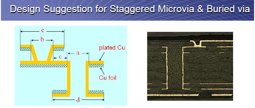
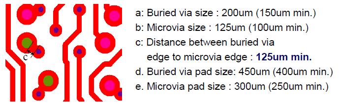
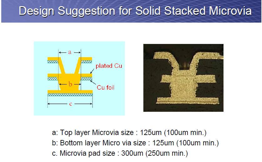
2 Program for 10. and 17. Mars 2014 Time, 12:15 14:00 both days. - Mini BoardWalk, Schematic Simplified Tour of the PCB Manufacturing Processes - A view on different PCB build up s, EMC considerations, PWR, GND and signals. - Build in capasitance (BC Core), de-coupling - Some stuff on PCB Materials, copper structure, glass and epoxy. Specify according to IPC 4101C/xxx - Advanced HDI PCBs, microvia holes, buried vias, stacked and staggered microvia holes, buried holes. - Design Rules, design aspects, errors seen. - Introduction to Flexible and FlexRigid PCBs - Introduction to MBPCB Metal Back PCB s. Aluminium for Power and LED applications.
3 A view on different PCB build up s, EMC considerations, PWR, GND and signals
4 DESIGN RULES Layer stack-up (Balanced build): In order to review for the balanced build, consider an imaginary line in the middle of the board. This will divide the board into upper and lower half. The copper layers in the top half of the board should match with the bottom half of the circuit board. The layer to layer spacing in the top half of the board should match with the bottom half of the board. The material used in the upper and lower half of the board should be the same to avoid warpage. The stack-up for hybrid circuits should be reviewed by design to design basis.

5 4 layer Standard 1.6mm foil build It is common to see four layer boards stacked as above. 2 layer core with 2 foil layers. That is, four evenly spaced layers with the planes in the centre. Although, this certainly makes the board symmetrical it doesn t help the EMC. To put the power planes closer in the middle certainly creates good inter plane capacitance, but it doesn t help with signal integrity, crosstalk or EMC

6 6 layer Standard 1.6mm foil build A six layer board is basically a four layer board with two extra signal layers added between the planes. This improves the EMI dramatically as it provides two buried layers for high-speed signals and two surface layers for routing low speed signals.

7 8 layer Standard 1.6mm foil build To improve EMC performance, add two more planes to the six layer stackup. In the case below, two plane layers are added to the centre of the substrate. This allows tight coupling between the centre planes and isolates each signal plane reducing coupling hence crosstalk dramatically. This configuration is commonly used for high speed signals of DDR2 and DDR3 designs where crosstalk due to tight routing is an issue.

8 10 layer Standard 1.6mm foil build A ten layer board should be used when six routing layers and four planes are required and EMC is of concern. This stackup is ideal because of the tight coupling of the signal and return planes, the shielding of the high speed signal layers, the existence of multiple ground planes, as well as a tightly coupled power/ground plane. Prepared for mvia use

9 12 layer Standard 1.6mm foil build The above twelve layer, 2 signal layers are added in the middle, and stackup provides shielding on six of the internal layers. Prepared for mvia use

10 The fourteen layer stackup below is used when eight routing (signal) layers are required plus special shield of critical nets is required. Layers 6 and 9 provide isolation for sensitive signals while layers 3 & 4 and 11 & 12 provide shielding for high speed signals. 14 layer Standard 1.8mm foil build Prepared for mvia use

11 A sixteen layer PCB provides ten layers of routing and is normally used for very dense designs. Repeated arguments from layer sstackups. 16 layer Standard 1.8mm foil build


 16 layer 1.")
12 A sixteen layer 1.6mm based on only 3 cores. This build is adapted for 5 microvias stacked or staggered. ( 1-2 / 2-3 / 3-4 / 4-5 / 5-6 ) and indentical ( ) 16 layer 1.6mm foil build, microvia via
13
14 - Build in capasitance - (BC Core), de-coupling
15 Buried Capacitance --BC-- Product Family will improve your - Power Distribution System (PDS) - Noise margin and improve - EMC levels.
16 A Very Simple Idea Use the Power and Ground Planes to Form Buried Capacitance (BC) Planes Within the PCB, and Remove Most of the Bypass Capacitors Remove BC Standard Core BC Add Add Remove


17 Buried Capacitance Drivers Decrease Plane Inductances & Broad Band Impedance Reduced size or increased functionality at same size Lower assembly cost & higher reliability - Fewer components= Less solder joints
18 Buried Capacitance Overview

19 Buried Capacitance Technical High Dk value is positive for the capacitance, will not affect signal- impedance values

20 Buried Capacitance Conversion Decrease power plane spacing below 100um Dramatically improves high frequency capacitance Closer adjacent power/ground planes reduces plane V due to: -Increased capacitance at lower frequencies -Decreased inductance at higher frequencies Provides additional Z-axis room to increase signal impedances

21 Representative ZBC Design Example (Capasitor Elimination) Based on a 1156 Pin BGA, 3.3V power distribution, 603 Style Bypass Caps

22 BC Photomicrograph 1 Top 2 Gnd 3 Pwr 4 Sig 5 Sig 6 Pwr 7 Gnd 8 Bot
23 Capacitance Calculation Area Thickness C = A D/t where C - is total capacitance A - is the area per sq. inch of the plane (or split plane) attached to the active devices - is the dielectric constant of the dielectric material D - is a constant (225) t - is the thickness of the dielectric material in mils Example: (10 x 10 PCB)*2 Planes*4.5*225/2 = 101,250 Picofarads, or.1 uf May not be applicable on small area parts
24 Electromigration of Copper Due to Temperature and Humidity Copper +5 V Thin Dielectric Copper Ions Copper 0 V
25 BC Has Flat Internal Surfaces to Distribute the Voltage...and is Tested at 500 VDC Copper +5 V Thin Dielectric Copper 0 V

26 Full workshop / test report available High Dk value is positive for the capacitance, will not affect signals and impedance value
27 The end of BC

28 Some stuff on PCB Materials, - copper structure, - glass and epoxy. Specify according to IPC 4101C/xxx
29
30 Laminate & Prepreg Manufacturing Isola-group.com

31 Manufacturing Technology Focus Manufacturing Focus Cost QTA - Internal contamination Reduction - Controlled environment, Treating technology, handling and lay up technology. - Prepreg Consistency -Resin content control, On Line cure monitoring, Redundancy with FTIR, Melt viscosity and Gelation - Surface quality -Lay up Technology - Controlled thickness. - Productivity enhancement through lean manufacturing, Re-engineered Processes - Fast turn around capability through cycle time reduction, sophisticated scheduling and equipment capability Isola-group.com
32 Laminate Material Building Blocks Glass Glass fabric is available in different roll widths, styles and thicknesses Some glass fabrics are different between North America, Asia Pacific and Europe Core constructions are different depending on the region and OEM specification. Resin The resin is determined by what properties are needed to make a particular MLB design function. ie. Tg, Dk, Df etc. The resin must be compatible with the glass fabric The resin must be compatible with the copper foil Copper Copper is designated by weight and foil type i.e. Reverse Treat ( RTF ), HVLP or ehvlp, HTE, Double Treat or std ED copper foil The copper used must be able to achieve good peel strengths so the copper does not pull away from the base laminate during mlb processing. Isola-group.com
33 Woven Glass Fabric OEM designs are calling out the number of plies of glass to be used per core layer and even calling out the glass fabric style when controlled impedance is critical. It is important that we understand the effect of the glass used in the construction of the core material we give to an OEM. A 2 ply construction vs. 1 ply will give you a different Dk and Df based on the retained resin % of the core. When programs move from one Region to the other please be aware of the constructions used in the other Regions. For critical OEM s and designs we need to try and keep the electrical properties of the material the same ie. the same construction of core material and prepreg. Isola has a set of Global Constructions for their High Speed Digital Product Line. Isola-group.com
 2 nd number Number of strands in a yarn/ strands plied or twisted Isola-group.")
34 GlassFabric Common Glass Fabrics Fiberglass Yarn Nomenclature 1 st Letter E = E-glass ( electrical grade ) 2 nd Letter C = Continuous Filaments 3 rd Letter Filament Diameter C, D, E, DE, G 1 Ist number Yardage in one pound (length) 2 nd number Number of strands in a yarn/ strands plied or twisted Isola-group.com

35 Glass Dimensions Isola-group.com
36 Glass Language Terms Common Terms: Expanded Weave Open Weave Open Filament Spread Glass Flat Glass Mechanically Spread Square Weave Isola-group.com
37 Isola s Glass Definitions Definitions: Expanded Weave Open Weave Open Filament Spread Glass Glass Spread More than Standard in one Direction Same as Expanded Same as Expanded Glass Spread by a # of Different Ways Mechanically Spread (MS) Glass Glass is Mechanically Spread in both the warp and fill directions. Square Weave Flat Glass Glass that has a Balanced Density and/or Yarn Counts in Warp and Fill Directions. Glass is made from fibers with little or no twist. Isola does not offer Flat Glass. Spread Glass is Flatter, but not truly a Flat Glass. Isola-group.com

38 Explanation Glass Spreading Terminology Isola-group.com

39 Standard Weave Versus Expanded Weave Note: Most of the spreading occurs in the fill direction on the expanded glass Isola-group.com

40 106 Glass Examples Isola-group.com
41

42 Glass Fabric Photos, Woven Glass Fabric Photos courtesy of Isola R & D Laboratories Isola-group.com

43 Glass Fabric Photos, Woven Glass Fabric Photos courtesy of Isola R & D Laboratories Isola-group.com
44 Glass Fabric Photos, Woven Glass Fabric Photos courtesy of Isola R & D Laboratories Isola-group.com

45 Glass Fabric Photos, Woven Glass Fabric Photos courtesy of Isola R & D Laboratories Isola-group.com

46 Copper Process Introduction Isola-group.com
47 Copper Foil Acronyms Isola-group.com


48 Copper Foil Types DSTF=Drum Side Treat Foil Isola-group.com

49 Electrodeposited Copper Foil Isola-group.com

50 Copper Foil Definitions Isola-group.com

51 Copper Roughness Specifications Isola-group.com
52 Copper Foil Roughness Parameters Isola-group.com

53 Copper Surface Profiles Isola-group.com

54 DSTF & RTF Process Introduction Isola-group.com

55 DSTF & RTF Process Introduction Isola-group.com

56 DSTF & RTF Process Introduction Isola-group.com

57 DSTF & RTF Process Introduction Isola-group.com

58 DSTF & RTF Process Introduction Isola-group.com
59 Which Copper Should You Specify? STD HTE -At high frequencies, middle and high profile copper foil may present problems concerning their matte side (such as signal attenuation and signal delay owing to increased propagation distance. DSTF, RTF & VLP -Will provide improved quality on high frequency transmission Lines. Will also provide smaller deviations on characteristic impedance due to improved etching capabilities. HVLP & e-vlp-since these foils are usually smooth on the resist side and have lower roughness than the DSTF and RTF foils, they will provide additional signal improvement. This is especially true at the higher frequencies because the signal is now travelling closer to the surface of the foil. Isola-group.com

60 What Are the Tradeoffs? Isola-group.com

61 Skin Effect Skin effect: The tendency of alternating current to flow near the surface of a conductor. The skin effect is caused by the self-inductance of the conductor, which causes an increase in the inductive reactance at high frequencies, thus forcing the carriers, i.e.,electrons, toward the surface of the conductor. Δ = 2.5 1/f= Skin depth in microns Where f is the frequency in GHz Isola-group.com
62
63 High Speed Selecting the Right Material Isola-group.com

64 Design Considerations Isola-group.com
65 Glass Transition Temperature, Tg The T g of a resin system is the temperature at which the material transforms from a rigid or glassy state, to a more deformable or softened state. T g is important to understand since the properties of base materials are different above the T g versus below the T g. IPC TM C - TM
66 Decomposition temperature, Td The decomposition temperature is a measure of actual chemical and physical degradation of the resin system. This test uses thermo-gravimetric analysis (TGA), which measures the mass of a sample versus temperature. The decomposition temperature is reported as the temperature at which 5% of the mass of the sample is lost to decomposition when heating up to 550C at 10C/min rate. IPC
67 Time to Delamination T260 -T288 T300 The time to delamination is a measure of the time it takes for the resin and copper, or resin and reinforcement, to separate or delaminate. Bring a sample to a specified temperature - measure the time it takes for failure to occur. With Pb-free assembly temperatures reaching above 260 o C, T288/300 have become a relevant measure of performance. IPC TM
68 Coefficient of Thermal Expansion CTE Z-CTE = Thermal expansion in the z-axis» (The expansion of the PCB thickness) Z-CTE are measured as PPM per o C, or as the total material expansion from o C, in % of thickness. It is specially interesting to know the thermal expansion above Tg, where the expansion rate exellerates rapidely. Here you can sort the good from the less good laminates! Z-CTE is described in IPC TM C CTE values are important since they influence the reliability of the finished circuit. Other things being equal, less thermal expansion will result in greater circuit reliability as less stress is applied to plated holes
69 Laminate material selection can not be condensed into a single page chart for easy selection. For low speed it can. Designers know what they want to achieve. High performance laminate material suppliers have a much better understand of material performance. Cost to performance evaluations shall be done by the system design team to ensure the lowest cost material that will do the job is selected Isola-group.com
70 Dk, Df and Copper Type Dielectric Constant ( Dk ) Matching material performance numbers is important. A small difference in this value between materials can impact impedance, line widths, and thus losses significantly. Look at construction options that allow you to find a drop in and match impedance Dissipation Factor ( Df ) These number vary dramatically by resin content, resin type, frequency, and test method Be sure to thoroughly understand the methods used to derive the numbers. Compare apples to apples and Df to Df at equal test conditions and resin contents when looking at a suppliers data sheets Copper Type Low profile copper provides better results than standard profile copper. RTF or DSTF type foils offer significant improvements in loss characteristics. VLP/ HVLP copper foils are being used as well for better impedance but there is a tradeoff with cost and performance that needs to be considered. Isola-group.com
71 Laminate Data Sheets Laminate properties need to be fully tested across a range of resin contents, frequencies and constructions using appropriate test methods. Dk and Df change over resin content. Dk and Df values at 1 MHz and 1 GHz alone do not provide sufficient data for designers for High Speed Digital applications. Laminate data sheets provide single points of information for Dk and Df based on a single resin content. Isola uses 55 % resin in Dk/Df data on its data sheets. A range of data is essential for design work. The next slide shows the change in Dk and Df over the resin % range at 5 GHz from 45 to 75 % resin. Dk and Df data at resin below 50 % are really not representative of materials used in mlb designs unless thicker cores are being used. Laminate suppliers will use resin values to make the Dk and or Df number look good. Isola-group.com

72 FR408HR Dk vs Resin % Thicker cores > 0.3 mm are typically below 50 % resin Cores < 0.3 mm are from 50 to 70 % + resin depending on the thickness and glass used Prepregs are typically 50 to 76 % resin dependent on the glass style Isola-group.com

73 FR408HR Df vs Resin % Thicker cores > 0.3 mm are typically below 50 % resin Cores < 0.3 mm are from 50 to 70 % + resin depending on the thickness and glass used Prepregs are typically 50 to 76 % resin dependent on the glass style Isola-group.com
74 Test Methods Laminate Test Methods Study the methods and expected results Understand the differences between methods Only compare like methods PCB Test Methods Study the methods and expected results Standardize the test method Validate laminator claims of performance Isola-group.com

75 Electrical Test Methods All Test Methods are run using samples with no copper * The sample thickness for the Split Post Cavity Test Method is dependent on the testing frequency ** Isola currently tests SPC at 3, 5, 7 and 10 GHz Different Test Methods will give varying Dk Df results on the same resin system Sample thickness and preparation are critical. Stacking of thin cores is not recommended. Air entrapment between samples will result in incorrect data. When comparing data sheets test methods need to be the same in order to compare Dk and Df values. Isola-group.com

76 Test Method -Dk Df Comparison Isola-group.com

77 Test Method -Dk Df Comparison Isola-group.com

78 IS415 Df at 2, 5 and 10 GHz Bereskin Stripline vs Split Post Cavity Test Method Isola-group.com
79 Summary Selecting a laminate material is a balancing act. Simple substitution by core thickness is not advised Use accurate data for modeling Use simulation tools to understand changes in stack-up and resulting material properties Know your (or your customers) needs in detail Isola-group.com
80 Typical IS mm Core Constructions Core/ Construction 0.127mm Resin % 1 x % 2 x % 2 x % Dk / Df differences based on retained resin %. In this example it is 16 % At 5 GHz Dk at 54 % = 3.73 Df at 54 % = At 5 GHz Dk at 70 % = 3.38 Df at 70 % = It is critical that the right core thickness/ construction is used by the OEM/ Designer to meet the impedance criteria. Isola-group.com

81 Light version Isola-group.com

82 Product Offering Isola-group.com

83 Isola Product Positioning ** Laminate Data -IST performance is a function of Hole diameter, board thickness, plating parameters and laminate attributes. Peed is a function of design such as line length etc. Isola-group.com

84 ISOLA HSD Products ** Laminate Data -IST performance is a function of Hole diameter, board thickness, plating parameters and laminate attributes. Speed is a function of design such as line length etc. Isola-group.com

85 Isola High Speed Digital Comparison Data Test data on core material Dk Df data by Bereskin Stripline Test Method Data Rates are listed as those used on current production boards using a particular Isola product. * ZBC 2000 is licensed from Sanmina SCI Isola-group.com

86 High Speed Digital Roadmap Enabling data rates up to and beyond 10 Gbps Isola-group.com
87 IPC 4101 Rev C Slash Sheet Matrix For dedicated material information look at: Isola-group.com
88 IPC 4101C Lead Free IPC-4101C/99. High Tg FR-4, inorganic fillers, IPC-4101C/101. Low Tg FR-4, inorganic fillers, IPC-4101C/102. PPE (Non FR-4) Extra High Tg, Inorganic fillers IPC-4101C/103. PPO (Non FR-4) High Tg, Inorganic fillers IPC-4101C/121. Low Tg FR-4, no fillers, IPC-4101C/122. Low Halogen, Low Tg, no fillers IPC-4101C/124. High Tg FR-4, no fillers, IPC-4101C/125. Low Halogen, High Tg, no fillers, IPC-4101C/126. Very high Tg, inorganic fillers, CAF IPC-4101C/127. Low Halogen, LowTg, inorganic fillers IPC-4101C/128. Low Halogen, HighTg, inorganic fillers IPC-4101C/129. Very high Tg, no fillers, CAF IPC-4101C/130. Low Halogen, Inorganic filler, CAF IPC-4101C/131. Low Halogen, no fillers, CAF
89 Material Selection guide Laminate groups Laminate groups IPC4101C Min Tg Min Td Max CTE Low Tg 101/121/122*/127* ,00 % High Tg 99/103/124/125*/128* ,50 % Very high Tg 126/129/130*/131* ,00 % Extra high Tg ,8 % * Low halogen materials

90 Medium to High Frequency Applications

91 Speeding up your products ** Laminate Data - IST performance is a function of Hole diameter, board thickness, plating parameters and laminate attributes.
92 Laminate - manufacturers we see,..frequently Arlon Berquist Dosan DuPont EMC Espanex Grace Innox Isola Iteq Kingboard Laird Lamitec-Dielektra Mitsubishi Nam Hing Nanmei Nanya Nelco Panasonic PIC Rogers Shengyi Shinemore Sumitomo Taconic TUC Ventec
93 more. MATERIALS self study

94 General characteristics of laminates All of the basic materials mentioned, which are used by Elmatica, comply with the current versions of the following international standards:
95 General characteristics of laminates Thermal characteristics: The key parameters are less the glass transition temperature Tg, but rather the delamination time at 260 C and 288 C, the coefficient of thermal expansion (CTE) along the X, Y & Z axes, and susceptibility to thermal cycle tests. The increased soldering temperature for lead-free solder means an increase in the thermal stress on the printed circuit board, which increases the danger of cracked sleeves, corner cracks, copper lifting and delamination. Particularly the reliability of printed circuit boards in automotive applications is increasingly checked using cyclical temperature tests. Typical conditions for this are -40C to +125 C / >500 cycles or 40 C to +140 C / 1000 cycles. This performance is only provided by materials with limited expansion along the Z axis, in other words with a low CTE (z). While the Tg can only serve as a guideline for a permanent thermal stress of the printed circuit board (approx. 20 C - 25 C below the Tg), the other characteristics mentioned, especially the CTE(z) are the relevant values when considering the reliability of the circuit. "Modern" FR4 substrates using an FR4 resin system have these characteristics, but only have a Tg of 140 C C.
96 General characteristics of laminates Electrical characteristics: --Dielectric constants (related to a defined frequency, mostly specified at 1 MHz, 1 GHz and 10 GHz) -- Loss angle (related to a defined frequency - see above) -- Proof voltage -- Resistivity -- Surface resistance -- CTI (Conductive Tracking Index), describes the susceptibility to tracking current -- CAF resistance (conductive anodic filament - electromigration between vias) Mechanical characteristics: -- Adhesion of the Cu foil -- Bending strength -- Elasticity Other characteristics: --Water absorption --Density

97 Values for a few selected typical groups of materials

98 Example materials for various requirements Standard applications

99 Example materials for various requirements Use at high temperatures

100 Example materials for various requirements Controlled impedance & HF applications
101 Example materials for various requirements Flexible applications There is no universal base material for printed circuit boards. Whether for standard applications, HF, high temperature or other applications: A large number of substrate types is available. For further technological questions concerning circuit boards, please contact your Elmatica team.

102 Design Rules, design aspects, errors seen.
103 Some GOOD safe values from a typical manufacturer
104 Cost Considerations The following list presents some general rule-of-thumb trade-offs that will provide the most cost effective, high performance and/or high density interconnect solution. Use the least amount of layers Use a smaller line width/space before adding layers Investigate how boards will fit into a production panel to ensure that maximum material utilization occurs. Ensure that the optimum material stackup, construction, is being used. Let your manufacturer perform this analysis. Smaller holes before adding layers. Down to 0.25mm and a (8) 10:1 aspect ratio. Use blind vias before buried vias. Use high frequency materials only between the layers where it is required. Do not change all layers to the high performance materials unless it is required. Warp & Twist to be considered.
105 Some GOOD safe values from a typical manufacturer Drill hole Aspect ratio chart START BOARD THICKNESS MINIMUM DRILLED HOLE DIAMETER ASPECT RATIO 0.3mm 0.15mm 2.0 : 1 1.6mm 0.20mm 8.0 : 1 2.4mm 0.30mm 8.0 : 1 3.2mm 0.35mm 10.7: 1 4.0mm 0.50mm 8.0 : 1 5.0mm 0.50mm 10.0: 1
106 PTH to inner-lay er plane isolation Non plated holes in copper lands


107 Solder resist clearance REMAINING WIDTH SOLDER RESIST TYPE LIQUID PHOTOIMAGEABLE LIQUID PHOTOIMAGEABLE LIQUID PHOTOIMAGEABLE LIQUID PHOTOIMAGEABLE LIQUID PHOTOIMAGEABLE COLOUR GREEN RED BLUE WHITE BLACK MINIMUM WIDTH 0.076mm 0.101mm 0.101mm 0.127mm 0.127mm CLEARANCE AROUND COMPONENT LAND SOLDER RESIST TYPE LIQUID PHOTOIMAGEABLE MINIMUM CLEARANCE TO PTH LAND 0.050mm MINIMUM CLEARANCE TO SURFACE 0.050mm
108 Solder resist thickness RESIST TYPE H B P T C COATES 35um 20um 35um 19um 20um XV501 T4 45um 20um 45um 18um 20um (Screen Print) 60um 20um 60um 17um 20um COATES 35um 35um 35um 16um 30um XV501 T4 45um 35um 37um 12um 30um (Curtain Coat) 60um 35um 40um 8um 30um Photoimageable solder resist for screen print application: - Coates Red, Blue, White and Black inks. We often specify soldermask thickness between 8-30um acc. to IPC.
109 Etch factors INNER LAYERS Add minimum after etch allowance BASE COPPER THICKNESS ETCH FACTOR 09um (0.25oz) 0.004mm Per Side 12um (0.3oz) 0.004mm Per Side 17um (0.5oz) mm Per Side 35um (1.0oz) mm Per Side 70um (2.0oz) 0.025mm Per Side 105um (3.0oz) mm Per Side 140um (4.0oz) mm Per Side NOTE: Measurement taken at base width due to Impedance calculation.
110 OUTER LAYERS Add minimum after etch allowance BASE COPPER THICKNESS ETCH FACTOR 09um (0.25oz) mm Per Side 12um (0.3oz) mm Per Side 17um (0.5oz) mm Per Side 35um (1.0oz) 0.025mm Per Side 70um (2.0oz) 0.05mm Per Side 105um (3.0oz) 0.075mm Per Side 140um (4.0oz) 0.10mm Per Side NOTE1: Measurement taken at base (se diagram below. Minimum Track/Start copper thickness START COPPER MINIMUM TRACK MINIMUM TRACK MINIMUM GAPS OUTERS INNERS OUTERS INNERS 09um (0.25oz) 0.075mm 0.065mm 0.075mm 12um (0.25oz) 0.075mm 0.065mm 0.075mm 17um (0.5oz) 0.100mm 0.075mm 0.100mm 35um (1.0oz) 0.125mm 0.100mm 0.150mm 70um (2.0oz) 0.200mm 0.15mm 0.250mm 105um (3.0oz) 0.300mm 0.20mm 0.300mm 0.065mm 0.075mm 0.100mm 0.100mm 0.200mm 0.250mm 140um (4.0oz) 0.400mm 0.25mm 0.400mm 0.300mm NOTE: No Etch Factor allowance has been added to the above figures.
111

112 Breakaway tabs You should consider where to add your tabs. Distance to cu pattern and mechanical need.
113
114 MATERIAL THICKNESS 0.80mm 1.00mm 1.20mm 1.60mm 2.00mm 2.40mm RESIDUAL (D) 0.30mm 0.35mm 0.35mm 0.40mm 0.40mm 0.40mm + 0.1mm + 0.1mm + 0.1mm + 0.1mm + 0.1mm + 0.1mm NOTE 1: Score depths for laminate thickness other than the above should be agreed with the manufacturer

115 Board Thickness Top Score Width Half Top Score Width used in conjunction with Pattern Clearance 1.00 mm 0.16 mm 0.08 mm 1.60 mm 0.32 mm 0.16 mm 2.00 mm 0.43 mm 0.22 mm 2.40 mm 0.54 mm 0.27 mm 3.20 mm 0.75 mm 0.38 mm
116
117
118
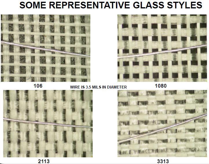
119

120 What to do when you need a stack up with impedance requirements: Additional information: - Final thickness 1.6mm Size: 110 x 70mm - Single ended 50 ohms, routing on Layer 1, 2, 4, 7, 9 & ohms differential, routing on layer 4 and 7. - Prefered min track width is 0.127mm. Your Manufacturer will supply you a build.
121 Changes in physical parameters will affect impedance as follows: As Physical Values Change Impedance Will Move Dielectric Constant (DK) Dielectric Thickness ( h ) Line Width ( w ) Line Thickness ( t )


122 Effect of variables on impedance value. We can take a simple strip-line configuration, vary one element at a time, and calculate the resulting value.


123 Thickness of coating will influence on impedance coating is often excluded on RF applications
124 What to do when you need a stack up with impedance requirements: (Cont d) Feed back from manufacturer should be: - Complete stack up, BOM. - Track width to use on the impedance traces - Space to use between the impedance traces - Calculation result Make your critical tracks visible and easy to find - Use a dedicated D-Code for these traces
125 BASIC Two major applications areas, RF/analog and Digital The major differences between these two areas are the ability of the PCB involved to tolerate signal losses and the complexity of the PCB. RF/Analog applications are characterized by the need for low dielectric losses, low leakage, a need for a low and uniform dielectric constant followed by a low layer count. Further, since this type of PCB tends to be small, cost of the dielectric material has less effect on overall product cost than on other components. As a result, using more exotic /expensive materials to meet performance goals is acceptable. For this class of PCB, choosing a material based on it s Dk characteristics and Df losses usually dominates over other considerations.
126 Digital applications are characterized by high layer counts, a large numbers of drilled /plated holes, can have buried / blind and small via holes. The processing costs associated with registering, laminating/bonding many layers, drilling and plating ease, usually dominate the choice of materials. Absolute dielectric constant value of the insulating material is important, but less important than processing costs and dimensional stability. As a result, woven glass reinforced materials are nearly always required. The choice of resin system used with the glass reinforcement is made based on keeping Z-axis expansion within acceptable limits. The thicker the PCB is, the higher the Tg must be to produce a reliable PCB. Digital applications are nearly always subjected to pricing pressures, so material choices must be made to just achieve performance requirements without adding extra cost.
127 Material Property Comparison between E-Glass and NE-Glass The primary component of most fiberglass yarns is E-glass, S-glass, or NE-glass. E-glass or electronic glass is the primary glass used in yarns that are used to construct fiberglass fabrics, and is the least expensive among the three. S-glass is generally used for non-electrical applications. NE-glass has improved electrical and mechanical performance over E-glass and is typical used in the Nelco SI and N SI highperformance laminate product lines.
128 Skew traces that are neither parallel nor intersecting with the glass pattern - Altera recommends that you pay close attention to the skew/fiber weave effect for high-speed data rates of Gbps and up. - For identical dielectric materials, wider traces in general show less susceptibility to fiber weave skew compared to narrow traces. - If possible, use a dense weave (2116) rather than a sparse weave such as 106 or 1080 where this effect is predominant. - For marginal cost increase 25%, move to a better laminate such as Nelco made of NE-glass (lower Er) compared to the regular E-glass (higher Er). Altera Corporation is a Silicon Valley manufacturer of PLDs, reconfigurable complex digital circuits
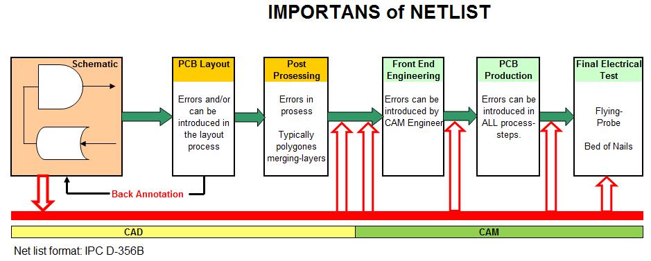
129 Skew traces that are neither parallel nor intersecting with the glass pattern - Plan the routing on the board in such a way that the routing ends up being at an angle rather than orthogonal. - Make use of zig-zag routing. The trace can be routed so that it traverses a minimum of 3 times the fiberglass pitch before reversing the direction of routing. The drawbacks is the increase in board real estate along with the difficulty associated with routing at arbitrary routing angles other than the typical 0, 45, and 90, 2014 Josse: Changes in materials will help on, eliminate skew
 for a")

130 Designers should pay close attention to the layout and the dielectric materials in the PCB design. At high frequencies, dielectric loss is dominant, and is dependent on the dissipation factor (loss tangent) for a given dielectric material. The orientation of the trace with respect to the glass weave determines the amount of skew seen, due to the fiber weave glass pattern. Prepregs that are more homogeneous, eg 3313 are available, and more will come..
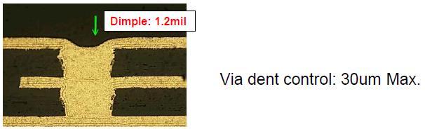
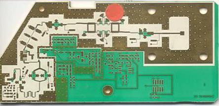
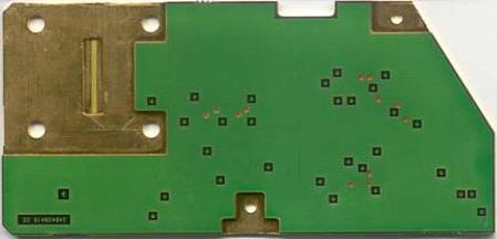
 - 12 layer board, board size: 300 X 240mm - The board is a high frequency RF board with an embedded component between layer 3 and 4.")
131 S A M P L E The embedded component. Size is 130 x 30mm RF Board with embedded component (Filter) - 12 layer board, board size: 300 X 240mm - The board is a high frequency RF board with an embedded component between layer 3 and 4. The side to side alignment between the 2 figures on layer 3 and 4 is critical. Alignment must be within +/-25um. Due to a military confidential design, the illustrations shown here is not the original ones.
132
133 Backdrilling A B C D Drilling Electroless & PP Back-drilling Finished Product

134 More S A M P L E s 1/2 Advanced Multilayer build Material: TU-752 TG 180, Dk: 4.3 / 1GHz Dk4.1 / 10GHz Calculated with Dk 3.8 All copper layers, 1.0oz (35um) Look at line width/space for 50 ohm ss

135 More S A M P L E s 2/2 Advanced Multilayer build Material: TU-752 TG 180, Dk: 4.3 / 1GHz Dk4.1 / 10GHz Calculated with Dk 3.8 All copper layers, 0.5oz (17um) Look at line width / space for 50 ohm ss

136 Another S A M P L E 1/1 Advanced Multilayer build To be creative: Alternative ref. layer has been suggested for the 75ohm single impedance lines on layer 1, 5, 12 and 16.

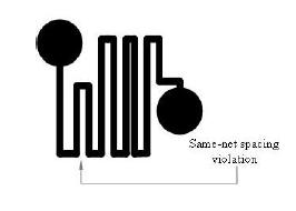
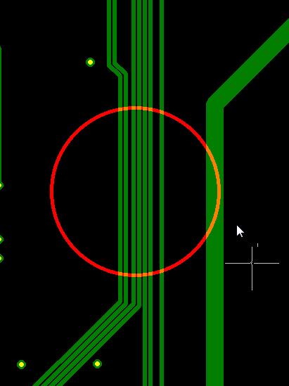
137 Crasy?..not any longer
138 Sample on how an error can occore EVEN if a netlist is attached with original data, or netlist is generated from the PCB Manufacturers CAM system.


139 All mvia connections are of dog-bone type, except one


140 Supplied build - Actual build


141 IPC 4761 Type V: Filled via Specification A via with material applied into the via targeting a full penetration and encapsulation of the hole. Requirements Illustration All holes shall be blocked and hole wall shall be 100% covered with solder mask Dents are acceptable as long as the hole-wall is covered with solder mask or plugging ink Boards with exposed copper or surface finish inside via holes could be rejected. To secure 100 % covering of hole-wall the filling level should be minimum 70% Via hole as a function of the specified stack up IPC 4761 Type VII: Filled and capped via Specification A Type V via with a metalized coating applied over the via (illustration). The metalized capping shall be applied from both sides. Requirements Illustration Thickness of copper plating inside via shall meet the requirement for normal through via according to IPC class 2 unless a stricter requirement is specified in the procurement documentation.cap plating shall be in accordance to IPC 6012C Fig 3.16 and table 3-10 class 3: Copper thickness: Minimum 12 um -Dimples over resin filling maxium 76um -Bumps/protrusion over resin filling maximum 50 um Via hole as it should have been specified in the stack up

142
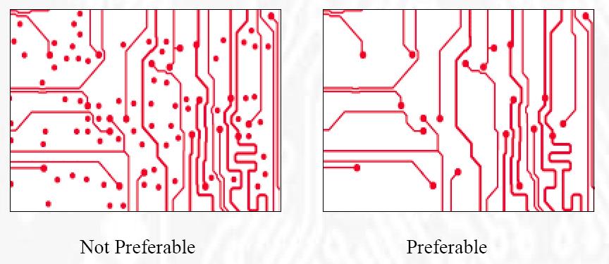
143
144
145
146
147 Some errors seen

148 Same net spacing
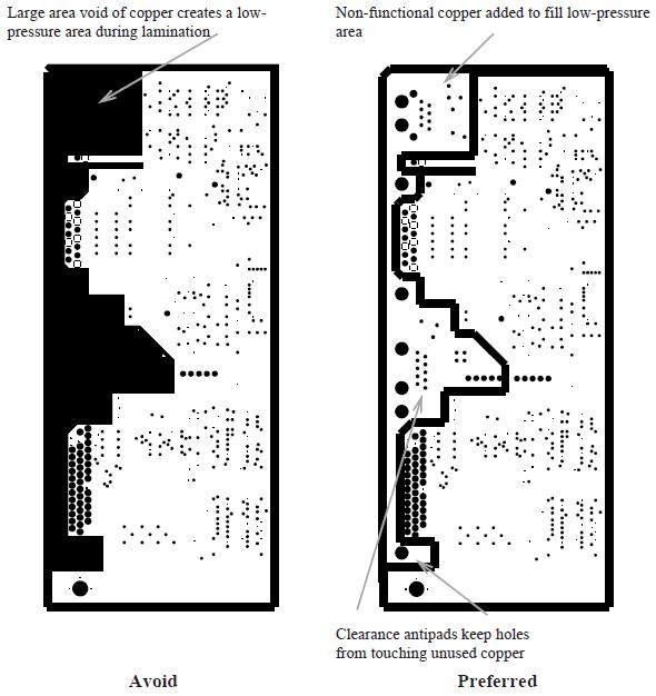
149 Power/Ground Plane Clearance and Thermal Pads Avoid thermal isolation & slivers of copper

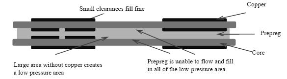
150 Clearance Pads Avoid thermal isolation & slivers of copper
151 Direct Connect Vias (No Thermal Pad) Direct connection of holes to a plane should include a clearance anti-pad half of the diameter of the hole placed at these locations. This will reduce the amount of copper that needs to be drilled, and will result in less drill breakage of smaller drills.
152 Voltage Plane Separation


153 Crosshatch Keep crosshatched drawn areas as vertical and horizontal lines. Do not run them at 45 degrees. These may flake off during processing, and may cause scrap, rework, and false design rule violations in CAM. All over preferred keep the planes solid!

154 Layer 2 Unessesary dence packing of tracks unbalanced

155

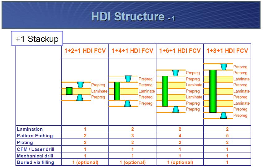
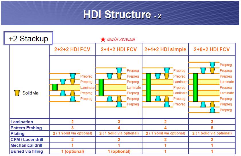
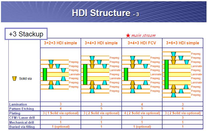
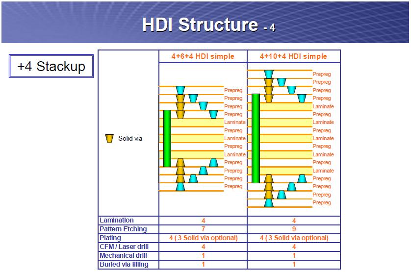
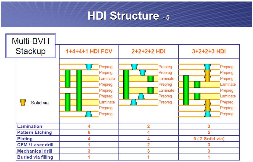
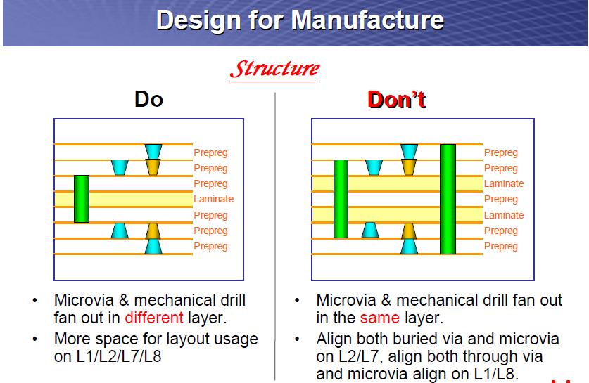
156 --before Rounded corners on Sqare & rectangulare SMD Pads? Why not? --after
157 Layer 5 unbalanced

158 before By adding a ring around the fiducials, you will both tell it is a fiducial and also secure the shape of it. after


159 There will always be room for cleaning up.


160 The following is showing some DFM on a 18 layer Flex Rigid PCB Cu balance layer 01 & 18


161 Cu balance layer 14 & 16 More copper can be added on innerlayers to improve balancing. Better stability ref. bow & twist, - less risk delamination due to low preassure areas.


162 Layer 06 & 08 Signals can be more evenly spread over the flex


163 Same pos. shown on 4 innerlayers Lay 06 Lay 08 Lay 10 Lay 12 <- Layer 06. It is all about cleanup..


164 Both are from Lay 17: Just to make sure that I keep the distance to a absolute minimum.
165
166

167 Advanced HDI PCBs, - microvia holes, - stacked and staggered, - buried vias and buried holes.

168 HDI TECHNOLOGY OVERVIEW
169 HDI Advantages boardsize reduction PCB reduction Layer reduction Although PCB price will increase by adding Microvias, the total system costs can be reduced.
170 HDI Advantages Increasing Fan-out No lost routing space on innerlayers. More routing space between pads. Less risk during soldering process on; solder-bridge solder paste flow away through via holes. Advanced electrical properties Shortest possible connection Advanced thermal properties Thermal Microvias
171 High Density Interconnect Through hole microvia High Inductance Lower Inductance

172 High Density Interconnect Dual head Laser - UV copper ablating laser - CO 2 Dielectric ablating laser Microvia under 800x magnification


173 HDI Microsection Lay up structure: Lay up structure:

174 HDI Microsection Lay up structure:
175
176
177
178
179

180
181

182
183

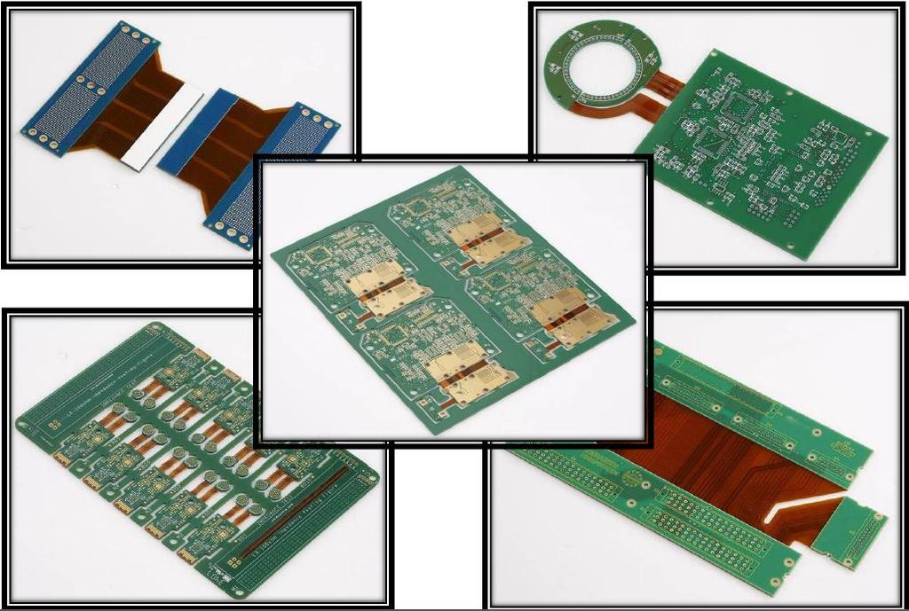
184
185
186
187

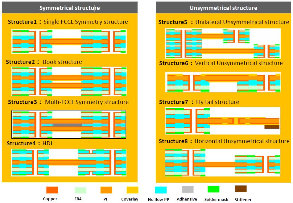
188
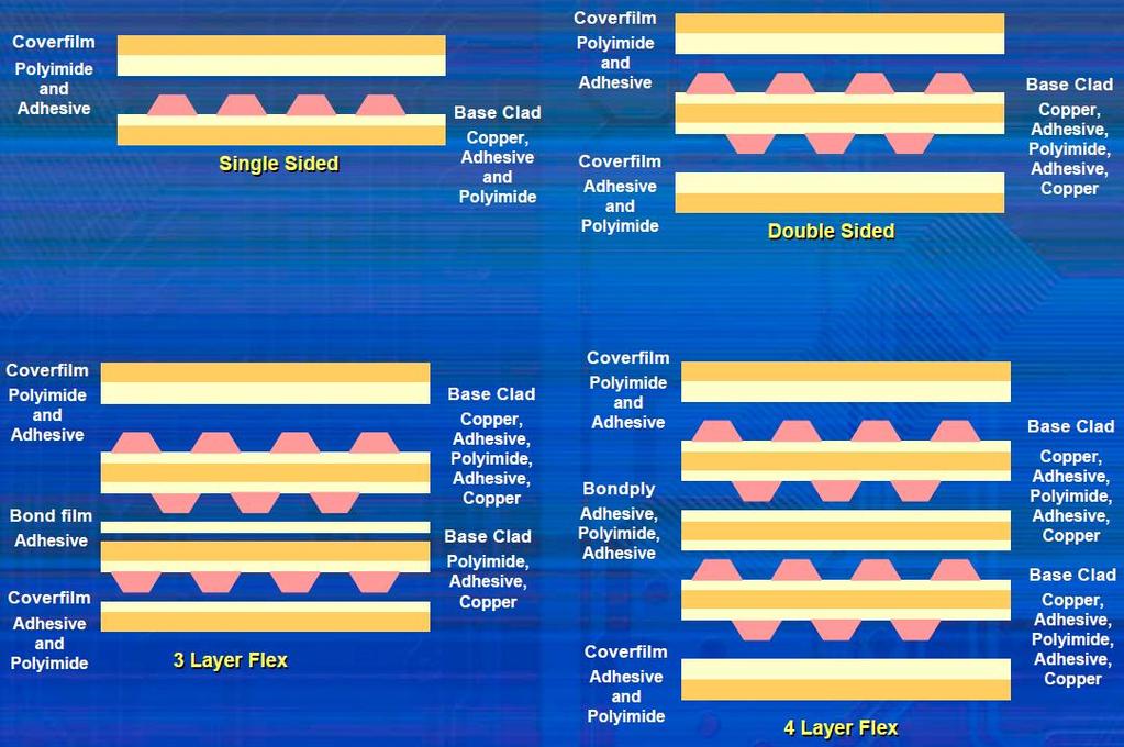
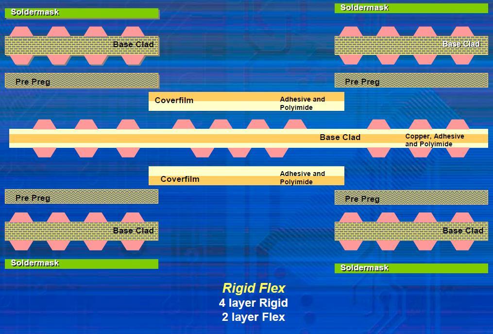
189
190
191
192
193
194
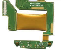
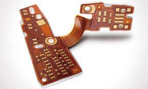
195 - Introduction to Flexible and FlexRigid PCBs

196
197
198 Why Consider Flex? Smaller, smaller, smaller A reduction in space within the design. This affects both size and weight of the overall assembly. By replacing hard wiring you increase the reliability and now deliver a robust design package. The assembly requires a dynamic flex cycle. Flex can be custom designed to achieve impedance requirements. You can improve heat dissipation and allow more air flow inside the box. Folding is required. Folding, forming and component assembly can take place all in one platform.
199 Application Types Static: Not meant to flex Flex to Install or bend and stay: Only meant to flex on limited basis. To install or replace and repair. Dynamic: Depending on flex construction and conditions this could result in >1M flex cycles. Application Attributes Controlled Impedance, by altering material thicknesses you can achieve impedances typically in the ohm range, with a tolerance of 5 10%. Depending on construction you can affect flexibility and limit the dynamic characteristics.
200 Application Attributes Cont d Single Sided Flex: Dual Access Flex: (Back Bared Flex) This is a single copper layer/polyimide clad construction with a polyimide/adhesive coverlayer laminated to one side to allow access on one side only. This is the same construction as single sided flex but openings are created in the base polyimide/adhesive layers to allow access to the copper on both sides. Double Sided Flex: This is a dual copper clad consisting of two layers of copper separated by adhesive and polyimide. Plated through holes (vias) complete the continuity from layer to layer. Multilayer Flex: Rigid Flex: This is a combination of single sided and double sided clads to achieve the total layer count desired. Vias are incorporated to connect all layers. This can be single or multiple layers of flex sandwiched between standard PCB materials to create rigid and flexible portions.
201

202 Application Attributes Cont d
203
204
 41,0 μm Bonding Sheet 25,0 μm Coverlay 37,5 μm 3L Base Cu 17,5 μm Base PI (Polyimide + Adhesive) 94,0 μm 4L Base Cu 17,5 μm Coverlay 37,5 μm No flow PRE-PREG 65,0 μm FR-4 CORE 500,0 μm 5L")
205 LAYER SPECIFICATION Tickness 1L Copper foil 35,0 μm Total 5 (7) rigid layers And 3 flex layers FR-4 CORE 500,0 μm No flow PRE-PREG 65,0 μm Coverlay 37,5 μm 2L Base Cu 17,5 μm Base PI (Polyimide + Adhesive) 41,0 μm Bonding Sheet 25,0 μm Coverlay 37,5 μm 3L Base Cu 17,5 μm Base PI (Polyimide + Adhesive) 94,0 μm 4L Base Cu 17,5 μm Coverlay 37,5 μm No flow PRE-PREG 65,0 μm FR-4 CORE 500,0 μm 5L Copper foil 35,0 μm
206 Design Tips For first time designers and engineers it is a good idea to become familiar with all specifications that govern Flex Circuit manufacturing. IPC ( IPC-2223 and IPC6013 How do you want your flex to act or perform? Develop your schematic. Layer counts and trace densities will be calculated Identify power, signal and ground traces Understand your current requirements Calculate conductor width needs
207 Flex Circuit Related Specifications IPC-2223 IPC-600 Sectional Design Standard for Flexible Printed Boards This specification has the most comprehensive tips for creating your design. This presentation is based on this specification. Manufacturability and Acceptability of Printed Circuits IPC-FC-231 Flexible Bare Dielectrics for use in Flexible Printed Wiring IPC-FC-232 Adhesive coated dielectric films for use in cover sheets for Flexible Printed Wiring IPC-FC-233 Flexible Adhesive Bonding Films IPC-FC-241 Metal clad flexible dielectric for use in fabrication of Flexible Printed Wiring IPC-4562 IPC-T50-D Metal Foil for Printed Wiring Applications Terms and definitions definitions
208 Material selection Attributes to consider flexibility, impedance, emi, to name a few. Thinner material does not equate to cheaper. In most cases the thinner the copper and or polyimide/adhesive, the more expensive it is. Component termination method Surface mount, through hole, etc Level of electrical testing needed to assure that your design is acceptable. Open and short test Full functional test of all components
209 - Your ultimate design is a collaboration across multiple engineering disciplines, Electrical, Mechanical and CAD. Paper Doll- This term is used in conjunction with mechanical mock ups. This is a cost effective way of demonstrating form and fit and in most cases a good safety net to catch potential mechanical issues. Trace/Space- While this is one of the building block of your design, special care must be given to the actual trace structure. Care must be taken to avoid sharp corners more typical of a PCB design
210 Tear Stops- All inside corners MUST have a radius. In these cases a tear stop should be incorporated into the design as an added safety feature to guard against tearing or cracks propagating across a flex circuit. Shields and Planes- Cross hatching can be used to create a shield or plane when flexibility is still a requirement. Shields can be created using copper or they can be screened on using conductive silver epoxy. Grain Direction- When designing dynamic flex the copper grain direction must be taken into account. Rolled Annealed copper has a specific grain direction. To maximize the copper life you must flex in the direction of the grain.


211 Material Utilization- This is the number one cost contributor to your design. When running product, most shops use a panel format. The more up per panel the lower the cost. Your goal should be the smallest form factor as possible. This can be achieved several ways but one of the most creative ways is to incorporate folds into your design. I-Beam- When routing your conductor in a double sided flex it is best to stagger the conductors to prevent an I-Beam effect. With the conductors stacked you run the risk of compression issues when bending to install. Conductor aspect- In a perfect world that rule of thumb is 5 times the conductor thickness. This is a safe rule, however your design will be pushed to ever increasingly smaller trace and space geometries.

212 -Filleted pad/ Hold Down Tabs (Flex-circuits) -A major location for failure in a flex circuit is the interface between the board trace and the pad at the end. It is extremely critical that these interface points have transitional areas more commonly referred to as fillets. Hold down tabs add robustness to the copper pad. The additional hold down tab keeps the pad anchored during any subsequent assembly and rework. - Solder Relief -When placing pads in large copper traces or ground planes, solder relief pads should be created to allow for easier soldering of components. Large copper areas will sink heat away and cause cold or weak solder joints.


213 Electrical Considerations - Predictable electrical characteristics make flex boards an ideal choice for high-speed signal transmission. - Uniform spacing between tracks and grounds, continuous shield layers, and repeatable geometries are features that help control impedance and reduce crosstalk. - With flex boards, you can eliminate connectors and other transitions that contribute to signal attenuation. - Manufacturers can provide tight tolerances on track width, spacing, and distance to ground layers in order to meet your impedance requirements. - Actual impedance will also depend on the board s shape after installation. - Contact your manufacturer for advice on designing boards to specific electrical characteristics.

214 Copper vs. Silver inc. shilding
215 Silver Ink Flex Design Lower cost May be used for economic shielding in EMI sensitive applications - May be used over two or three layer copper flex for additional shielding in Mil/Aero applications Single-Ended Applications - Use below 250 MHz Differential Applications - Use below 1 GHz (2 Gbps) Current carrying power and ground should be placed on copper layers Limited flexure cycles
216 Insertion Loss ComparisonInsertion Comparison


217 Bend Radius: Single-layer: 06 board thickness (minimum) Double-layer: 12 board thickness (minimum) Multilayer: 20 board thickness (minimum) Circuit thickness is approximately 0.15mm per layer. Sharper, permanent bends are common for bend and stay applications Strain vs. Ductility: The bending of flex boards causes deformation, strain, and stresses in the circuit materials. The strains and stresses are functionally related for each material via the stress-strain diagram. The forces necessary to cause flexural deformation are small; the flexural deformation is determined by the imposed bend geometry.
218 Polyimide Films. - This is the material used as the base layer for both the copper clad and the coverfilm. The most common thicknesses are: ( Red is less common ) mm mm mm mm mm Adhesives - Adhesives are used to bond the polyimide film to the copper layer or board layer it is exposed to. Some of the typical adhesive types are: Acrylic, Modified Acrylic, Phenolic Butyral, Modified epoxy and PSA (Pressure sensitive adhesives). The most common thicknesses are mm mm mm - When it comes to temperature resistance, the adhesive is typically the performance-limiting element of a laminate, especially when polyimide is the base material. - As with base films, adhesives come in different thicknesses. The thickness selection is typically a function of the application. For example: Different adhesive thicknesses are commonly used in the creation of coverlayers in order to meet the fill demands of different copper-foil thicknesses that may be encountered. It is essential that you verify the chosen material availability from your manufacturer.
219 LAMINATED COVERLAYERS - Normally, a coverlayer is a two-layer material comprised of a base material and a suitable thermosetting adhesive. However, suitable homogenous thermoplastic films may also be used as coverlayers. The coverlayer serves to protect the conductors of the finished flex board and help enhance flexibility. PHOTOIMAGEABLE COVERLAYERS COVERCOATS - Another type of coverlayer for use in flex manufacture is a photoimageable coverlay. This product is akin to dry film solder mask. It requires vacuum lamination to assure a good seal around the board traces. Just like a photoimageable solder mask, the material is exposed and developed to provide access to board component attachment features. - The term covercoat is used to describe a range of thin coatings applied to the surface of conductors in lieu of a coverlayer. Although some suppliers of covercoat material have some impressive flex cycling data, covercoats are normally reserved for applications where no (or minimal) dynamic flexure is required. In manufacturing, covercoats normally are applied as a liquid by screen-printing and then either cured by heat or by exposure to UV radiation.

220 FILLET TRANSITION EDGE OF STIFFENER - Filleting of the transition edge of a stiffener with a resilient adhesive or epoxy is another common method of strain relieving boards. The small bead of a suitable polymer will provide a simple means of transitioning strain from the stiffener to the flex board.
 Annular Ring - This is the exposed copper ring surrounding a through hole.")

221 -Basic Glossary of Terms (see IPC-T50-D for complete list) Adhesive -Acrylic*, flame retardant, epoxy, epoxy prepreg, polyimide prepreg, phenolic ( * most common materials used for manufacturing flex circuitsfor max flexibility.) Annular Ring - This is the exposed copper ring surrounding a through hole. Artwork - This is the tool used to define circuit features. Typically CAD generated. Back Bared Pads - This is a flex that is typically single sided in construction but has the copper accessed from both sides. Back Side Access - This is a flex that is typically single sided in construction but has the copper accessed from both sides. Conductor / Track - The metallic path that carries electrical current.

222 Track / Conductor Spacing - This is the distance between tracks measured at the foot (widest point) of the track. Track Conductor Width - This is the width of the track measured across the base of the track. Coverfilm Dynamic - This is the insulating material, usually in a film format, that is laminated to the flex board to define solderable areas. Can be drilled, laser cut or chemically removed to create complex geometries. - This is the term used to describe the intended use of the flex. Repeated flexing, as in a disk drive, requires a dynamic flex circuit. ED, Electro Deposited -This is the means by which copper is deposited on polyimide to create an adhesiveless clad.


223 Hard Tooling - A term used to describe tooling used to fabricate flex boards typically when tight tolerances and or high volumes are required. HASL -This is the acronym for a soldering process. Hot Air Solder Level. (Often not ideal to use on flex boards) Hold Down Tabs -These are extensions of the copper pad and are used to help anchor the pad during soldering processes both in assembly and rework. I-Beam Effect -This is the result of stacking your conductors during your design. Subsequent flexing induces stress and compression, causing cracking to occur. Impedance - Basically this is the total effective resistance to AC current. It can be altered by changing conductor spacing, signal spacing relative to ground, material thicknesses.


224 Nested Panel - This is the process by which the individual board is maximized on a panel. Pad - The end of a conductor usually configured to accept a component or to be attached to a device. PIC, Photoimagable Coverfilm - This is another means of defining your solderable areas. This material is apply in a clean room environment, exposed with an artwork and then developed. This allows for complex geometries not available from routing or other soft tooling means.

225 Pads only Plate (button plate) -This is the process by which only the via and a small portion of the surrounding pad is plated in a double sided or multilayer flex. This limits the amount of plating a panel will see and allows the double sided flex board to still be somewhat flexible.
 - This is a term used to describe the type of copper and it is actually the method by which the copper is flattened.")
226 PSA (Pressure Sensitive Adhesive) - An adhesive used to bond stiffeners to specific regions of the flex circuit. RA (Rolled Annealed) - This is a term used to describe the type of copper and it is actually the method by which the copper is flattened. Through Hole/Vias - A plated hole in the panel that can be accessed through the coverfilm or can be tented over with the coverfilm. There are numerous versions of these. Blind Via - Typically a via that penetrates to several layers below but is covered up by the coverfilm Buried Via - A via that is set deep inside a multilayer with no access to the coverfilm Tented Via - A via that goes completely though the flex, but is covered by the coverfilm on both end limiting access.
 - 10:1 maximum. Track width /space - Using ½ ounce (17um) thick copper, 0.1mm track/space - Using 1 ounce (35um) thick copper, 0.")
227 Panel size (is manufacturer dependent - Single sided through multilayer construction, 12 x 18 Drilled holes size - Plated or non-plated 0.25mm diameter - Tolerance of hole to hole is ± 0.1mm Aspect ratio (ratio of hole depth/hole diameter) - 10:1 maximum. Track width /space - Using ½ ounce (17um) thick copper, 0.1mm track/space - Using 1 ounce (35um) thick copper, 0.15mm track/space Conductor aspect ratio - For best producibility, design traces to be at least four times as wide as they are thick. In tight situations it can be successful to achieve : 1 ratio conductor widths. Layer count layers - Solid or cross hatched ground layers
228 Stiffener - Epoxy-glass (FR-4), polyimide-glass, polyimide, copper, aluminum. Surface finishes - ENIG - Chemical Tin - Chemical Silcer - Hard Gold over Nickel - HASL / LF-HASL **** - OSP Outline tolerances: - SRD 0.38mm - Laser / Hard tool 0.10mm - CMD (chemical Milled die) 0.25mm Shield layers - Solid or grid patterned - copper foil or screened conductive ink. **** Do not use it..due to blowing in the wind and extreme process temperature.


229 Fingers - Supported: 0.20mm minimum, center-to-center; - Unsupported: 0.50mm minimum, center-to-center.
230 TEAR-RESISTANCE FEATURES IN FLEX DESIGN - All flex board designs should be made as tear-resistant as possible. While the material may not be intrinsically tear-resistant, tear-resistance can be improved by employing certain features in the design. There are several possible methods, described and illustrated below. All of the following techniques have been successfully used to help prevent tearing. One or more of the following techniques can be used: 1) Radius All Internal Corners The first line of defense against tearing is to make certain that all internal corners are provided with as generous a radius as possible. This design practice is the most important and simplest of all methods used to prevent tearing of the flex buard material.
231 2) Laminate Glass Fabric in Corners Glass cloths can be laminated into corners during the fabrication process. Though not flexible, this method has been shown to provide a very robust corner construction and has been favored in the past by military product designers. It is an expensive solution, however, because of the type of preparation required and should be used only after careful consideration of the alternatives. Use Fluoropolymer Coverlayer The use of fluoroplastics such as Teflon as coverlayers helps to improve tear resistance by virtue of the high tear resistance of the polymer itself. This is due to the fact that fluoropolymer tends to stretch rather than tear, adding toughness to the substrate. An additional benefit of using fluoropolymer coverlayers for those involved in high frequency design is that the dielectric constant of the coverlayer is much lower.
232 3) Use of Radiused Slots The use of slots with ends that have a radius to access relieved board features also can serve to provide tear resistance. Normally, such features can easily be provided for during the punching operation or other board fabrication process. 4,5) Drilled Holes at Corners or Ends of Slits Drilled or punched holes in corners or at the ends of access slits have been used with success when flexible appendages must be spaced close together. This method allows the greatest use of material, but the hole size chosen will impact tear resistance. If the hole is very small, the overall robustness will be reduced.
233 6) Aramid Fibers Inside Cut Line As an alternative to glass cloth, the use of aramid fibers routed through corners or along the entire outline of the flex board is a unique method to stop tearing. The thin polymer fibers have very high strength and are very pliable, minimally affecting flexibility. However, this is a labor intensive method and should only be specified with the knowledge of cost impact. 7) Leave Metal in Corners The board design should, if possible, have small areas of copper provided for at internal corners to serve as tear stops at the inside of corner radius. This serves to prevent further or imminent propagation of a tear through the polymer, should a tear in the material start.
234 (1)Large radius in corner (2)Embedded glass cloth (3)Radiused slot (4)Hole in slit (5)Drilled hole at corner (6)Embedded aramid fiber (7)Extra copper in corner

235 Proper circuit nesting can greatly improve panel yield and lower overall cost. If folding can be tolerated as an assembly operation, yield can be maximized. For dynamic flex board designs, the grain direction requirement may impact layout.


236 It is best to specify round (instead of slotted), through-holes. This will reduce drillingtime and cost. Whenever possible, design pads larger than the access holes. If space is critial, use hold-down tabs. Hold-down tabs are especially important for single layer boards, because a single layer board does not have the added strength of plated through-holes. A variety of hold-down tab designs are available. Pad fillets improve etched yield and material strength. Fillets are appropriate when the pad diameter is greater than the connecting strand width. Acute angles at the interface between traces and pads are to be avoided by using fillets to minimize the concentration of stress at the interface.


237 The steel rule die is a cost-effective tool for punching flex boards from their panel. Class-A tooling for flex circuit punching offers both high precision and long tool life. Example of an etched punch die tool


238 STAGGERED LENGTH BOARDS (BOOKBINDER CONSTRUCTION) For ease of flexing multilayer and rigid flex designs, the use of staggered length design is commonly employed. The technique is accomplished by adding slightly to the length of each succeeding flex layer, moving away from the bend radius. Staggered length designs facilitate bending of the flex board. The circuit can only be bent in one direction by design. A common rule of thumb is to add length equal to roughly 1.5 times the individual layer thickness. Without staggered lengths, layer buckling occurs.

239 - Design issues.cont d Various flexing and bending methods large radius or hinge type flex Coiled flex Counter Rolling flex window shade flex Accordion flex Rolling flex

240 Example materials for various requirements Flexible applications There is no universal base material for printed circuit boards. Whether for standard applications, HF, high temperature or other applications: A large number of substrate types is available. For further technological questions concerning circuit boards, please contact your Elmatica team.

241 The information for the chart are taken from a sample of circuits built with standard materials. This chart is not intended to be used as a price guide. However, it does showthat circuit cost generally rises with layer count. It is in your best interest to consider all options to minimize cost. For example, use two circuits to do the job of one. Two double-layer circuits may be less expensive than one four-layer circuit. But the cost savings of the circuit may be offset by additional assembly requirements. Circuits can also be folded in order to save space and layers. Each situation is unique. A rela-tively small amount of time invested in project assessment canresult in significant savings overall.
242
243

244 Introduction to MB PCB Metal Back PCB s. Aluminium for Power and LED applications.
245 Metal Back Technologies

246 Aluminum Core PCB for LED application Aluminum is superior in heat conduction, corrosion resistance, lightweight and cost.

247 Metal Back Technologies Types

248 Metal Back Adhesive

249 Metal Core
Welcome to Streamline Circuits Lunch & Learn. Design for Reliability & Cost Reduction of Advanced Rigid-Flex/Flex PCB Technology
 Welcome to Streamline Circuits Lunch & Learn Design for Reliability & Cost Reduction of Advanced Rigid-Flex/Flex PCB Technology Accurate PCB data is critical to the tooling process. Here are some key items
ALTIUMLIVE 2018: NAVIGATING THE COMPLEXITIES OF PCB MATERIAL SELECTION
 ALTIUMLIVE 2018: NAVIGATING THE COMPLEXITIES OF PCB MATERIAL SELECTION Chris Hunrath Insulectro, VP of Technology San Diego October 4 Outline 1 PCB Material Overview 2 What is the Dielectric Constant of
Flex and Rigid-Flex Printed Circuit Design
 Flex and Rigid-Flex Printed Circuit Design Old Content - visit altium.com/documentation Modified by on 29-Nov-2016 Related Videos Bending Lines Enhanced Layer Stack Management Layer Stack Regions A rigid-flex
GRAPHIC MANUFACTURING CAPABILITY Q217-18
 All features are design dependent and may not be achievable in combination Reduced Yield / Special values up ( or down ) to the standard limit are design and application dependent Standard features only
Deepen your knowledge
 FLEX & RIGID-FLEX PRINTED CIRCUIT BOARDS Deepen your knowledge What are Flex & Rigid-flex Printed Circuit Boards? What are their similarities and differences? Their capabilities? And the design rules.
Qualification and Performance Specification for High Frequency (Microwave) Printed Boards
 Printed Boards") Qualification and Performance Specification for High Frequency (Microwave) Printed Boards Developed by the High Speed/High Frequency Board Performance Subcommittee (D-22) of the High Speed/High Frequency
Qualification and Performance Specification for High Frequency (Microwave) Printed Boards Developed by the High Speed/High Frequency Board Performance Subcommittee (D-22) of the High Speed/High Frequency
!"#$#%&#'(() ) **+,-./01)2-,-.3)456,1) /0! **)
 ) **+,-./01)2-,-.3)456,1) /0! **)") !"#$#%&#'(() ) **+,-./01)2-,-.3)456,1) /0!7.5853-09**) B 2 IT is a Toshiba Process Technology 1. Conductive Ag bumps are printed on a sheet of Cu foil. 2. Prepreg is pierced through by the bumps 3. Another
!"#$#%&#'(() ) **+,-./01)2-,-.3)456,1) /0!7.5853-09**) B 2 IT is a Toshiba Process Technology 1. Conductive Ag bumps are printed on a sheet of Cu foil. 2. Prepreg is pierced through by the bumps 3. Another
Qualification and Performance Specification for Flexible Printed Boards
 Qualification and Performance Specification for Flexible Printed Boards Developed by the Flexible Circuits Performance Specifications Subcommittee (D-12) of the Flexible Circuits Committee (D-10) of IPC
Bending Impacts Layers
 Designing for Flexibility and Reliability Understanding factors that contribute to the reliability of a flex circuit that is formed or repeatedly flexed The name "flexible circuit" sums up the function
ATS Document Cover Page
 221-008 Item Rev Status: RELEASED printed 9/20/2017 2:27:42 PM by Les Deenin ATS: OPERATIN PROCEDURE ATS Document Cover Page Responsible Department: Supply Chain This copy is uncontrolled unless otherwise
Stackup Planning, Part 1
 by Barry Olney coulmn BEYOND DESIGN Stackup Planning, Part 1 The PCB substrate that physically supports the components, links them together via highspeed interconnects and also distributes highcurrent
How Printed Circuit Boards are Made. Todd Henninger Field Applications Engineer Midwest Region
 PCB 101: How Printed Circuit Boards are Made Todd Henninger Field Applications Engineer Midwest Region Tooling PRE-PRODUCTION ENGINEERING (Tooling) Design Data Package CAD Data (ODB++ or Gerber 274x format)
Flex-Rigid Design Guide
 DESIGN GUIDE Version 1.2 / March 2018 Flex-Rigid Design Guide The trend to miniaturization in electronics continues. Integrated circuit board solutions are becoming more and more popular as a means of
Building HDI Structures using Thin Films and Low Temperature Sintering Paste
 Building HDI Structures using Thin Films and Low Temperature Sintering Paste Catherine Shearer, James Haley and Chris Hunrath Ormet Circuits Inc. - Integral Technology California, USA chunrath@integral-hdi.com
IPC-2221B APPENDIX A Version 2.0 June 2018
 IPC-2221B APPENDIX A Version 2.0 June 2018 A.1 INTRODUCTION This appendix was developed by the IPC 1-10c Test Coupon and Artwork Generation Task Group and is included in this current document revision
Multek s lead free compatible and compliant material selection February 01, 2006
 Multek s lead free compatible and compliant material selection Helmut.Kroener@de.multek.com +49 7 463 543 February 0, 2006 Overview I. Introduction II. Project setup III. Tested materials IV. Test vehicle
UL PCB Recognition what is it & why do you need to know about it
 UL PCB Recognition what is it & why do you need to know about it Presented by Emma Hudson NCAB Customer Event March 2015 UL and the UL logo are trademarks of UL LLC 2015 Agenda What is UL and what are
FLEXIBLE & RIGID-FLEX CIRCUITS TECHNICAL ENGINEERING GUIDE. Delivering Quality Since 1952.
 FLEXIBLE & RIGID-FLEX CIRCUITS TECHNICAL ENGINEERING GUIDE Delivering Quality Since 1952. DELIVERING QUALITY SINCE 1952. Epec Engineered Technologies designs and manufactures customized, built-to-print,
Nine Dot Connects. DFM Stackup Considerations Part 4 Webinar August The following questions were asked during the webinar.
 DFM Stackup Considerations Part 4 Webinar August 2015 The following questions were asked during the webinar. Question / Comment Aren't the inner signal layer traces classified as embedded micro-strips
Low CTE / High Tg FR-4 with High Heat Resistance
 Low CTE / High Tg FR-4 with High Heat Resistance Laminate: EM-827 Prepreg: EM-827B 1 Features Tg(DSC) > 170 Z direction CTE < 3.0% (50~260 ) High thermal degradation temperature: Td > 340 Excellent thermal
14. Designing with FineLine BGA Packages
 14. Designing with FineLine BGA Packages S51014-1.0 Chapter 14, Designing with FineLine BGA Packages, replaces AN 114: Designing with FineLine BGA Packages. Introduction As programmable logic devices (PLDs)
ThunderClad 2. TU-883 HF Very Low Loss Material. Laminates & Prepregs Mass Lamination Service Insulated Metal Substrate Materials
 ThunderClad 2 TU-883 HF Very Low Loss Material Laminates & Prepregs Mass Lamination Service Insulated Metal Substrate Materials TUC Product Roadmap 2 ULVP VLP HCF Ultra Low Void Prepreg Very Low Profile
Modeling Printed Circuit Boards with Sherlock 3.2
 Modeling Printed Circuit Boards with Sherlock 3.2 DfR Solutions September 23, 2014 Presented by: Dr. Nathan Blattau Senior Vice President 9000 Virginia Manor Rd Ste 290, Beltsville MD 20705 301-474-0607
B-IS400 IS420/3 IS400 IS420 PCL370HR. Temperature resistant mid and high T g - base materials with low z-axis expansion CAF ENHANCED
 J B-IS4 IS42/3 IS4 IS42 PCL37HR Temperature resistant mid and high T g - base materials with low z-axis expansion CAF ENHANCED Temperature-resistant base materials with low z-axis expansion IS4, IS42 and
Chapter 14. Designing with FineLine BGA Packages
 Chapter 14. Designing with FineLine BGA Packages S53009-1.3 Chapter 14, Designing with FineLine BGA Packages, replaces AN 114: Designing with FineLine BGA Packages. Introduction As programmable logic devices
The Anatomy of a PCB SINGLE-SIDED BOARD
 Published on Online Documentation for Altium Products (https://www.altium.com/documentation) 主页 > The Board Using Altium Documentation Modified by Jason Howie on Apr 11, 2017 Open up just about any electronic
New Developments in PCB Laminates. Dean Hattula, John Coonrod Rogers Corporation Advanced Circuit Materials Division
 New Developments in PCB Laminates Dean Hattula, John Coonrod Rogers Corporation Advanced Circuit Materials Division Overview PCB laminate properties Thermal stability Electrical performance Summary PCB
How to select PCB materials for highfrequency
 How to select PCB materials for highfrequency apps Find out how to simplify that choice when striving for the best tradeoff between ease of fabrication and best electrical performance. By John Coonrod
Company Overview Markets Products- Capabilities
 Company Overview Markets Products- Capabilities A Simpler way for PCB production. www.purepcb.co.uk What can Pure do for you? From 1 off Circuit upward, No MOQ/MOV High Mix Production Focus. Fast Turn
Interconnection Reliability of HDI Printed Wiring Boards
 Presented in the ECWC 10 Conference at IPC Printed Circuits Expo, SMEMA Council APEX and Designers Summit 05 Interconnection Reliability of HDI Printed Wiring Boards Tatsuo Suzuki Nec Toppan Circuit Solutions,
High Layer Count PCB. Technology Trends in KOREA ISUPETASYS
 High Layer Count PCB Technology Trends in KOREA April, 21 2011 Sang Soo LEE ISUPETASYS Contents 2 Definition of High Layer Count PCB Core Technology Trends High Layer Count PCB Technology Drivers Interconnection
Flexible Printed Circuits Design Guide
 www.tech-etch.com/flex Flexible Printed Circuits Design Guide Multilayer SMT Assembly Selective Plating of Gold & Tin-Lead Fine Line Microvias Cantilevered & Windowed Leads 1 MATERIALS CONDUCTOR Copper
ICDs (InterConnect Defects) What are they? Where do they come from? How can we make them go away? Doug Trobough Suixin Zhang
 What are they? Where do they come from? How can we make them go away? Doug Trobough Suixin Zhang") ICDs (InterConnect Defects) What are they? Where do they come from? How can we make them go away? Doug Trobough Suixin Zhang Definition of ICD ICDs are any defect that occurs adjacent to the innerlayer
ICDs (InterConnect Defects) What are they? Where do they come from? How can we make them go away? Doug Trobough Suixin Zhang Definition of ICD ICDs are any defect that occurs adjacent to the innerlayer
IMPACT OF MICROVIA-IN-PAD DESIGN ON VOID FORMATION
 IMPACT OF MICROVIA-IN-PAD DESIGN ON VOID FORMATION Frank Grano, Felix Bruno Huntsville, AL Dana Korf, Eamon O Keeffe San Jose, CA Cheryl Kelley Salem, NH Joint Paper by Sanmina-SCI Corporation EMS, GTS
Taconic Advanced Dielectric Division. Thomas McCarthy. Sean Reynolds. Jon Skelly
 Strategies for Designing Microwave Multilayer Printed Circuit Boards Using Stripline Structures Taconic Advanced Dielectric Division Thomas McCarthy Sean Reynolds Jon Skelly Multilayer/Stripline Design
FABRICATING HIGH CURRENT, HEAVY COPPER PCBS
 Royal Circuit Solutions 21 Hamilton Ct, Hollister, CA 95023 (831) 636-7728 www.royalcircuits.com FABRICATING HIGH CURRENT, HEAVY COPPER PCBS INTRODUCTION All printed circuit boards (PCBs) carry current
PCB Fabrication Specification
 Original Author: Steve Babiuch Process Owner: Steve Babiuch Page 2 of 8 1.0 Purpose This specification establishes the NEO Tech fabrication requirements for printed circuit boards. The order of precedence
IPC Qualification and Performance Specification for Organic Multichip Module (MCM-L) Mounting and Interconnecting Structures IPC-6015
 Mounting and Interconnecting Structures IPC-6015") ASSOCIATION CONNECTING ELECTRONICS INDUSTRIES Qualification and Performance Specification for Organic Multichip Module (MCM-L) Mounting and Interconnecting Structures February 1998 A standard developed
ASSOCIATION CONNECTING ELECTRONICS INDUSTRIES Qualification and Performance Specification for Organic Multichip Module (MCM-L) Mounting and Interconnecting Structures February 1998 A standard developed
High Frequency Circuit Materials Attributes John Coonrod, Rogers Corporation
 High Frequency Circuit Materials Attributes John Coonrod, Rogers Corporation Specialty high frequency circuit materials have been used in the PCB industry for decades and for many different reasons. There
Sherlock 4.0 and Printed Circuit Boards
 Sherlock 4.0 and Printed Circuit Boards DfR Solutions January 22, 2015 Presented by: Dr. Nathan Blattau Senior Vice President 9000 Virginia Manor Rd Ste 290, Beltsville MD 20705 301-474-0607 www.dfrsolutions.com
IPC-6012DA with Amendment 1. Automotive Applications Addendum to IPC-6012D Qualification and Performance Specification for Rigid Printed Boards
 A with Amendment 1 Automotive Applications Addendum to Qualification and Performance Specification for Rigid s FINAL DRAFT FOR INDUSTRY REVIEW MAY 2018 0.1 Scope This addendum provides requirements to
CANDOR Industries Inc. High Quality PCB Manufacturing Solutions
 CANDOR Industries Inc High Quality PCB Manufacturing Solutions 1 Our Mission Founded in 1999, Candor is an industry leader in High Technology Printed Circuit Board Fabrication Services. Quick turn services
Verifying The Reliability Of Connections In HDI PWBs
 Verifying The Reliability Of Connections In HDI PWBs The stacking of via holes is used effectively in the development of high density circuits on build-up printed wiring boards (PWBs). However, when micro
PCB Production Process HOW TO PRODUCE A PRINTED CIRCUIT BOARD
 NCAB Group Seminars PCB Production Process HOW TO PRODUCE A PRINTED CIRCUIT BOARD NCAB GROUP PCB Production Process Introduction to Multilayer PCBs 2 Introduction to multilayer PCB s What is a multilayer
Innovative PCB Solutions. Win time and flexibility benefit from Swiss quality. THE PCB CHALLENGE Doing it together
 Innovative PCB Solutions Win time and flexibility benefit from Swiss quality THE PCB CHALLENGE Doing it together INDIVIDUAL CUSTOMER SOLUTIONS from a reliable partner 2 Optiprint offers consulting, development
Freescale Semiconductor Tape Ball Grid Array (TBGA) Overview
 Overview") Freescale Semiconductor Tape Ball Grid Array (TBGA) Overview Revision 0 2006 Freescale and the Freescale logo are trademarks of Freescale Semiconductor, Inc. All other product or service names are the
Freescale Semiconductor Tape Ball Grid Array (TBGA) Overview Revision 0 2006 Freescale and the Freescale logo are trademarks of Freescale Semiconductor, Inc. All other product or service names are the
Manufacturing Capacity
 Capability List Manufacturing Capacity QTA & Prototype Layer : 1L ~32 L Impedance Board Ball Grid Array ( BGA ) Blind/ Buried Via Micro Via ( Laser Drilling) Flex /Rigid Flexible PCB Series Orders Layer
Pad Crater Project Definition Stage. Joe Smetana Alcatel-Lucent For Member Meeting 2/9/2011 San Jose, CA
 Pad Crater Project Definition Stage Joe Smetana Alcatel-Lucent For Member Meeting 2/9/2011 San Jose, CA The issue(s) Pad Cratering defects are a significant challenge with Pb-free PCB materials and/or
DURAVER -E-Cu quality 104 ML
 J B-DE 104 ML DURAVER -E-Cu quality 104 ML Base materials for multilayers 2 Quality and security to give you the edge The demands imposed with regard to the performance of circuit boards are rising constantly,
Technology Aluminium-IMS-PCBs Rev For latest information please visit
 Options and Characteristics Online calculation On explicit enquiry Quantity 1 piece up to 1,0² total area from 1 piece to mass production Layer quantity 1- and 2-layers up to 6 layers Material thickness
Basic 4-layer manufacturing process
 Basic 4-layer manufacturing process Erwin Lemmens - AQC BV 7-11 D&E BE / Booth 1 8-11 D&E NL / Booth 18 AQC (Advanced Quality Control) BV Supplying pcb s, flex, flex-rigids, aluminium, etc - standard and
Flex and Rigid flex boards. 02/2013 Written by Zreik Anan
 Flex and Rigid flex boards 02/2013 Written by Zreik Anan Advantages Better Reliability Dynamic flexing Replace cables (Static Flexing) Simplify assembly process Less rework Saves money Materials Flex clad
The Essential Role of DFx In The Lean Smart New Product Introduction (NPI) Flow
 Flow") The Essential Role of DFx In The Lean Smart New Product Introduction (NPI) Flow Presenter: Michael Ford Title: Marketing Development Manager Date: 16 th March 2017 Today s Agenda What is Industry 4.0 and
The Essential Role of DFx In The Lean Smart New Product Introduction (NPI) Flow Presenter: Michael Ford Title: Marketing Development Manager Date: 16 th March 2017 Today s Agenda What is Industry 4.0 and
Trends and Developments
 Trends and Developments Monique Mayr Monique.Mayr@eu.panasonic.com European R&M Group Panasonic Corporation Electronic Material Business Division Weitere Informationen finden Sie auch auf: http://www3.panasonic.biz/em/pcbm/en/index.html
ALTIUMLIVE 2018: FLEX: SOMETHING NEW FOR EVERYONE
 ALTIUMLIVE 2018: FLEX: SOMETHING NEW FOR EVERYONE Tara Dunn Omni PCB President San Diego October 5, 2018 Applications That Span Technology Today s Discussion: 1. Basic processing steps for both subtractive
Technology HF-Printed Circuits Rev For latest information please visit
 Options and Characteristics Online calculation On explicit enquiry Quantity 1 piece up to 0,4m² total area from 1 piece to mass production Layer quantity 1 to 2 layers Up to 8 layers Material thickness
DESIGNCON High Speed Signal Path Losses as Related to PCB Laminate Type and Copper Roughness
 DESIGNCON 2013 High Speed Signal Path Losses as Related to PCB Laminate Type and Copper Roughness Lee Ritchey, Speeding Edge Leeritchey@speedingedge.com John Zasio, Speeding Edge Zasio@pacbell.com Rich
Measuring Copper Surface Roughness for High Speed Applications
 Measuring Copper Surface Roughness for High Speed Applications John A. Marshall MacDermid Inc. 245 Freight Street Waterbury CT, USA Abstract This paper examines the use of Light Interferometry and the
c/bach, 2-B Pol. Ind Foinvasa Montcada i Reixac (Barcelona) SPAIN Tel FAX
 SPAIN Tel FAX") 1- What is 2- How does it work? 3- How do we make it? 4- Applications 5- Processing? WHAT IS? Thick aluminium based substrate, cladded in ED copper foil. Designed for an effective thermal dissipation and
1- What is 2- How does it work? 3- How do we make it? 4- Applications 5- Processing? WHAT IS? Thick aluminium based substrate, cladded in ED copper foil. Designed for an effective thermal dissipation and
Advanced Material Selection IPC Designers Council. Michael J. Gay February 8 th 2017
 Advanced Material Selection IPC Designers Council Michael J. Gay February 8 th 2017 Michael.gay@isola-group.com Laminate Material Components Resin, Glass, Copper Resin Glass Copper Prepreg or B-Stage B-Stage
VT-45PP VT-47PP VT-447PP
 & Prepreg General Information Ventec provides a series of and Prepregs with different glass style and resin content. These products have good bonding and thermal performance in applications of heat sink
RO4835T Core/RO4450T Bonding Layers Multi-Layer Board Processing Guidelines
 Fabrication Technical Articles Notes RO4835T Core/RO4450T Bonding Layers Multi-Layer Board Processing Guidelines These guidelines were developed to provide fabricators basic information on processing core
Annular Ring and Feature Clearances. Track to Feature Clearances
 Hi-Tech Corporation Technical Capabilities Annular Ring and Feature Clearances Outer Value layer min (mm) A 75 B 125 C 150 Inner Value layer min (mm) A 100 B 150 C 150 Track to Feature Clearances Outer
Introduction Conductors. Supply Planes. Dielectric. Vias PCB Manufacturing Process Electronic Assembly Manufacturing Process
 PCBs/Overview Printed Circuit Boards (PCB) Introduction Conductors. Supply Planes. Dielectric. Vias PCB Manufacturing Process Electronic Assembly Manufacturing Process 29/09/2005 EE6471 (KR) 263 PCBs/Overview
PEC (Printed Electronic Circuit) process for LED interconnection
 process for LED interconnection") PEC (Printed Electronic Circuit) process for LED interconnection Higher wattage LED s/ power components or their placement in higher densities, requires a larger dissipation of heat in a more effective
PEC (Printed Electronic Circuit) process for LED interconnection Higher wattage LED s/ power components or their placement in higher densities, requires a larger dissipation of heat in a more effective
Process & Capability Manual (Vol )
") Process & Capability Manual (Vol. 12-2015) Seite 1 von 13 1 CHAPTER OVERVIEW 1 CHAPTER OVERVIEW... 2 2 MICROCIRTEC A SHORT PROFILE... 3 2.1 WHO WE ARE... 3 2.2 OBJECTIVES & MARKETS... 3 2.3 DECLARATION
Process & Capability Manual (Vol. 12-2015) Seite 1 von 13 1 CHAPTER OVERVIEW 1 CHAPTER OVERVIEW... 2 2 MICROCIRTEC A SHORT PROFILE... 3 2.1 WHO WE ARE... 3 2.2 OBJECTIVES & MARKETS... 3 2.3 DECLARATION
A Novel Material for High Layer Count and High Reliability Printed Circuit Boards
 A Novel Material for High Layer Count and High Reliability Printed Circuit Boards Jie Wan, Junqi Tang, Xianping Zeng Shengyi Technology Co., Ltd. No.5 Western Industry Road, North Industry District SSL
Question: Are RO4000 materials compatible with lead-free processes? Answer:
 Question: Are RO4 materials compatible with lead-free processes? Answer: RO4 cores and prepregs are among the most temperature stable products available. They easily meet or exceed all expectations for
(13) PCB fabrication / (2) Focused assembly
 PCB fabrication / (2) Focused assembly") Company Fact Sheet TTM Technologies, Inc. is a world-wide leader in the manufacture of technologically advanced PCBs, backplane and sub-system assemblies. Our Global Presence / Local Knowledge approach
Company Fact Sheet TTM Technologies, Inc. is a world-wide leader in the manufacture of technologically advanced PCBs, backplane and sub-system assemblies. Our Global Presence / Local Knowledge approach
Flexible PCB Plating Through Hole Considerations, Experiences and Solutions
 Presented in the ECWC 10 Conference at IPC Printed Circuits Expo, SMEMA Council APEX and Designers Summit 05 Flexible PCB Plating Through Hole Considerations, Experiences and Solutions Neil Patton Atotech
The Effects of Board Design on Electroplated Copper Filled Thermal Vias for Heat Management
 The Effects of Board Design on Electroplated Copper Filled Thermal Vias for Heat Management Carmichael Gugliotti, Rich Bellemare MacDermid Enthone Electronics Solutions Waterbury, CT, USA Richard.bellemare@macdermidenthone.com
LTCC SYSTEMS and LTCC DESIGN RULES
 LTCC SYSTEMS and LTCC DESIGN RULES Low Temperature Co-fired Ceramic revision status: G page 1 of 19 Table of Contents: 1 General page 3 2 Commercial LTCC tape systems page 4 3 Design possibilities page
Designing With High-Density BGA Packages for Altera Devices. Introduction. Overview of BGA Packages
 Designing With High-Density BGA Packages for Altera Devices December 2007, ver. 5.1 Application Note 114 Introduction As programmable logic devices (PLDs) increase in density and I/O pins, the demand for
Embedded Passives..con0nued
 Embedded Passives..con0nued Why Embedded Passives? Improves the packaging efficiency System-on-Package (SOP); SLIM integration Reducing size Eliminating substrate assembly Minimizing solder joint failure
B-DE104. DURAVER -E-Cu quality 104 quality 104 KF quality 104 TS
 J B-DE104 DURAVER -E-Cu quality 104 quality 104 KF quality 104 TS Epoxy fibre glass laminate (FR-4) Circuit boards for computers, communications systems, industrial electronics and electronic devices in
B-IS620i/3. IS620i. Base material. for high-frequency. applications CAF. Enhanced
 J B-/3 Base material for high-frequency applications CAF Enhanced Low loss base material with a stable dielectric behaviour over frequency is a base material for high frequency applications, especially
Taconic Advanced Dielectric Division. Thomas McCarthy. Sean Reynolds. Jon Skelly
 Strategies for Designing Microwave Multilayer Printed Circuit Boards Using Stripline Structures Taconic Advanced Dielectric Division Thomas McCarthy Sean Reynolds Jon Skelly Multilayer/Stripline Design
12 Technical Paper. Key words: PPR electroplating, via fill, thermal management, through hole fill
 12 Technical Paper The Effects of Board Design on Electroplated Copper Filled Thermal Vias for Heat Management Carmichael Gugliotti, Rich Bellemare MacDermid Enthone Electronics Solutions Waterbury, CT,
Design and Construction Affects on PWB Reliability Paul Reid PWB Interconnect Solutions
 Design and Construction Affects on PWB Reliability Paul Reid PWB Interconnect Solutions The reliability, as tested by thermal cycling, of printed wire boards (PWB) are established by three variables; copper
LEAD-FREE ASSEMBLY COMPATIBLE PWB FABRICATION AND ASSEMBLY PROCESSING GUIDELINES.
 LEAD-FREE ASSEMBLY COMPATIBLE PWB FABRICATION AND ASSEMBLY PROCESSING GUIDELINES. TECHNICAL BULLETIN As the industry has moved to lead-free assembly processing, the performance demands on the lead free
3M Electromagnetic Compatible Products
 3M Electromagnetic Compatible Products Selection Guide Revision E 3 Innovation Faster, smaller, lighter, easier the skyrocketing development of today s electronics requires new solutions for significant
Specification for Base Materials for Rigid and Multilayer Printed Boards
 ASSOCIATION CONNECTING ELECTRONICS INDUSTRIES Specification for Base Materials for Rigid and Multilayer Printed Boards Developed by the Laminate/Prepreg Materials Subcommittee (3-11) of the Printed Board
NP-180R NAN YA PLASTICS CORPORATION ELECTRONIC MATERIALS DIVISION. COPPER CLAD LAMINATE DEPARTMENT NO TUNG HWA N. ROAD, TAIPEI, TAIWAN.
 New: 2014/04/30 flame retardant copper clad laminate NP-180R High Tg 175 (DSC) Excellent dimensional stability through-hole reliability Excellent electrical, chemical and heat resistance properties IPC-4101C
MATERIALS. September Construction Profiles and Material Decomposition p.18. Improved Thin-Film Resistor Material p.24
 September 2013 Construction Profiles and Material Decomposition p.18 MATERIALS Improved Thin-Film Resistor Material p.24 High-Frequency Laminates for Hybrid Multilayer PCBs p.30 Material Selection for
Implementation of IECQ Capability Approval using the IPC-6010 series of Standards
 Page 1 of 13 INTERNATIONAL ELECTROTECHNICAL COMMISSION QUALITY ASSESSMENT SYSTEM FOR ELECTRONIC COMPONENTS (IECQ) DOCUMENT NUMBER: OD 301 DOCUMENT TYPE: Operational Document VERSION: Version 1 TITLE: Implementation
- 1 - Contents. Date: Date changed Made by: PCB Technical. Accepted by: Gordon Falconer
 - - page of 4 Contents Inner and outer layer features... 2. Description... 2.2 Capability... 2 2 Build-up / Multilayer... 3 2. Common capability... 3 Standard build-up... 3 3 Drilling/Routing/V-cut/Bevel...
ESA s approach to quality control of the supply chain for PCBs. Stan Heltzel European Space Agency
 ESA s approach to quality control of the supply chain for PCBs Stan Heltzel European Space Agency Outline A. ESA s approach to supply chain control for PCBs B. Case study: contamination in PCBs 1. Problem
Thermal image of 0603 capacitor at the center of a microstrip (47pF/250V/C0G) assembled on RF-35TC under 200 watts applied power.
 assembled on RF-35TC under 200 watts applied power.") offers a "best in class" low dissipation factor with high thermal conductivity. This material is best suited for high power applications where every 1/10 th of a db is critical and the PWB substrate is
offers a "best in class" low dissipation factor with high thermal conductivity. This material is best suited for high power applications where every 1/10 th of a db is critical and the PWB substrate is
Mastering the Tolerances Required by New PCB Designs. Brad Hammack Multek Doumen, China
 Mastering the Tolerances Required by New PCB Designs Brad Hammack Multek Doumen, China Abstract The packaging industry is driving the Printed Circuit Board (PCB) technology level in the direction of semiconductor
Why Flex? Capabilities. Why PCi?
 Why Flex? Innovation Flexible circuits give you a unique tool to bring your innovative packaging ideas to market, and to separate your products from the crowd. Flex gives you the ability to create circuitry
PRINTED CIRCUITS HANDBOOK
 PRINTED CIRCUITS HANDBOOK Clyde F. Coombs, Jr. Sixth Edition Me Graw New York Chicago San Francisco Lisbon London Madrid Mexico City Milan New Delhi San Juan Seoul Singapore Sydney Toronto CONTENTS List
Lead Free Assembly: A Practical Tool For Laminate Materials Selection
 Lead Free Assembly: A Practical Tool For Laminate Materials Selection Erik J. Bergum David Humby Isola Abstract: The impending European RoHS legislation, restricting the use of lead containing solders,
TEST REPORT (Self-Tested Data)
") TEST REPORT (Self-Tested Data) CLIENT: IPC Validation Services 3000 Lakeside Drive Suite 105N Bannockburn, IL 60015 USA Attention: Mr. Randy Cherry +1-847-597-5606 TEST ITEMS: Peel Strength, Volume Resistivity,
TEST REPORT (Self-Tested Data) CLIENT: IPC Validation Services 3000 Lakeside Drive Suite 105N Bannockburn, IL 60015 USA Attention: Mr. Randy Cherry +1-847-597-5606 TEST ITEMS: Peel Strength, Volume Resistivity,
NiP Resistor Manufacturing Overview
 0 NiP Resistor Manufacturing Overview Thin film NiP resistive alloy material is made by electrodepositing of the NiP alloy onto copper foil (RESISTOR-CONDUCTOR MATERIAL) which is then laminated to a dielectric
PAD CRATERING. Chris Hunrath VP of Technology Integral Technology Lake Forest, California THE INVISIBLE THREAT TO THE ELECTRONICS INDUSTRY
 PAD CRATERING THE INVISIBLE THREAT TO THE ELECTRONICS INDUSTRY Presented by Chris Hunrath VP of Technology Integral Technology Lake Forest, California IPC-9708 What is Pad Cratering? 1.2.4 Pad Cratering