ME 141B: The MEMS Class Introduction to MEMS and MEMS Design. Sumita Pennathur UCSB
|
|
|
- Christian Reynolds
- 6 years ago
- Views:
Transcription
1 ME 141B: The MEMS Class Introduction to MEMS and MEMS Design Sumita Pennathur UCSB
2 Outline Class odds and ends Intro to Your Device Process Flow for Your Device Microfabrication Outline
3 Suggested groups Group 1 Group 2 Group 3 Group 4 Group 5 Simon Bill Gina Adam Dustin Chavez Peter Herbert Jared Frey Charles Garcia Hong Li Tyler Hatlen Steven Wehmeyer Brian Hoffman Group (6) Group (7) Group (8) Group (9) Group (10) Jarred Hare Ludovico Megalini Louis VanBlarigan Travis O Donnell Burga Kaytanli Ashok Kodigala Christian Gebbe Miguel Zepeda- Rosales Tyler Ray Yuhui Ma 9/28/10 3/45
4 Safety Lecture! Thursday 12:30-2:15pm MANDATORY ATTENDANCE Lithography/cleaning training next week Sign up on sheet Groups 1&6, 2&7, 3&8, 4&9, 5&10 attend trainings together Let me know ASAP if you need to change groups 9/27/10 4/45
5 Lab Report Information You will be learning how to make a specific device, and in the process you will have 3 lab reports due Lab Report I due 10/19 Individual Lab Reports must be turned in, but do the work with your lab partner Must be professional quality work! Remember, this is the bulk of your grade 9/27/10 5/45
6 Outline Class odds and ends Intro to Your Device Process Flow for Your Device Microfabrication Outline
7 Outline to your Device 1. Etching Channels 1. Solvent clean 2. Spin photoresist 3. Expose with opposite of the fluidic pattern 4. Develop photoresist 5. Deposit hard mask (Cr-Au) 6. Lift off 7. Wet etch (Buffered HF) 8. Metal etch 2. Depositing Electrodes 1. Solvent clean 2. Spin photoresist 3. Expose with metal pattern (aligned to fluidic features) 4. Develop photoresist 5. Descum 6. Evaporate Ti-Au 7. Lift off 3. Sealing the Channels 1. Prepare Flat PDMS (3-5mm Thick) 2. Punch holes (biopsy punch) 3. Clean 4. O 2 Plasma Treatment 5. Align and Bond 6. Run experiments
 Evaporate Hard Mask")

8 Etching Channels Solvent Clean Sample Develop PR Spin Photoresist (PR) Evaporate Hard Mask (Cr-Au) Expose Sample Lift Off Orange: Exposed, Red: Unexposed Etch Channel Then Remove Metal

")
9 Depositing Electrodes Solvent Clean Sample Orange: Exposed PR Red: Unexposed PR Spin Photoresist (PR) Develop PR Evaporate Metal (Ti-Au) Expose Sample Lift Off


10 Sealing the Channels Prepare Flat PDMS Align Biopsy Punch Access Holes Bond Fill with Fluid O 2 Plasma Surface Treatment Perform Experiments
11 Process odds and ends Mask 2 (electrodes) will be given to you Mask 1 you must design yourself and print out on a transparency Substrates will be provided to you. Be wise with them! Next Week: Cleaning substrates, Lithography, inspection If you finish channel by Week 6, you may design and fabricate your own microfludic/nanofluidic device Otherwise, focus on creating perfect micro/nano device Weeks 8-10: Characterization and testing of devices. You MUST have a working device by then! 9/27/10 11/45
12 Microfabrication Outline Substrates Si, SOI, Fused quartz, etc.. Lithography and patterning Doping Thin Films Etching Wafer Bonding Surface Micromachining Process Integration 9/27/10 12/45
13 Substrates: Silicon Silicon is a diamond-structure cubic crystal Comes with different amount of either n-type or p- type doping 9/27/10 13/45

14 SOI Silicon wafers with embedded layers, such as silicon-oninsulator (SOI) wafers Initial purpose: build IC s on device layer, and buried oxide minimized stray capacitance to substrate Common MEMS purpose: bulk micromachining top layer into moveable structures with well-controlled thickness 9/27/10 14/45
15 Other substrates Glass (cheap, high impurity content) Inexpensive base for soft lithography Transparent for optical access Can be very strongly attached to silicon wafers via anodic bonding Quartz/Fused silica Compound semiconductors Optical applications Plastics PDMS Titanium Sapphire Strong, wear resistant, transparent, insulating substrate Compatible with CMOS (so transparent CMOS MEMS) Expensive, hard to etch 9/27/10 15/45
16 Substrate Summary 9/27/10 16/45
17 Microfabrication Outline Substrates Si, SOI, Fused quartz, etc.. Lithography and patterning Doping Thin Films Etching Wafer Bonding Surface Micromachining Process Integration 9/27/10 17/45

18 Optical Lithography 9/27/10 18/45


19 Methods of optical lithography I Contact Mask touches wafer Inexpensive Contact degrades mask No die size limit Resolution: down to 1 micron nervously; down to several microns comfortably Proximity Mask of order 10 microns from wafer Inexpensive Less mask damage Diffraction means lower resolution No die size limit Resolution: down to several microns nervously, somewhat larger comfortably 9/27/10 19/45
20 Projection Lithography Projection lithography, especially when combined with an optical imaging system that reduces the image size, is used for high-resolution patterning (submicron to very submicron) Larger mask features, no contact with mask Wafer steppers expose one die at a time, assuring good focus and registration Something to consider: if your device needs a fine features, a stepper may be required. But steppers have limits on dies size of about 1 cm. 9/27/10 20/45

21 Positive thin resist Spin cast Thickness of order 1 micron Developer removes exposed resist Creates sloped profile at resist edge Some applications Wet etching Shallow Dry Etching Front end standard 9/27/10 21/45

22 Spin cast Negative/image reversal Thickness of order 1 micron Developer removes unexposed resist Creates a re-entrant profile Typical application: liftoff processes (in acetone), often seen in back end processing Rule of thumb: resist thickness should be 3x thickness of layer to be lifted off Not a standard front end material, but not inherently incompatible with it photoresists 9/27/10 22/45
23 Details that matter for lithographic processing Existing topography: if your existing feature heights are comparable to or greater than the thickness of the resist that you are putting down, you will not have good coverage Incompletely covered sidewalls, holds full of resist, resist that never enters a hole at all Solutions: eliminate the topography, thicker resist, alternate coating technology (spray on, electrophoretic resist?), use of a previously patterned hard mask instead of a resist mask Patterned resist does not have a square profile can affect the topography of whatever you pattern with the resist Resist adhesion If the surface of the wafer is hydrophilic (like SiO2), the resist might peel during subsequent wet processing steps. Surface preparation is key (e.g. dehydration bake and HMDS coating to render surface hydrophobic) 9/27/10 23/45
24 Cleaning! When we say (for example) that positive thin resist is compatible with front end processing, we do not mean that you can have resist on your wafer during most of the front-end process! Must remove resist and clean wafer thoroughly before any high temperature processes Always include cleaning in process flows, starting at the crayon engineering level Resist removal techniques O2 plasma ash Chemical removal of organics: piranha clean or nanostrip Solvents (acetone) 9/27/10 24/45

25 More cleaning! 9/27/10 25/45

26 Another important detail: process bias The feature drawn on the mask is NOT the same size as the feature produced on the wafer Exposed area usually extends beyond clear area on mask Resist selection impacts process bias Resist thickness Resist Tone 9/27/10 26/45
27 Design Rules Alignment of one pattern to the next is critical to device fabrication Design rules are created to assure that fabrication tolerances do not destroy devices 9/27/10 27/45
28 Microfabrication Outline Substrates Si, SOI, Fused quartz, etc.. Lithography and patterning Doping Thin Films Etching Wafer Bonding Surface Micromachining Process Integration 9/27/10 28/45
29 Doping Doping is the introduction of a controlled amount of impurities to change the conductivity type and degree of a semiconductor In silicon, boron is a p-type dopant (creating holes), while phosphorus, arsenic, and antimony are n-type dopants (creating conduction electrons) Some doping incorporated in initial silicon melt All modern thin film doping is done with ion implantation Doping doesn t add a new thin film, but it modified the properties of a thin film at the surface of an existing material 9/27/10 29/45
30 Ion Implantation A high-voltage accelerator is used to shoot ions at the wafer The beam must be rastered and the wafer must be rotated to achieve uniform dose Usually a thin protective layer, such as oxide, is used to prevent sputtering of the surface and to reduce channeling The depth of the implant dose depends on energy Activation anneal after implantation allows dopants to reach proper positions in crystal 9/27/10 30/45
31 Effective Range The effective range measures the location of the peak concentration of an implanted species 9/27/10 31/45

32 Masking of implants Control of which regions of a wafer receive the implant is achieved with masking layers 9/27/10 32/45
33 Diffusion After implantation, ions are driven deeper into the substrate by diffusion, a high-temperature process The junction depth is the point at which the implanted ion concentration is equal (but of opposite type) to the substrate doping 9/27/10 33/45
34 Microfabrication Outline Substrates Si, SOI, Fused quartz, etc.. Lithography and patterning Doping Thin Films Etching Wafer Bonding Surface Micromachining Process Integration 9/27/10 34/45
35 Creating thin (and thick) films Many techniques to choose from Differences: Front or back end processes Quality of resulting films (electrical properties, etch selectivity, defects, residual stress) Conformality Deposition rate, cost Physical techniques Material is removed from a source, carried to the substrate, and dropped there Chemical Techniques Reactants are transported to the substrate, a chemical reaction occurs, and the product deposit on the substrate to form the desired film 9/27/10 35/45
36 Taxonomy of deposition techniques Chemical Thermal Oxidation Chemical Vapor Deposition (CVD) Low Pressure (LPCVD), Atomspheric pressure (APCVD), Plasma Enhanced (PECVD) Epitaxy Electrodeposition (Electroplating) Physical Physical Vapor Deposition (PVD) Evaporation Sputtering Spin-casting 9/27/10 36/45
37 Oxidation I Silicon forms a high quality, stable oxide How it works: Oxygen diffuses through oxide to SI/oxide interface SI + O 2 + high temperature (~1100) furnace SiO 2 Some Si is consumed Rate determined by diffusion of oxygen through oxide Diffusion limits practical oxide thickness to < 2 um A key front end process 9/27/10 37/45
38 Oxidation II Dry Oxidation (O 2 ) High quality, slow oxidation rate, smaller maximum thickness (i.e. gate oxide) Wet Oxidation (steam) H 2 to speed the diffusion Lower quality, faster oxidation rate The Deal-Grove model describe the kinetics of oxidation quite well for oxides greater in thickness that about 30nm 9/27/10 38/45
39 The Deal-Grove Model 9/27/10 39/45
40 Local Oxidation Oxidation can be masked locally by an oxidation barrier, such as silicon nitride Oxide undercuts edge of mask layer to form a bird s beak Oxidation followed by an oxide etch can also be used to sharpen silicon features 9/27/10 40/45
41 Chemical Vapor Deposition (CVD) How CVD works: Gaseous reactants, often at low pressure Long mean free path; reactants reach substrate Reactants react and deposit products on the substrate Unlike Oxidation, does not consume substrate material Energy sources facilitate CVD reactions: High temperature, plasma, laser Processing temperatures vary widely Commonly deposited films: Oxide, silicon nitride, polysilicon CVD results depend on pressures, gas flows, temperature Film composition, uniformity, deposition rate, and electrical and 9/27/10 mechanical characteristics can vary 41/45
42 Some reasons to use CVD Oxide formation: To get a thicker layer than thermal oxidation can provide To create oxide on a wafer that can t withstand high temperatures (for example because of metal features) To create oxide on top of a material that is not silicon For film formation in general To tailor the film properties (like form stress) by adjusting pressures, flow rates, external energy supply, ratios of different precursor gases (to adjust proportions of different materials in the final product) Conformailty : (more of less) even coating on all surfaces Drawbacks: Films deposited at low temperature are often lower quality than high temp versions, and have less predictable properties Flammable, toxic or corrosive source gases 9/27/10 42/45
43 Thick Film Formation CVD is a common MEMS tool for creating thick films on the wafer surface In practice, film stress limits thickness (film delamination or cracking, or curvature of underlying structures) Can deposit thick oxides; nitrides are still typically submicron Must anneal deposited oxides for some applications lose low stress property on anneal 9/27/10 43/45

44 CVD enables conformal coating 9/27/10 44/45
45 LPCVD Polysilicon Amorphous at lower deposition temperatures and high deposition rates Typical temperature: ~590 C Polycrystalline at higher deposition temperatures and lower deposition rates Typical temperature: ~625 C Grain size and structure depend on detailed deposition conditions E.g. thicker films larger grains Structure, electrical properties, and mechanical properties also vary with post-deposition thermal processing Grain growth Dpoant activation or diffusion 9/27/10 45/45

46 Polysilicon stress depends on deposition rates 9/27/10 46/45
47 Epitaxy CVD deposition process in which atoms move to lattice sites, continuing the substrate s crystal structure Homoepitaxy: same material, i.e. Si on Si Heteroepitaxy: different materials, i.e. AlGaAs, on GaAs How it happens Slow deposition rate (enough time to find a lattice site) High Temperature (enough energy to move a lattice site) Selective epitaxy is possible through masking Can grow a doped Si layer of known thickness 9/27/10 47/45
48 Electroplating: basics Pass a current through an aqueous metal solution Anode is made of the meta that you want to deposit Cathode is the conductive seed material on your wafer Positive metal ions travel to the negatively charged cathode on your wafer and deposit there Preparing your wafer If you want to plate metal in some places and not in others, you will need a patterned metal seed layer (and typically a sticky metal adhesion layer under that) For very short features, just plate onto the seed layer For taller features, need to plate into a mold Molds can be photoresist, silicon, SU-8, et.. Depending on the needs of your device 9/27/10 48/45
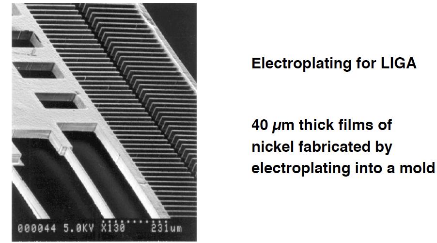
49 Electroplating 9/27/10 49/45

50 Electroplating realities 9/27/10 50/45
 9/27/10 51/45")
51 Conformality and keyholes To lowest order, conformal films coat sidewalls and horizontal surfaces at the same rate But high aspect ratio trenches are prone to keyholes (CVD, electroplating, etc..) 9/27/10 51/45
52 Physical Vapor Deposition Remove materials from a solid source Transport material to substrate Deposit material on substrate Differences among PVD techniques How material is removed from source Directionality when it arrives at substrate Cleanliness of deposition A family of quick, low temperature processes 9/27/10 52/45
53 Thermal Evaporation Source is resistively heated in high vacuum Typical source: metal Hot source atoms are emitted in all directions and stick where they land Substrate receives a directional flux of source material Good for liftoff processes, otherwise poor conformality Possible contamination from generalized heating 9/27/10 53/45

54 E-beam Evaporation Electron beam heats source in high vacuum Typical source: metal Hot source atoms are emitted in all directions and stick where they land Substrate receives a directional flux of source material Good for liftoff processes, otherwise poor conformality Heating is less generalized less contamination 9/27/10 54/45
55 Sputtering Unreactive ions (i.e. Ar) knock material off a target by momentum transfer Targets: metals, dielectrics, piezoelectrics, etc.. Different methods of obtaining energetic ions Magnetron, plasma Low pressure, but not high vacuum Less directional and faster than evaporation 9/27/10 55/45
56 Etching, liftoff, and adhesion layers Films are patterned differently depending on whether the material in question tends to react with other materials Materials that react (for example, aluminum): Deposit a blanket film (sputtering good for better conformality), do photolithography, and etch it into desired shape Materials that don t react readily (for example, noble metals): Hard to etch: typically use liftoff instead Pattern resist, then deposit metal on top with a directional deposition tool Not very sticky: typically need an aehesion layer to stick the noble metal to what lies beneath Example: use a few hundred A thick layer of Cr or Ti to adhere Au to an underlying oxide (deposited without breaking vacuum 9/27/10 between layers) 56/45
57 No! Is that all you can do with deposited films? Spin-casting: put the stuff that you want to deposit in a liquid, spin it onto the surface like resist, and bake out the solvent (spin on glass, PZT piezoelectrics) Other forms of vapor deposition designed for a particular purpose (depositing the inert polymer parylene by vapor deposition followed by polymerization) Lamination of free-standing resist films onto surfaces Self assembled monolayers 9/27/10 57/45
58 Microfabrication Outline Substrates Si, SOI, Fused quartz, etc.. Lithography and patterning Doping Thin Films Etching Wafer Bonding Surface Micromachining Process Integration 9/27/10 58/45
59 Etching Wet Etching Isotropic Anisotropic (for crystals only) Dry etching using plasma reactors Isotropic plasma etching at relatively high gas pressures Anisotrpoic reaction-ion etching at relatively lower gas pressures Sputter etching or ion-beam milling Not very selective A useful reference (what etches what and how fast): Williams, Gupta, an Wasilik, Etch Rates for Micromachining Processing Part II, JMEMS 12, (2003). 9/27/10 59/45
60 Considerations for etching Isotropic Etch rate the same in all crystal directions Anisotrpoic For wet etches, rate depends on crystal plane For dry etches, directionality determined by process Selectivity Etch rate of substrate vs. etch rate of mask Mask Adhesion (for wet etching) Increased etching along mask/substrate interface Temperature Reaction rate limited? Stirring Mass transfer limited? 9/27/10 60/45
61 Isotropic Etching Etch rate is independent of orientation Isotropic etch profile Assume a well-adhered mask with infinite selectivity Mask undercut, rounded etch profile Applications Flow channels Removal of sacrificial layers in surface micromachining 9/27/10 61/45
62 Isotropic etching Some wet etches: Si mixture of nitric, acetic, and HF SiO 2 buffered HF (BOE), also HF vapor SiN hot phosphoric acid PolySi KOH Al PAN etch (phosphoric, acetic, nitric acids) Some dry etches: Si XeF 2 vapor Organics O 2 plasma Mostly clean enough for front enf, with the exception of KOH, which is a contamination risk for very high T processes. XeF 2 vapor is often used as a final release etch 9/27/10 62/45
63 Anisotrpoic wet etching Depends on having a singe-crystal substrate The effect depends on the different etch rates of different exposed crystal planes Silicon etchants for which <111> planes etch slowly Strong bases (KOH, NaOH, NH 4 OH) TMAH Ethylene diamine pyrochatechol Hydrazine 9/27/10 63/45

64 Making a Trench with KOH A rectangular patter is aligned to a [110] direction on a <100> silicon wafer 9/27/10 64/45
65 Making a V-groove The previous etch is allowed to go to termination, i.e. the slowing of etch rate with only {111} planes are exposed (can also make square, pyramidal) 9/27/10 65/45
 plane to stop on 9/27/10 66/45")
66 Convex Corners Convex corners become undercut, as there is no single slowetching (111) plane to stop on 9/27/10 66/45

67 Corner Compensation To etch a convex corner with KOH, add extra material at corner Amount of material is chosen so that it will etch away just when the overall etch reaches the desired depth Extra material protect convex corner from attack 9/27/10 67/45

68 Arbitrary Shapes Any mask feature, if etched long enough, will result in a V-groove tangent to the mask along <110> directions 9/27/10 68/45
![Misalignment Misalignment of the mask relative to the [110]](/docs-images/72/67721000/images/69-2.jpg "direction always results in a larger etched region 9/27/10")
69 Misalignment Misalignment of the mask relative to the [110] direction always results in a larger etched region 9/27/10 69/45
70 Selectivity and etch masks for KOH etches Deep etches are long selectivity matters Mask must last long enough to bring the etch to completion Sidewall erosion must be at an acceptably slow rate Etch rate of {111} planes is finite but small Condition-dependent, of order 400:1 for {100} rate/{111} rate Etch rate of mask Si:SiO 2 selectivity about 100:1 Si:LPCVD SiN selectivity at least 1000:1 PECVD SiN not effective (low quality) Do NOT use photoresist! 9/27/10 70/45
71 Etch Stops When etching into a wafer to leave a specific thickness of material, it is necessary to have some kind of etch stop Example 9/27/10 71/45
72 Dry (Plasma) Etching At reduced pressure, a glow discharge is set up in a reactive gas environment This produces Ions that can be accelerated by the electric fields at the bounding edges of the plasma so that they strike the surface These can be quite directional in their impact Free radicals (uncharged) that can diffuse to the surface and undergo reaction Etching depends on reaction followed by creation of a gaseous byproduct which is pumped away 9/27/10 72/45
73 Applicability Most materials can be plasma etched Oxide Nitride Silicon Most Metals (not the noble metals) Polymers The art is in achieving suitable selectivity both for masking layers and to layers that ie beneath the layer being etched Known recipes (gas mixtures, plasma conditions) with desired selectivity End-point detection is an important part of best practice when using plasma etching 9/27/10 73/45
74 Shape The higher the pressure, the more isotropic the etch because reactants are scattered many times before reaching the surface (this is called plasma etching) To achieve directional anisotropy, one must go to low pressure to achieve long mean-free paths for the ions (this is called reactive-ion etching or RIE) Deep reactive ion etching is another thing altogether 9/27/10 74/45
75 Deep reactive Ion Etching (The Bosch Process) Photoresist mask: selectivity about 50:1 Oxide Mask: selectivity > 100:1 9/27/10 75/45
76 Depth depends on features and layout Features of difference width etch at different rates (recipe dependent) 9/27/10 76/45

77 Multi-level Etching Making multi-level etches can be challenging For through etches with two different depths, simply etch from both sides of wafer, with double-sided alignment 9/27/10 77/45
 features on the same side of the wafer requires a nested mask 9/27/10")
78 Multi-level etching with nested masks Etching two sets of deep (> about 10 um) features on the same side of the wafer requires a nested mask 9/27/10 78/45

79 DRIE with Etch Stop SOI substrate Buried oxide acts as an etch stop Charging can led to footing 9/27/10 79/45
ME 141B: The MEMS Class Introduction to MEMS and MEMS Design. Sumita Pennathur UCSB
 ME 141B: The MEMS Class Introduction to MEMS and MEMS Design Sumita Pennathur UCSB Outline today Introduction to thin films Oxidation Deal-grove model CVD Epitaxy Electrodeposition 10/6/10 2/45 Creating
6.777J/2.732J Design and Fabrication of Microelectromechanical Devices Spring Term Solution to Problem Set 2 (16 pts)
") 6.777J/2.732J Design and Fabrication of Microelectromechanical Devices Spring Term 2007 By Brian Taff (Adapted from work by Feras Eid) Solution to Problem Set 2 (16 pts) Issued: Lecture 4 Due: Lecture
6.777J/2.732J Design and Fabrication of Microelectromechanical Devices Spring Term 2007 By Brian Taff (Adapted from work by Feras Eid) Solution to Problem Set 2 (16 pts) Issued: Lecture 4 Due: Lecture
Microfabrication for MEMS: Part II
 CL: 6.777J/2.372J Spring 2007, Lecture 2-1 Microfabrication for MEMS: Part II Carol Livermore Massachusetts Institute of Technology * With thanks to Steve Senturia, from whose lecture notes some of these
Metallization deposition and etching. Material mainly taken from Campbell, UCCS
 Metallization deposition and etching Material mainly taken from Campbell, UCCS Application Metallization is back-end processing Metals used are aluminum and copper Mainly involves deposition and etching,
EE 5344 Introduction to MEMS. CHAPTER 3 Conventional Si Processing
 3. Conventional licon Processing Micromachining, Microfabrication. EE 5344 Introduction to MEMS CHAPTER 3 Conventional Processing Why silicon? Abundant, cheap, easy to process. licon planar Integrated
IC/MEMS Fabrication - Outline. Fabrication
 IC/MEMS Fabrication - Outline Fabrication overview Materials Wafer fabrication The Cycle: Deposition Lithography Etching Fabrication IC Fabrication Deposition Spin Casting PVD physical vapor deposition
Today s Class. Materials for MEMS
 Lecture 2: VLSI-based Fabrication for MEMS: Fundamentals Prasanna S. Gandhi Assistant Professor, Department of Mechanical Engineering, Indian Institute of Technology, Bombay, Recap: Last Class What is
Fabrication Technology, Part I
 EEL5225: Principles of MEMS Transducers (Fall 2003) Fabrication Technology, Part I Agenda: Oxidation, layer deposition (last lecture) Lithography Pattern Transfer (etching) Impurity Doping Reading: Senturia,
Lecture 22: Integrated circuit fabrication
 Lecture 22: Integrated circuit fabrication Contents 1 Introduction 1 2 Layering 4 3 Patterning 7 4 Doping 8 4.1 Thermal diffusion......................... 10 4.2 Ion implantation.........................
Fabrication Process. Crystal Growth Doping Deposition Patterning Lithography Oxidation Ion Implementation CONCORDIA VLSI DESIGN LAB
 Fabrication Process Crystal Growth Doping Deposition Patterning Lithography Oxidation Ion Implementation 1 Fabrication- CMOS Process Starting Material Preparation 1. Produce Metallurgical Grade Silicon
PHYS 534 (Fall 2008) Process Integration OUTLINE. Examples of PROCESS FLOW SEQUENCES. >Surface-Micromachined Beam
 Process Integration OUTLINE. Examples of PROCESS FLOW SEQUENCES. >Surface-Micromachined Beam") PHYS 534 (Fall 2008) Process Integration Srikar Vengallatore, McGill University 1 OUTLINE Examples of PROCESS FLOW SEQUENCES >Semiconductor diode >Surface-Micromachined Beam Critical Issues in Process
PHYS 534 (Fall 2008) Process Integration Srikar Vengallatore, McGill University 1 OUTLINE Examples of PROCESS FLOW SEQUENCES >Semiconductor diode >Surface-Micromachined Beam Critical Issues in Process
Chemical Vapor Deposition
 Chemical Vapor Deposition ESS4810 Lecture Fall 2010 Introduction Chemical vapor deposition (CVD) forms thin films on the surface of a substrate by thermal decomposition and/or reaction of gas compounds
Lecture 5: Micromachining
 MEMS: Fabrication Lecture 5: Micromachining Prasanna S. Gandhi Assistant Professor, Department of Mechanical Engineering, Indian Institute of Technology, Bombay, Recap: Last Class E-beam lithography X-ray
Czochralski Crystal Growth
 Czochralski Crystal Growth Crystal Pulling Crystal Ingots Shaping and Polishing 300 mm wafer 1 2 Advantage of larger diameter wafers Wafer area larger Chip area larger 3 4 Large-Diameter Wafer Handling
EE 330 Lecture 9. IC Fabrication Technology Part 2
 EE 330 Lecture 9 IC Fabrication Technology Part 2 Quiz 8 A 2m silicon crystal is cut into wafers using a wire saw. If the wire diameter is 220um and the wafer thickness is 350um, how many wafers will this
The Physical Structure (NMOS)
") The Physical Structure (NMOS) Al SiO2 Field Oxide Gate oxide S n+ Polysilicon Gate Al SiO2 SiO2 D n+ L channel P Substrate Field Oxide contact Metal (S) n+ (G) L W n+ (D) Poly 1 3D Perspective 2 3 Fabrication
The Physical Structure (NMOS) Al SiO2 Field Oxide Gate oxide S n+ Polysilicon Gate Al SiO2 SiO2 D n+ L channel P Substrate Field Oxide contact Metal (S) n+ (G) L W n+ (D) Poly 1 3D Perspective 2 3 Fabrication
EE 330 Lecture 8. IC Fabrication Technology Part II. - Oxidation - Epitaxy - Polysilicon - Interconnects
 EE 330 Lecture 8 IC Fabrication Technology Part II - Oxidation - Epitaxy - Polysilicon - Interconnects Review from Last Time MOS Transistor Bulk Source Gate Drain p-channel MOSFET Lightly-doped n-type
EE 330 Lecture 9. IC Fabrication Technology Part II. -Oxidation -Epitaxy -Polysilicon -Planarization -Resistance and Capacitance in Interconnects
 EE 330 Lecture 9 IC Fabrication Technology Part II -Oxidation -Epitaxy -Polysilicon -Planarization -Resistance and Capacitance in Interconnects Review from Last Time IC Fabrication Technology Crystal Preparation
ECE 440 Lecture 27 : Equilibrium P-N Junctions I Class Outline:
 ECE 440 Lecture 27 : Equilibrium P-N Junctions I Class Outline: Fabrication of p-n junctions Contact Potential Things you should know when you leave Key Questions What are the necessary steps to fabricate
Chapter 3 CMOS processing technology
 Chapter 3 CMOS processing technology (How to make a CMOS?) Si + impurity acceptors(p-type) donors (n-type) p-type + n-type => pn junction (I-V) 3.1.1 (Wafer) Wafer = A disk of silicon (0.25 mm - 1 mm thick),
L5: Micromachining processes 1/7 01/22/02
 97.577 L5: Micromachining processes 1/7 01/22/02 5: Micromachining technology Top-down approaches to building large (relative to an atom or even a transistor) structures. 5.1 Bulk Micromachining A bulk
Mostafa Soliman, Ph.D. May 5 th 2014
 Mostafa Soliman, Ph.D. May 5 th 2014 Mostafa Soliman, Ph.D. 1 Basic MEMS Processes Front-End Processes Back-End Processes 2 Mostafa Soliman, Ph.D. Wafers Deposition Lithography Etch Chips 1- Si Substrate
3. Photolithography, patterning and doping techniques. KNU Seminar Course 2015 Robert Mroczyński
 3. Photolithography, patterning and doping techniques KNU Seminar Course 2015 Robert Mroczyński Critical technology processes Photolithography The aim of this process is to transfer (in the most accurate
Silicon Manufacturing
 Silicon Manufacturing Group Members Young Soon Song Nghia Nguyen Kei Wong Eyad Fanous Hanna Kim Steven Hsu th Fundamental Processing Steps 1.Silicon Manufacturing a) Czochralski method. b) Wafer Manufacturing
Chapter 3 Silicon Device Fabrication Technology
 Chapter 3 Silicon Device Fabrication Technology Over 10 15 transistors (or 100,000 for every person in the world) are manufactured every year. VLSI (Very Large Scale Integration) ULSI (Ultra Large Scale
MEMS Fabrication. Beyond Integrated Circuits. MEMS Basic Concepts
 MEMS Fabrication Beyond Integrated Circuits MEMS Basic Concepts Uses integrated circuit fabrication techniques to make mechanical as well as electrical components on a single chip. Small size 1µm 1mm Typically
Surface Micromachining
 Surface Micromachining Micro Actuators, Sensors, Systems Group University of Illinois at Urbana-Champaign Outline Definition of surface micromachining Most common surface micromachining materials - polysilicon
PROCESS FLOW AN INSIGHT INTO CMOS FABRICATION PROCESS
 Contents: VI Sem ECE 06EC63: Analog and Mixed Mode VLSI Design PROCESS FLOW AN INSIGHT INTO CMOS FABRICATION PROCESS 1. Introduction 2. CMOS Fabrication 3. Simplified View of Fabrication Process 3.1 Alternative
EECS130 Integrated Circuit Devices
 EECS130 Integrated Circuit Devices Professor Ali Javey 9/13/2007 Fabrication Technology Lecture 1 Silicon Device Fabrication Technology Over 10 15 transistors (or 100,000 for every person in the world)
A discussion of crystal growth, lithography, etching, doping, and device structures is presented in
 Chapter 5 PROCESSING OF DEVICES A discussion of crystal growth, lithography, etching, doping, and device structures is presented in the following overview gures. SEMICONDUCTOR DEVICE PROCESSING: AN OVERVIEW
Supporting Information: Model Based Design of a Microfluidic. Mixer Driven by Induced Charge Electroosmosis
 Supporting Information: Model Based Design of a Microfluidic Mixer Driven by Induced Charge Electroosmosis Cindy K. Harnett, Yehya M. Senousy, Katherine A. Dunphy-Guzman #, Jeremy Templeton * and Michael
Chapter 2 OVERVIEW OF MEMS
 6 Chapter 2 OVERVIEW OF MEMS 2.1 MEMS and Microsystems The term MEMS is an abbreviation of microelectromechanical system. MEMS contains components ofsizes in 1 micrometer to 1 millimeter. The core element
Etching Etching Definitions Isotropic Etching: same in all direction Anisotropic Etching: direction sensitive Selectivity: etch rate difference
 Etching Etching Definitions Isotropic Etching: same in all direction Anisotropic Etching: direction sensitive Selectivity: etch rate difference between 2 materials Need strong selectivity from masking
ELEC 3908, Physical Electronics, Lecture 4. Basic Integrated Circuit Processing
 ELEC 3908, Physical Electronics, Lecture 4 Basic Integrated Circuit Processing Lecture Outline Details of the physical structure of devices will be very important in developing models for electrical behavior
Lecture #18 Fabrication OUTLINE
 Transistors on a Chip Lecture #18 Fabrication OUTLINE IC Fabrication Technology Introduction the task at hand Doping Oxidation Thin-film deposition Lithography Etch Lithography trends Plasma processing
Surface micromachining and Process flow part 1
 Surface micromachining and Process flow part 1 Identify the basic steps of a generic surface micromachining process Identify the critical requirements needed to create a MEMS using surface micromachining
ME 189 Microsystems Design and Manufacture. Chapter 9. Micromanufacturing
 ME 189 Microsystems Design and Manufacture Chapter 9 Micromanufacturing This chapter will offer an overview of the application of the various fabrication techniques described in Chapter 8 in the manufacturing
Microstructure of Electronic Materials. Amorphous materials. Single-Crystal Material. Professor N Cheung, U.C. Berkeley
 Microstructure of Electronic Materials Amorphous materials Single-Crystal Material 1 The Si Atom The Si Crystal diamond structure High-performance semiconductor devices require defect-free crystals 2 Crystallographic
Atomic Layer Deposition(ALD)
") Atomic Layer Deposition(ALD) AlO x for diffusion barriers OLED displays http://en.wikipedia.org/wiki/atomic_layer_deposition#/media/file:ald_schematics.jpg Lam s market-leading ALTUS systems combine CVD
Atomic Layer Deposition(ALD) AlO x for diffusion barriers OLED displays http://en.wikipedia.org/wiki/atomic_layer_deposition#/media/file:ald_schematics.jpg Lam s market-leading ALTUS systems combine CVD
Mikrosensorer. Microfabrication 1
 Mikrosensorer Microfabrication 1 Literature Introductory MEMS Fabrication and Applications Thomas M. Adams and Richard A. Layton Available as ebook on http://www.lub.lu.se/en/search/lubsearch.html This
VLSI Technology Dr. Nandita Dasgupta Department of Electrical Engineering Indian Institute of Technology, Madras
 VLSI Technology Dr. Nandita Dasgupta Department of Electrical Engineering Indian Institute of Technology, Madras Lecture - 36 MOSFET I Metal gate vs self-aligned poly gate So far, we have discussed about
Lect. 2: Basics of Si Technology
 Unit processes Thin Film Deposition Etching Ion Implantation Photolithography Chemical Mechanical Polishing 1. Thin Film Deposition Layer of materials ranging from fractions of nanometer to several micro-meters
EE40 Lec 22. IC Fabrication Technology. Prof. Nathan Cheung 11/19/2009
 Suggested Reading EE40 Lec 22 IC Fabrication Technology Prof. Nathan Cheung 11/19/2009 300mm Fab Tour http://www-03.ibm.com/technology/manufacturing/technology_tour_300mm_foundry.html Overview of IC Technology
EE 330 Lecture 9. IC Fabrication Technology Part II. -Oxidation -Epitaxy -Polysilicon -Planarization -Resistance and Capacitance in Interconnects
 EE 330 Lecture 9 IC Fabrication Technology Part II -Oxidation -Epitaxy -Polysilicon -Planarization -Resistance and Capacitance in Interconnects Review from Last Time Etching Dry etch (anisotropic) SiO
3.155J / 6.152J Micro/Nano Processing Technology TAKE-HOME QUIZ FALL TERM 2005
 3.155J / 6.152J Micro/Nano Processing Technology TAKE-HOME QUIZ FALL TERM 2005 1) This is an open book, take-home quiz. You are not to consult with other class members or anyone else. You may discuss the
Most semiconductor devices contain at least one junction between p-type and n-type material. These p-n junctions are fundamental to the performance
 Ch. 5: p-n Junction Most semiconductor devices contain at least one junction between p-type and n-type material. These p-n junctions are fundamental to the performance of functions such as rectification,
FABRICATION ENGINEERING MICRO- NANOSCALE ATTHE AND. Fourth Edition STEPHEN A. CAMPBELL. of Minnesota. University OXFORD UNIVERSITY PRESS
 AND FABRICATION ENGINEERING ATTHE MICRO- NANOSCALE Fourth Edition STEPHEN A. CAMPBELL University of Minnesota New York Oxford OXFORD UNIVERSITY PRESS CONTENTS Preface xiii prrt i OVERVIEW AND MATERIALS
Lecture Day 2 Deposition
 Deposition Lecture Day 2 Deposition PVD - Physical Vapor Deposition E-beam Evaporation Thermal Evaporation (wire feed vs boat) Sputtering CVD - Chemical Vapor Deposition PECVD LPCVD MVD ALD MBE Plating
Review of CMOS Processing Technology
 - Scaling and Integration Moore s Law Unit processes Thin Film Deposition Etching Ion Implantation Photolithography Chemical Mechanical Polishing 1. Thin Film Deposition Layer of materials ranging from
Fabrication and Layout
 ECEN454 Digital Integrated Circuit Design Fabrication and Layout ECEN 454 3.1 A Glimpse at MOS Device Polysilicon Aluminum ECEN 475 4.2 1 Material Classification Insulators Glass, diamond, silicon oxide
Isolation Technology. Dr. Lynn Fuller
 ROCHESTER INSTITUTE OF TECHNOLOGY MICROELECTRONIC ENGINEERING Isolation Technology Dr. Lynn Fuller Motorola Professor 82 Lomb Memorial Drive Rochester, NY 14623-5604 Tel (585) 475-2035 Fax (585) 475-5041
Physical Vapor Deposition (PVD) Zheng Yang
 Zheng Yang") Physical Vapor Deposition (PVD) Zheng Yang ERF 3017, email: yangzhen@uic.edu Page 1 Major Fabrication Steps in MOS Process Flow UV light Mask oxygen Silicon dioxide photoresist exposed photoresist oxide
Physical Vapor Deposition (PVD) Zheng Yang ERF 3017, email: yangzhen@uic.edu Page 1 Major Fabrication Steps in MOS Process Flow UV light Mask oxygen Silicon dioxide photoresist exposed photoresist oxide
Figure 2.3 (cont., p. 60) (e) Block diagram of Pentium 4 processor with 42 million transistors (2000). [Courtesy Intel Corporation.
 (e) Block diagram of Pentium 4 processor with 42 million transistors (2000). [Courtesy Intel Corporation.") Figure 2.1 (p. 58) Basic fabrication steps in the silicon planar process: (a) oxide formation, (b) selective oxide removal, (c) deposition of dopant atoms on wafer, (d) diffusion of dopant atoms into exposed
Figure 2.1 (p. 58) Basic fabrication steps in the silicon planar process: (a) oxide formation, (b) selective oxide removal, (c) deposition of dopant atoms on wafer, (d) diffusion of dopant atoms into exposed
There are basically two approaches for bulk micromachining of. silicon, wet and dry. Wet bulk micromachining is usually carried out
 57 Chapter 3 Fabrication of Accelerometer 3.1 Introduction There are basically two approaches for bulk micromachining of silicon, wet and dry. Wet bulk micromachining is usually carried out using anisotropic
Introduction to CMOS VLSI Design. Layout, Fabrication, and Elementary Logic Design
 Introduction to CMOS VLSI Design Layout, Fabrication, and Elementary Logic Design CMOS Fabrication CMOS transistors are fabricated on silicon wafer Lithography process similar to printing press On each
Microelectronic Device Instructional Laboratory. Table of Contents
 Introduction Process Overview Microelectronic Device Instructional Laboratory Introduction Description Flowchart MOSFET Development Process Description Process Steps Cleaning Solvent Cleaning Photo Lithography
Ion Implantation Most modern devices doped using ion implanters Ionize gas sources (single +, 2+ or 3+ ionization) Accelerate dopant ions to very
 Accelerate dopant ions to very") Ion Implantation Most modern devices doped using ion implanters Ionize gas sources (single +, 2+ or 3+ ionization) Accelerate dopant ions to very high voltages (10-600 KeV) Use analyzer to selection charge/mass
Ion Implantation Most modern devices doped using ion implanters Ionize gas sources (single +, 2+ or 3+ ionization) Accelerate dopant ions to very high voltages (10-600 KeV) Use analyzer to selection charge/mass
Chapter 2 Manufacturing Process
 Digital Integrated Circuits A Design Perspective Chapter 2 Manufacturing Process 1 CMOS Process 2 CMOS Process (n-well) Both NMOS and PMOS must be built in the same silicon material. PMOS in n-well NMOS
Solid State Sensors. Microfabrication 8/22/08 and 8/25/08
 Solid State Sensors Microfabrication 8/22/08 and 8/25/08 Purpose of This Material To introduce the student to microfabrication techniques as used to fabricate MEMS Sensors Understand concepts not specifics
CMOS Technology. Flow varies with process types & company. Start with substrate selection. N-Well CMOS Twin-Well CMOS STI
 CMOS Technology Flow varies with process types & company N-Well CMOS Twin-Well CMOS STI Start with substrate selection Type: n or p Doping level, resistivity Orientation, 100, or 101, etc Other parameters
Lecture 0: Introduction
 Lecture 0: Introduction Introduction Integrated circuits: many transistors on one chip. Very Large Scale Integration (VLSI): bucketloads! Complementary Metal Oxide Semiconductor Fast, cheap, low power
CHAPTER - 4 CMOS PROCESSING TECHNOLOGY
 CHAPTER - 4 CMOS PROCESSING TECHNOLOGY Samir kamal Spring 2018 4.1 CHAPTER OBJECTIVES 1. Introduce the CMOS designer to the technology that is responsible for the semiconductor devices that might be designed
Microelettronica. Planar Technology for Silicon Integrated Circuits Fabrication. 26/02/2017 A. Neviani - Microelettronica
 Microelettronica Planar Technology for Silicon Integrated Circuits Fabrication 26/02/2017 A. Neviani - Microelettronica Introduction Simplified crosssection of an nmosfet and a pmosfet Simplified crosssection
Surface Micromachining
 Surface Micromachining Outline Introduction Material often used in surface micromachining Material selection criteria in surface micromachining Case study: Fabrication of electrostatic motor Major issues
Silicon Epitaxial CVD Want to create very sharp PN boundary grow one type layer on other in single crystal form High dopant layers on low dopant
 Silicon Epitaxial CVD Want to create very sharp PN boundary grow one type layer on other in single crystal form High dopant layers on low dopant substrate Creates latch up protection for CMOS Buried Epi
Manufacturing Technologies for MEMS and SMART SENSORS
 4 Manufacturing Technologies for MEMS and SMART SENSORS Dr. H. K. Verma Distinguished Professor (EEE) Sharda University, Greater Noida (Formerly: Deputy Director and Professor of Instrumentation Indian
VLSI. Lecture 1. Jaeyong Chung System-on-Chips (SoC) Laboratory Incheon National University. Based on slides of David Money Harris
 Laboratory Incheon National University. Based on slides of David Money Harris") VLSI Lecture 1 Jaeyong Chung System-on-Chips (SoC) Laboratory Incheon National University Based on slides of David Money Harris Goals of This Course Learn the principles of VLSI design Learn to design
VLSI Lecture 1 Jaeyong Chung System-on-Chips (SoC) Laboratory Incheon National University Based on slides of David Money Harris Goals of This Course Learn the principles of VLSI design Learn to design
VLSI Digital Systems Design
 VLSI Digital Systems Design CMOS Processing cmpe222_03process_ppt.ppt 1 Si Purification Chemical purification of Si Zone refined Induction furnace Si ingot melted in localized zone Molten zone moved from
Chapter 2 MOS Fabrication Technology
 Chapter 2 MOS Fabrication Technology Abstract This chapter is concerned with the fabrication of metal oxide semiconductor (MOS) technology. Various processes such as wafer fabrication, oxidation, mask
Silicon Epitaxial CVD Want to create very sharp PN boundary grow one type layer on other in single crystal form High dopant layers on low dopant
 Silicon Epitaxial CVD Want to create very sharp PN boundary grow one type layer on other in single crystal form High dopant layers on low dopant substrate Creates latch up protection for CMOS Buried Epi
Process Integration. NMOS Generic NMOS Process Flow. CMOS - The MOSIS Process Flow
 Process Integration Self-aligned Techniques LOCOS- self-aligned channel stop Self-aligned Source/Drain Lightly Doped Drain (LDD) Self-aligned silicide (SALICIDE) Self-aligned oxide gap MEMS Release Techniques
Semiconductor Manufacturing Process 10/11/2005
 Semiconductor Manufacturing Process 10/11/2005 Photolithography Oxidation CVD PVD Photolithography The purpose of photolithography is to imprint the desired pattern of a micro component on a substrate,
INTEGRATED-CIRCUIT TECHNOLOGY
 INTEGRATED-CIRCUIT TECHNOLOGY 0. Silicon crystal growth and wafer preparation 1. Processing Steps 1.1. Photolitography 1.2. Oxidation 1.3. Layer Deposition 1.4. Etching 1.5. Diffusion 1.6 Backend: assembly,
Process Flow in Cross Sections
 Process Flow in Cross Sections Process (simplified) 0. Clean wafer in nasty acids (HF, HNO 3, H 2 SO 4,...) --> wear gloves! 1. Grow 500 nm of SiO 2 (by putting the wafer in a furnace with O 2 2. Coat
Process Integration. MEMS Release Techniques Sacrificial Layer Removal Substrate Undercut
 Process Integration Self-aligned Techniques LOCOS- self-aligned channel stop Self-aligned Source/Drain Lightly Doped Drain (LDD) Self-aligned silicide (SALICIDE) Self-aligned oxide gap MEMS Release Techniques
Doping and Oxidation
 Technische Universität Graz Institute of Solid State Physics Doping and Oxidation Franssila: Chapters 13,14, 15 Peter Hadley Technische Universität Graz Institute of Solid State Physics Doping Add donors
CSCI 4974 / 6974 Hardware Reverse Engineering. Lecture 5: Fabrication processes
 CSCI 4974 / 6974 Hardware Reverse Engineering Lecture 5: Fabrication processes QUIZ 3: CMOS layout Quiz Discussion Rationale If you know how something is put together, you can figure out how to take it
General Introduction to Microstructure Technology p. 1 What is Microstructure Technology? p. 1 From Microstructure Technology to Microsystems
 General Introduction to Microstructure Technology p. 1 What is Microstructure Technology? p. 1 From Microstructure Technology to Microsystems Technology p. 9 The Parallels to Microelectronics p. 15 The
Semiconductor Technology
 Semiconductor Technology from A to Z Oxidation www.halbleiter.org Contents Contents List of Figures List of Tables II III 1 Oxidation 1 1.1 Overview..................................... 1 1.1.1 Application...............................
UT Austin, ECE Department VLSI Design 2. CMOS Fabrication, Layout Rules
 2. CMOS Fabrication, Layout, Design Rules Last module: Introduction to the course How a transistor works CMOS transistors This module: CMOS Fabrication Design Rules CMOS Fabrication CMOS transistors are
ECE520 VLSI Design. Lecture 7: CMOS Manufacturing Process. Payman Zarkesh-Ha
 ECE520 VLSI Design Lecture 7: CMOS Manufacturing Process Payman Zarkesh-Ha Office: ECE Bldg. 230B Office hours: Wednesday 2:00-3:00PM or by appointment E-mail: pzarkesh@unm.edu Slide: 1 Review of Last
Regents of the University of California
 Topography Issues Degradation of lithographic resolution PR step coverage, streaking Thickness differences pose problems for reduction steppers Direction of Spin PR PR PR Stringers Problematic when using
Microelectronics. Integrated circuits. Introduction to the IC technology M.Rencz 11 September, Expected decrease in line width
 Microelectronics Introduction to the IC technology M.Rencz 11 September, 2002 9/16/02 1/37 Integrated circuits Development is controlled by the roadmaps. Self-fulfilling predictions for the tendencies
EE C245 ME C218 Introduction to MEMS Design Fall 2011
 Lecture Outline EE C245 ME C218 Introduction to MEMS Design Fall 2011 Prof. Clark T.-C. Nguyen Dept. of Electrical Engineering & Computer Sciences University of California at Berkeley Berkeley, CA 94720
Welcome MNT Conference 1 Albuquerque, NM - May 2010
 Welcome MNT Conference 1 Albuquerque, NM - May 2010 Introduction to Design Outline What is MEMs Design General Considerations Application Packaging Process Flow What s available Sandia SUMMiT Overview
4/10/2012. Introduction to Microfabrication. Fabrication
 Introduction to Microfabrication Fabrication 1 MEMS Fabrication Flow Basic Process Flow in Micromachining Nadim Maluf, An introduction to Microelectromechanical Systems Engineering 2 Thin Film Deposition
Fabrication Technology
 Fabrication Technology By B.G.Balagangadhar Department of Electronics and Communication Ghousia College of Engineering, Ramanagaram 1 OUTLINE Introduction Why Silicon The purity of Silicon Czochralski
Micromachining AMT 2505
 Micromachining AMT 2505 Shanmuga Raja.B (BVB0912004) Module leader : Mr. Raja Hussain Introduction Micromachining are inherently connected to the evolution of Micro Electro Mechanical Systems (MEMS). Decades
Lecture 19 Microfabrication 4/1/03 Prof. Andy Neureuther
 EECS 40 Spring 2003 Lecture 19 Microfabrication 4/1/03 Prof. ndy Neureuther How are Integrated Circuits made? Silicon wafers Oxide formation by growth or deposition Other films Pattern transfer by lithography
1 MARCH 2017 FILM DEPOSITION NANOTECHNOLOGY
 1 MARCH 2017 FILM DEPOSITION NANOTECHNOLOGY PRESENTATION Pedro C. Feijoo E-mail: PedroCarlos.Feijoo@uab.cat FABRICATION TECHNOLOGIES FOR NANOELECTRONIC DEVICES. PEDRO C. FEIJOO 2 FILM GROWTH Chemical vapor
VLSI INTRODUCTION P.VIDYA SAGAR ( ASSOCIATE PROFESSOR) Department of Electronics and Communication Engineering, VBIT
 Department of Electronics and Communication Engineering, VBIT") VLSI INTRODUCTION P.VIDYA SAGAR ( ASSOCIATE PROFESSOR) contents UNIT I INTRODUCTION: Introduction to IC Technology MOS, PMOS, NMOS, CMOS & BiCMOS technologies. BASIC ELECTRICAL PROPERTIES : Basic Electrical
VLSI INTRODUCTION P.VIDYA SAGAR ( ASSOCIATE PROFESSOR) contents UNIT I INTRODUCTION: Introduction to IC Technology MOS, PMOS, NMOS, CMOS & BiCMOS technologies. BASIC ELECTRICAL PROPERTIES : Basic Electrical
applied to Biomedical Instrumentation Microfabrication and Nanofabrication Microtechnology Nanotechnology Biomedical Lecture 9 and
 Lecture 9 Biomedical Microtechnology and Nanotechnology Microfabrication and Nanofabrication applied to Biomedical Instrumentation Why Micro/Nano? SCALING OF PARAMETERS The values of various parameters
Lab #2 Wafer Cleaning (RCA cleaning)
") Lab #2 Wafer Cleaning (RCA cleaning) RCA Cleaning System Used: Wet Bench 1, Bay1, Nanofabrication Center Chemicals Used: H 2 O : NH 4 OH : H 2 O 2 (5 : 1 : 1) H 2 O : HF (10 : 1) H 2 O : HCl : H 2 O 2
Lab #2 Wafer Cleaning (RCA cleaning) RCA Cleaning System Used: Wet Bench 1, Bay1, Nanofabrication Center Chemicals Used: H 2 O : NH 4 OH : H 2 O 2 (5 : 1 : 1) H 2 O : HF (10 : 1) H 2 O : HCl : H 2 O 2
Micro-Electro-Mechanical Systems (MEMS) Fabrication. Special Process Modules for MEMS. Principle of Sensing and Actuation
 Fabrication. Special Process Modules for MEMS. Principle of Sensing and Actuation") Micro-Electro-Mechanical Systems (MEMS) Fabrication Fabrication Considerations Stress-Strain, Thin-film Stress, Stiction Special Process Modules for MEMS Bonding, Cavity Sealing, Deep RIE, Spatial forming
Micro-Electro-Mechanical Systems (MEMS) Fabrication Fabrication Considerations Stress-Strain, Thin-film Stress, Stiction Special Process Modules for MEMS Bonding, Cavity Sealing, Deep RIE, Spatial forming
Lecture 1A: Manufacturing& Layout
 Introduction to CMOS VLSI Design Lecture 1A: Manufacturing& Layout David Harris Harvey Mudd College Spring 2004 Steven Levitan Fall 2008 1 The Manufacturing Process For a great tour through the IC manufacturing
INF5490 RF MEMS. LN02: MEMS Fabrication. Spring 2012, Oddvar Søråsen Department of Informatics, UoO
 INF5490 RF MEMS LN02: MEMS Fabrication Spring 2012, Oddvar Søråsen Department of Informatics, UoO 1 Micromachining Today s lecture Important process steps General Summary: MEMS-specific steps Examples
3.155J / 6.152J MICROELECTRONICS PROCESSING TECHNOLOGY TAKE-HOME QUIZ FALL TERM 2003
 3.155J / 6.152J MICROELECTRONICS PROCESSING TECHNOLOGY TAKE-HOME QUIZ FALL TERM 2003 1) This is an open book, take-home quiz. You are not to consult with other class members or anyone else. You may discuss
CMOS VLSI Design. Introduction. All materials are from the textbook Weste and Harris, 3 rd Edition CMOS VLSI DESIGN. Introduction
 CMOS VLSI Design Introduction ll materials are from the textbook Weste and Harris, 3 rd Edition CMOS VLSI DESIGN Introduction Chapter previews the entire field, subsequent chapters elaborate on specific
EE 143 FINAL EXAM NAME C. Nguyen May 10, Signature:
 INSTRUCTIONS Read all of the instructions and all of the questions before beginning the exam. There are 5 problems on this Final Exam, totaling 143 points. The tentative credit for each part is given to
HOMEWORK 4 and 5. March 15, Homework is due on Monday March 30, 2009 in Class. Answer the following questions from the Course Textbook:
 HOMEWORK 4 and 5 March 15, 2009 Homework is due on Monday March 30, 2009 in Class. Chapter 7 Answer the following questions from the Course Textbook: 7.2, 7.3, 7.4, 7.5, 7.6*, 7.7, 7.9*, 7.10*, 7.16, 7.17*,