Manufacturing and Reliability Modelling
|
|
|
- Erin Norris
- 6 years ago
- Views:
Transcription


1 Manufacturing and Reliability Modelling Silicon Chip C Bailey University of Greenwich London, England Printed Circuit Board Airflow Temperature Stress at end of Reflow Stress Product Performance in-service
2 Contents Why use Modelling Manufacturing Models Solder paste printing Melting of solder paste Predicting solder joint shape Predicting stress after reflow process. Reliability Models Data requirements Microstructure effects Example comparing SnPb and SnAg

3 Why use Modelling. Cost of Quality warranty liabilities due to field failures; redesign; rework; and scrap costs. Lateness of product to market First two manufactures to market lock up 80% of business. Source: Harvard Business School (Business Week)
4 Trends in Packaging Technology PIN GRID ARRAY QUAD FLAT PACK BALL GRID ARRAY FLIP CHIP ON BOARD PGA QFP BGA FCHIP 100% 86% 39% 5% (BASED ON 320 PIN APPLICATION)
5 Trends in PackagingTechnolgy Increasing on chip and off chip operating frequencies Higher I/O counts, larger chips /packages Array technology becoming preferred choice for high I/O components Uptake of naked die (flip chip) for high performance modules Pitch miniaturisation of all component package styles Lots of Challenges for Manufacturers - Modeling can help
6 Modelling of Solder Interconnects Macro Level (Joint + Component) Printing Solder Paste Solder Solidification, Underfill Reliability Melting Shape Residual Stress. Micro Level Voidage Intermetallics Ageing/Damage Large amount of activity Some modelling activity. Very little, if any.
7 University of Greenwich - Our Skills High-Performance computer-based modelling Centre for Numerical Modelling and Process Analysis 11 Academic staff; 20+ Post-Docs; 40+ PhD students. Provide Computational Modelling Technology: Numerical Analysis Mathematical Modelling Software Engineering. Parallel Processing Optimisation
8 Modelling Technology - PHYSICA ( - Multiphysics Solidification - Parallel Flow Stress Integrated Solution Procedures Coupled algorithms for flow, heat transfer, stress, Electromagnetic radiation. Takes advantage of parallel architectures.
 Predicts liquid shapes governed by: Surface")
9 Modelling Technology - Surface Evolver ( Predicts liquid shapes governed by: Surface Tension Gravity

10 Modelling Technology Surface Evolver Surface Mesh Equilibrium shapes FEMGEN PHYSICA Volume Mesh Temperature, Stress PATRAN Stress Creep Strain


11 Flip-Chip Modelling Identify process route for low cost, high volume sub 100µ pitch flip-chip assembly Solder Paste Printing Solder Bump Solidification Solder Fatigue Void movement Die Warpage Furnace Solder Solidifies Apply Underfill Final Product


12 The Solder Paste Stencil Printing Process Why Model the Printing Process Understand dynamics of print flow Help design stencils Ensure good print quality Identify optimal process conditions


13 Fluid Dynamics Modelling for Solder Paste Modelling Requirements Rheology Data Non-Newtonian η η η η 0 Flux Properties Density, Viscosity Size Distributions = 1+ 1 K γ m Continuum Modeling of Paste Roll Solder Particle Dynamics - Filling and Aperture
14 Predicting Solder Joint Shapes Why Model Solder Joint Shapes Stand-off heights Alignment forces Good joint shape for reliability Aid in identifying suitable pad dimensions

15 Predicting Solder Joint Shapes Modelling Requirements Surface Tension Design Interface now used at Celestica


16 Solder Paste Melting Why Model Solder Melting Gain greater understanding of joint formation Help understand generation of defects such as: Voids Flux entrapment Modelling Requirements Flux Viscosity Flux-Oxide reaction rates. Flux Viscosity Surface Tension. Time Necking of Pellets
17 Heat Transfer + Solidification Why Model Solder Solidification Predict solidification rates Microstructure Formation Dissolution of materials Intermetallic formation SOLID MUSHY ZONE LIQUID

18 Predicting Solidification of Solder Joints Modelling Requirements Thermal Conductivity Specific Heat Latent Heat Liquidus, Solidus, Dissolution rates. Solidification Fronts Stress in Bumps


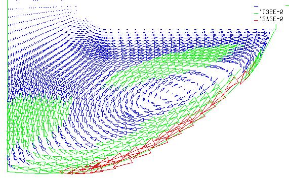
19 Fillet Lifting Lead Free Marangoni Flow TIME Solidification Stress


20 THERMAL CYCLING Reliability Modelling requirements Creep constitutive law. Lifetime model Materials Data Young s Modulus Poisons Ratio Encapsulant Solder bumps PCB CHIP Coefficient of Thermal Expansion ISSUES Microstructure changes Voids Materials data from bulk or joint tests Underfill Die Solder Cu pad Substrate
21 Thermal Cycling Flip Chip Creep Strain rate (Darveaux) [ ] n Q = A sinh( ασ ) exp( ) cr eff RT ε Lifetime Model (Coffin Manson). N f = 0.38 ( ε cr sum ) s σ ij eff Temperature Stress Creep Strain
22 Underfill Material Properties Parametric Study Models can help to identify optimal underfill Number of cycles to failure Coef Thermal Expansion (ppm) Youngs Modulus (GPa)

 Shear")

23 Modelling Microstructure effects : OOF s (NIST) Shear stress micrograph Adaptive mesh FE analysis


24 Microstructure Modelling: examples Case 1 Case 1 Case 2 Maximum creep strains are dependent on grain distributions. Case 2
25 Modelling Lead Free Materials OBJECTIVES Build 3-D Model of R geometry data supplied by National Physics Laboratory (UK) Predict stress-strain profiles and damage in PbSn solder for Different temperature cycle times Build model for Lead Free Solder (Data obtained from literature) Investigate response to different temperature cycles
26 Creep Law for solder γ cr = A sinh n ( ασ ) exp( Q RT ) Sn-Pb A=9.60E4/s, n=3.3, alpha=0.087/mpa, Q= R Sn-Ag A=9E5 (1/s) n = 5.5 a = /MPa Q = 8690R reference: R. Darveaux and K. Banerji, Ball Grid Array Technology,1995,McGraw-Hill,pp


27 Damage prediction Lifetime models only available for SnPb. No lifetime data for Lead-Free Accumulated strain energy density per thermal cycle is used as damage indicator V2 V1
28 Temperature profiles - Supplied by NPL Temperature(degrees) D time(minutes) C A B Damage Modelling Results for SnPb D t(minutes) C A B Thermal cycles: Profile A, B and C are measured oven temperature Accumulated strain energy density (Damage) Profile D is hypothetical


29 NPL Project: Damage in Solder Creep Strain Energy Density used as damage indicator. V2 V1 Symmetry Plane Effective stress when thermal load is applied. Strain energy density at the end of a thermal cycle
30 Damage in SnAg and SnPb Joints Damage D t(minutes) C B Damage(MPa) Per Cycle Solder Area A B C D SnAg SnPb Modelling Results for SnAg A V2 V1 10% More damage in SnAg V V V V
31 Conclusions Definite lack of data for lead-free solders. Key model requirements Thermal data Mechanical data All temperature dependent. Need set of experiments for creep data and lifetime relationships Effect of microstructure needs to be addressed. Link between manufacturing and reliability models required.
Thermo-Mechanical FEM Analysis of Lead Free and Lead Containing Solder for Flip Chip Applications
 Thermo-Mechanical FEM Analysis of Lead Free and Lead Containing Solder for Flip Chip Applications M. Gonzalez 1, B. Vandevelde 1, Jan Vanfleteren 2 and D. Manessis 3 1 IMEC, Kapeldreef 75, 3001, Leuven,
Effect of Underfill Entrapment on the Reliability of Flip-Chip Solder Joint
 Y. C. Chan e-mail: eeycchan@cityu.edu.hk M. O. Alam K. C. Hung H. Lu C. Bailey EPA Centre, Department of Electronic Engineering, City University of Hong Kong, Hong Kong, China; School of Computing and
Modeling the Effect of Microstructure in BGA Joints
 Intl. Journal of Microcircuits and Electronic Packaging Modeling the Effect of Microstructure in BGA Joints S. J. Holden and E. R. Wallach Department of Materials Science and Metallurgy Cambridge University
Solder joint reliability of plastic ball grid array with solder bumped flip chip
 ball grid array with solder bumped Shi-Wei Ricky Lee Department of Mechanical Engineering, The Hong Kong University of Science and, Kowloon, Hong Kong John H. Lau Express Packaging Systems, Inc., Palo
Design for Plastic Ball Grid Array Solder Joint Reliability. S.-W. R. Lee, J. H. Lau*
 Page 1 of 9 Design for Plastic Ball Grid Array Solder Joint Reliability The Authors S.-W. R. Lee, J. H. Lau* S.-W. R. Lee, Department of Mechanical Engineering, The Hong Kong University of Science and
Effect of Chip Dimension and Substrate Thickness on the Solder Joint Reliability of Plastic Ball Grid Array Packages* S.-W. Lee, J.H.
 Page 1 of 9 Effect of Chip Dimension and Substrate Thickness on the Solder Joint Reliability of Plastic Ball Grid Array Packages* The Authors S.-W. Lee, J.H. Lau** S.-W. Lee, Center for Advanced Engineering
Lead Free Surface Mount Technology. Ian Wilding BSc Senior Applications Engineer Henkel Technologies
 Lead Free Surface Mount Technology Ian Wilding BSc Senior Applications Engineer Henkel Technologies Overview of the Presentation First contact: Impact on the production operator Packaging Labelling Impact
Effects of Design, Structure and Material on Thermal-Mechanical Reliability of Large Array Wafer Level Packages
 Effects of Design, Structure and Material on Thermal-Mechanical Reliability of Large Array Wafer Level Packages Bhavesh Varia 1, Xuejun Fan 1, 2, Qiang Han 2 1 Department of Mechanical Engineering Lamar
TEMPERATURE CYCLING AND FATIGUE IN ELECTRONICS
 TEMPERATURE CYCLING AND FATIGUE IN ELECTRONICS Gilad Sharon, Ph.D. DfR Solutions Beltsville, MD, USA gsharon@dfrsolutions.com Greg Caswell DfR Solutions Liberty Hill, TX, USA gcaswell@dfrsolutions.com
Solder joint reliability of cavity-down plastic ball grid array assemblies
 cavity-down plastic ball grid array S.-W. Ricky Lee Department of Mechanical Engineering, The Hong Kong University of Science and, Kowloon, Hong Kong John H. Lau Express Packaging Systems, Inc., Palo Alto,
Lead Free Soldering Technology
 Lead Free Soldering Technology Chung-Ang University Young-Eui Shin Trend of Package Small, Light, High performance High speed, Large capacity High integrity, High density Comparison of package size 45mm
Flip Chip Bump Electromigration Reliability: A comparison of Cu Pillar, High Pb, SnAg, and SnPb Bump Structures
 Flip Chip Bump Electromigration Reliability: A comparison of Cu Pillar,,, and SnPb Bump Structures Ahmer Syed, Karthikeyan Dhandapani, Lou Nicholls, Robert Moody, CJ Berry, and Robert Darveaux Amkor Technology
Study of the Interface Microstructure of Sn-Ag-Cu Lead-Free Solders and the Effect of Solder Volume on Intermetallic Layer Formation.
 Study of the Interface Microstructure of Sn-Ag-Cu Lead-Free Solders and the Effect of Solder Volume on Intermetallic Layer Formation. B. Salam +, N. N. Ekere, D. Rajkumar Electronics Manufacturing Engineering
Characterization of Coined Solder Bumps on PCB Pads
 Characterization of Coined Solder Bumps on PCB Pads Jae-Woong Nah, Kyung W. Paik, Won-Hoe Kim*, and Ki-Rok Hur** Department of Materials Sci. & Eng., Korea Advanced Institute of Science and Technology
Parametric Design and Reliability Analysis of Wire Interconnect Technology Wafer Level Packaging
 Y. T. Lin Graduate Assistant C. T. Peng Graduate Assistant K. N. Chiang Associate Professor e-mail: Knchiang@pme.nthu.edu.tw Dept. of Power Mechanical Engineering, National Tsing Hua University, HsinChu
Welcome to SMTA Brazil Chapter Brook Sandy-Smith Dr. Ron Lasky Tim Jensen
 Welcome to SMTA Brazil Chapter 2013 Presented by Authors Ivan Castellanos Edward Briggs Brook Sandy-Smith Dr. Ron Lasky Tim Jensen Advantages / Concerns HP testing Mechanical properties New work Area ratio
System-in-Package Research within the IeMRC
 LANCASTER U N I V E R S I T Y Centre for Microsystems Engineering Faculty of Applied Sciences System-in-Package Research within the IeMRC Prof. Andrew Richardson (Lancaster University) Prof. Chris Bailey
Packaging Effect on Reliability for Cu/Low k Damascene Structures*
 Packaging Effect on Reliability for Cu/Low k Damascene Structures* Guotao Wang and Paul S. Ho Laboratory of Interconnect & Packaging, TX 78712 * Work supported by SRC through the CAIST Program TRC 2003
IMPACT OF MICROVIA-IN-PAD DESIGN ON VOID FORMATION
 IMPACT OF MICROVIA-IN-PAD DESIGN ON VOID FORMATION Frank Grano, Felix Bruno Huntsville, AL Dana Korf, Eamon O Keeffe San Jose, CA Cheryl Kelley Salem, NH Joint Paper by Sanmina-SCI Corporation EMS, GTS
Adaption to scientific and technical progress under Directive 2002/95/EC
 . Adaption to scientific and technical progress under Directive 2002/95/EC Results previous evaluation Exemption No. 15 Lead in solders to complete a viable electrical connection between semiconductor
Basic PCB Level Assembly Process Methodology for 3D Package-on-Package
 Basic PCB Level Assembly Process Methodology for 3D Package-on-Package Vern Solberg STC-Madison Madison, Wisconsin USA Abstract The motivation for developing higher density IC packaging continues to be
Adaption to scientific and technical progress under Directive 2002/95/EC
 . Adaption to scientific and technical progress under Directive 2002/95/EC Results previous evaluation Exemption No. 7 a a) Lead in high melting temperature type solders (i.e. lead-based alloys containing
Modelling Reliability of Power Electronics Modules Current Status and Future Challenges Prof Chris Bailey University of Greenwich
 Modelling Reliability of Power Electronics Modules Current Status and Future Challenges Prof Chris Bailey University of Greenwich Department of Electrical and Electronic Engineering Contents University
White Paper Quality and Reliability Challenges for Package on Package. By Craig Hillman and Randy Kong
 White Paper Quality and Reliability Challenges for Package on Package By Craig Hillman and Randy Kong Background Semiconductor technology advances have been fulfilling Moore s law for many decades. However,
Lead-Free Solder Bump Technologies for Flip-Chip Packaging Applications
 Lead-Free Solder Bump Technologies for Flip-Chip Packaging Applications Zaheed S. Karim 1 and Jim Martin 2 1 Advanced Interconnect Technology Ltd. 1901 Sunley Centre, 9 Wing Yin Street, Tsuen Wan, Hong
Selection and Application of Board Level Underfill Materials
 Selection and Application of Board Level Underfill Materials Developed by the Underfill Materials Design, Selection and Process Task Group (5-24f) of the Assembly and Joining Committee (5-20) of IPC Supersedes:
Chapter 14. Designing with FineLine BGA Packages
 Chapter 14. Designing with FineLine BGA Packages S53009-1.3 Chapter 14, Designing with FineLine BGA Packages, replaces AN 114: Designing with FineLine BGA Packages. Introduction As programmable logic devices
ROOM TEMPERATURE FAST FLOW REWORKABLE UNDERFILL FOR LGA
 As originally published in the SMTA Proceedings ROOM TEMPERATURE FAST FLOW REWORKABLE UNDERFILL FOR LGA Mary Liu, Ph.D., and Wusheng Yin, Ph.D. YINCAE Advanced Materials, LLC Albany, NY, USA wyin@yincae.com
Field Condition Reliability Assessment for SnPb and SnAgCu Solder Joints in Power Cycling Including Mini Cycles
 Field Condition Reliability Assessment for SnPb and SnAgCu Solder Joints in Power Cycling Including Mini Cycles Min Pei 1, Xuejun Fan 2 and Pardeep K. Bhatti 2 1 Georgia Tech, 801 Ferst Dr. NW, Atlanta,
Reliability of Interconnects in LED Lighting Assemblies Utilizing Metal Clad Printed Circuit Boards Stefano Sciolè BDM I.M.S.
 Reliability of Interconnects in LED Lighting Assemblies Utilizing Metal Clad Printed Circuit Boards Stefano Sciolè BDM I.M.S. Henkel Electronic Materials Agenda 1. Introduction 2. Motivation 3. Interconnect
Freescale Semiconductor Tape Ball Grid Array (TBGA) Overview
 Overview") Freescale Semiconductor Tape Ball Grid Array (TBGA) Overview Revision 0 2006 Freescale and the Freescale logo are trademarks of Freescale Semiconductor, Inc. All other product or service names are the
Freescale Semiconductor Tape Ball Grid Array (TBGA) Overview Revision 0 2006 Freescale and the Freescale logo are trademarks of Freescale Semiconductor, Inc. All other product or service names are the
Fatigue damage in microelectronic packages. H. Lu & R. Das Department of Mechanical and Industrial Engineering, Ryerson University, Toronto, Canada
 Chapter Thirteen Fatigue damage in microelectronic packages H. Lu & R. Das Department of Mechanical and Industrial Engineering, Ryerson University, Toronto, Canada Abstract This chapter aims to present
BGA Package Underfilm for Autoplacement. Jan Danvir Tom Klosowiak
 BGA Package Underfilm for Autoplacement Jan Danvir Tom Klosowiak NIST-ATP Acknowledgment Project Brief Microelectronics Manufacturing Infrastructure (October 1998) Wafer-Scale Applied Reworkable Fluxing
System Level Effects on Solder Joint Reliability
 System Level Effects on Solder Joint Reliability Maxim Serebreni 2004 2010 Outline Thermo-mechanical Fatigue of solder interconnects Shear and tensile effects on Solder Fatigue Effect of Glass Style on
New Pb-Free Solder Alloy for Demanding Applications. Presented by Karl Seelig, VP Technology, AIM
 New Pb-Free Solder Alloy for Demanding Applications Presented by Karl Seelig, VP Technology, AIM Why REL? The evolution and expansion of electronics into more harsh operating environments performing more
Lifetime Prediction and Design Tool Development for Power Electronics Modules
 Lifetime Prediction and Design Tool Development for Power Electronics Modules Dr Hua Lu and Prof. Chris Bailey University of Greenwich 30 Park Row, London SE0 9 LS IeMRC and Electronics Yorkshire Technical
TIN-BASED LEAD-FREE SOLDER BUMPS FOR FLIP-CHIP APPLICATION. S. Yaakup, H. S. Zakaria, M. A. Hashim and A. Isnin
 TIN-BASED LEAD-FREE SOLDER BUMPS FOR FLIP-CHIP APPLICATION S. Yaakup, H. S. Zakaria, M. A. Hashim and A. Isnin Advanced Materials Research Centre (AMREC), SIRIM Berhad, Lot 34, Jalan Hi-Tech 2/3, Kulim
Reliability of Lead-Free Solder Connections for Area-Array Packages
 Presented at IPC SMEMA Council APEX SM 2001 For additional information, please email marketing@amkor.com Reliability of Lead-Free Solder Connections for Area-Array Packages Ahmer Syed Amkor Technology,
Low Cycle Fatigue Testing of Ball Grid Array Solder Joints under Mixed-Mode Loading Conditions
 Tae-Sang Park Mechatronics & Manufacturing Technology Center, Corporate Technology Operations, Samsung Electronics Co., LTD, 416, Maetan-3Dong, Yeongtong-Gu, Suwon-City, Gyeonggi-Do, 443-742, Korea e-mail:
EVOLUTION OF INTERNAL STATES IN A SN-PB SOLDER JOINT DURING RE-FLOW AND THERMAL CYCLES
 EVOLUTION OF INTERNAL STATES IN A SN-PB SOLDER JOINT DURING RE-FLOW AND THERMAL CYCLES Liew Yek Ban 1, Mohd Nasir Tamin 1 and Goh Teck Joo 2 1 Faculty of Mechanical Engineering, Universiti Teknologi Malaysia,
Mechanical Behavior of Flip Chip Packages under Thermal Loading
 Mechanical Behavior of Flip Packages under Thermal Loading *Shoulung Chen 1,2, C.Z. Tsai 1,3, Nicholas Kao 1,4, Enboa Wu 1 1 Institute of Applied Mechanics, National Taiwan University 2 Electronics Research
Modelling Reliability of Power Electronics Modules Current Status, Future Challenges
 Modelling Reliability of Power Electronics Modules Current Status, Future Challenges Chris Bailey University of Greenwich, UK (c) University of Greenwich University of Greenwich Royal Observatory Computational
IPC -7095C Design and Assembly Process Implementation For BGAs
 IPC -7095C Design and Assembly Process Implementation For BGAs 1 Overview With the introduction of BGA components, things had to change: New design New assembly process New repair process New inspection
3D-WLCSP Package Technology: Processing and Reliability Characterization
 3D-WLCSP Package Technology: Processing and Reliability Characterization, Paul N. Houston, Brian Lewis, Fei Xie, Ph.D., Zhaozhi Li, Ph.D.* ENGENT Inc. * Auburn University ENGENT, Inc. 2012 1 Outline Packaging
Reflow profile study of the Sn-Ag-Cu solder
 B. Salam School of Engineering, University of Greenwich, Kent, UK C. Virseda European Fuel Cell H. Da School of Engineering, University of Greenwich, Kent, UK N.N. Ekere School of Engineering, University
White Paper 0.3mm Pitch Chip Scale Packages: Changes and Challenges
 White Paper 0.3mm Pitch Chip Scale Packages: Changes and Challenges 0.3mm Pitch Chip Scale Packages: Changes and Challenges Industry Trend The movement to 0.3mm pitch in chip scale packages (CSPs) can
Designing With High-Density BGA Packages for Altera Devices. Introduction. Overview of BGA Packages
 Designing With High-Density BGA Packages for Altera Devices December 2007, ver. 5.1 Application Note 114 Introduction As programmable logic devices (PLDs) increase in density and I/O pins, the demand for
PROCESSING AND RELIABILITY OF LOW-SILVER-ALLOYS
 PROCESSING AND RELIABILITY OF LOW-SILVER-ALLOYS Mathias Nowottnick and Andrej Novikov University of Rostock Rostock, Germany mathias.nowottnick@uni-rostock.de Joerg Trodler W.C. Heraeus Hanau, Germany
Low Cycle Thermal Fatigue of Ball Grid Array Components
 Abstract Debbie Detch ddetch@tentechllc.com William Villers wvillers@ tentechllc.com www.tentechllc.com 100 Corporate Pointe, Suite 75 Culver City, CA 9045-761 (44) 704 5 Low Cycle Thermal Fatigue of Ball
Henkel Pb-Free Soldering Technology
 Transitioning to a Pb-free Process Dr. Brian J. Toleno Americas Application Engineering Team Leader brian.toleno@us.henkel.com Henkel Technologies Marketplace - Alloy Selection Japan still a range of materials
Discrete Capacitor & Resistor Issues. Anthony Primavera Boston Scientific CRM 11/13/06
 Discrete Capacitor & Resistor Issues Anthony Primavera Boston Scientific CRM 11/13/06 Goal: Drive the Industry towards common test methods and best practices in manufacturing to reduce and or eliminate
LS720V Series. Comparison of crack progression between Sn-Cu-Ni-Ge and M773. Development of Ag-free/M773 alloy
 LS72V Series Low-Ag/Ag-free solder pastes with lower void Reduces voids by improving fluidity of flux during solder melting Reduces voids even in bottom surface electrode type components by improving solder
Bonding Technologies for 3D-Packaging
 Dresden University of Technology / Karsten Meier, Klaus-Juergen Wolter NanoZEIT seminar @ SEMICON Europa 2011 Dresden System integration by SoC or SiP solutions offer advantages regarding design efforts,
Modelling Embedded Die Systems
 Modelling Embedded Die Systems Stoyan Stoyanov and Chris Bailey Computational Mechanics and Reliability Group (CMRG) University of Greenwich, London, UK 22 September 2016 IMAPS/NMI Conference on EDT Content
EXTRA FINE PITCH FLIP CHIP ASSEMBLY PROCESS, UNDERFILL EVALUATION AND RELIABILITY
 As originally published in the SMTA Proceedings EXTRA FINE PITCH FLIP CHIP ASSEMBLY PROCESS, UNDERFILL EVALUATION AND RELIABILITY Fei Xie, Ph.D. *, Daniel F. Baldwin, Ph.D. *, Han Wu *, Swapon Bhattacharya,
Design for Flip-Chip and Chip-Size Package Technology
 Design for Flip-Chip and Chip-Size Package Technology Vern Solberg Solberg Technology Consulting Madison, Wisconsin Abstract As new generations of electronic products emerge they often surpass the capability
Available online at ScienceDirect. Procedia Engineering 79 (2014 )
") Available online at www.sciencedirect.com ScienceDirect Procedia Engineering 79 (2014 ) 333 338 37th National Conference on Theoretical and Applied Mechanics (37th NCTAM 2013) & The 1st International Conference
Available online at www.sciencedirect.com ScienceDirect Procedia Engineering 79 (2014 ) 333 338 37th National Conference on Theoretical and Applied Mechanics (37th NCTAM 2013) & The 1st International Conference
14. Designing with FineLine BGA Packages
 14. Designing with FineLine BGA Packages S51014-1.0 Chapter 14, Designing with FineLine BGA Packages, replaces AN 114: Designing with FineLine BGA Packages. Introduction As programmable logic devices (PLDs)
IMPACT OF LEAD-FREE COMPONENTS AND TECHNOLOGY SCALING FOR HIGH RELIABILITY APPLICATIONS
 IMPACT OF LEAD-FREE COMPONENTS AND TECHNOLOGY SCALING FOR HIGH RELIABILITY APPLICATIONS Chris Bailey, Ph.D. University of Greenwich London, United Kingdom c.bailey@gre.ac.uk ABSTRACT Semiconductor technology
Bridging Supply Chain Gap for Exempt High-Reliability OEM s
 Bridging Supply Chain Gap for Exempt High-Reliability OEM s Hal Rotchadl hrotchadl@premiers2.com www.premiers2.com Premier Semiconductor Services Tempe, AZ RoHS exempt high reliability OEMs breathed a
S3X58-M ICT Compatible Lead Free Solder Paste. Product Information. Koki no-clean LEAD FREE solder paste. Contents.
 Koki no-clean LEAD FREE solder paste www.ko-ki.co.jp #53002 Revised on Mar. 3, 2015 ICT Compatible Lead Free Solder Paste Product Information Conventional Product Picture of ICT Checker Probe The product
Silicon Wafer Processing PAKAGING AND TEST
 Silicon Wafer Processing PAKAGING AND TEST Parametrical test using test structures regularly distributed in the wafer Wafer die test marking defective dies dies separation die fixing (not marked as defective)
HOW THE MOLD COMPOUND THERMAL EXPANSION OVERRULES THE SOLDER COMPOSITION CHOICE IN BOARD LEVEL RELIABILITY PERFORMANCE
 HOW THE MOLD COMPOUND THERMAL EXPANSION OVERRULES THE SOLDER COMPOSITION CHOICE IN BOARD LEVEL RELIABILITY PERFORMANCE AUTHORS: B. VANDEVELDE, L. DEGRENDELE, M. CAUWE, B. ALLAERT, R. LAUWAERT, G. WILLEMS
Manufacturing and Reliability Challenges With QFN
 Manufacturing and Reliability Challenges With QFN Dr. Craig Hillman and Cheryl Tulkoff DfR Solutions SMTA DC Chapter Ashburn, VA February 25, 2009 QFN as a Next Generation Technology What is Next Generation
A Proposed Mechanism and Remedy for Ball-in-Socket and Foot-in-Mud Soldering Defects on Ball Grid Array and Quad Flat Pack Components
 A Proposed Mechanism and Remedy for Ball-in-Socket and Foot-in-Mud Soldering Defects on Ball Grid Array and Quad Flat Pack Components Brian Smith Kester Des Plaines, IL Abstract A common source of defects
High-Reliability Lead-Free Solder Paste M705-GRN360-K-V. Senju Metal Industry Co.,Ltd. Senju Manufacturing (Europe) Ltd.
 Ltd.") Senju Metal Industry Co., Ltd. High-Reliability Lead-Free Solder Paste Manufacturer Senju Metal Industry Co.,Ltd. 23 Senju Hashido-cho, Adachi-Ku, Tokyo, Japan Phone: +81-33888-5156 Fax: +81-33870-3032
Senju Metal Industry Co., Ltd. High-Reliability Lead-Free Solder Paste Manufacturer Senju Metal Industry Co.,Ltd. 23 Senju Hashido-cho, Adachi-Ku, Tokyo, Japan Phone: +81-33888-5156 Fax: +81-33870-3032
TECHNOLOGIES FOR APPLYING FLUIDS IN SEMICONDUCTOR PACKAGING
 TECHNOLOGIES FOR APPLYING FLUIDS IN SEMICONDUCTOR PACKAGING Alec J. Babiarz Asymtek Carlsbad, CA, USA ajbabiarz@asymtek.com ABSTRACT Jetting fluids in semiconductor packaging and assembly has become an
Simulations and Characterizations for Stress Reduction Designs in Wafer Level Chip Scale Packages
 Simulations and Characterizations for Stress Reduction Designs in Wafer Level Chip Scale Packages by Ming-Che Hsieh STATS ChipPAC Taiwan Co. Ltd. Copyright 2013. Reprinted from 2013 International Microsystems,
EPOXY FLUX MATERIAL AND PROCESS FOR ENHANCING ELECTRICAL INTERCONNECTIONS
 As originally published in the SMTA Proceedings. EPOXY FLUX MATERIAL AND PROCESS FOR ENHANCING ELECTRICAL INTERCONNECTIONS Neil Poole, Ph.D., Elvira Vasquez, and Brian J. Toleno, Ph.D. Henkel Electronic
2. Description of materials and equipment for which the exemption is required
 Application for granting a new RoHS exemption: Leaded solder utilized in stacked, area array electronics packaging within ionizing radiation detectors including CT and X-ray Name and address of applicant
Effect of Encapsulation Materials on Tensile Stress during Thermo-Mechanical Cycling of Pb-Free Solder Joints
 Effect of Encapsulation Materials on Tensile Stress during Thermo-Mechanical Cycling of Pb-Free Solder Joints Maxim Serebreni, Dr. Nathan Blattau, Dr. Gilad Sharon, Dr. Craig Hillman DfR Solutions Beltsville,
Material Selection and Parameter Optimization for Reliable TMV Pop Assembly
 Selection and Parameter Optimization for Reliable TMV Pop Assembly Brian Roggeman, David Vicari Universal Instruments Corp. Binghamton, NY, USA Roggeman@uic.com Martin Anselm, Ph.D. - S09_02.doc Lee Smith,
Best Practice Guide for Thermocycling and Reliability Assessment of Solder Joints
 Best Practice Guide for Thermocycling and Reliability Assessment of Solder Joints Miloš Dušek and Christopher Hunt July 2000 July 2000 Best Practice Guide for Thermocycling and Reliability Assessment of
Koki no-clean LEAD FREE solder paste. High-reliability Low Ag Lead Free Solder Paste
 www.ko-ki.co.jp #514- Revised on Feb.4, 214 Koki no-clean LEAD FREE solder paste High-reliability Low Ag Lead Free Solder Paste S1XBIG58-M5-4 Product information S1XBIG SAC35 After -4/125ºC, 1 cycles This
Advanced Analytical Techniques for Semiconductor Assembly Materials and Processes. Jason Chou and Sze Pei Lim Indium Corporation
 Advanced Analytical Techniques for Semiconductor Assembly Materials and Processes Jason Chou and Sze Pei Lim Indium Corporation Agenda Company introduction Semiconductor assembly roadmap challenges Fine
Becoming Lead Free. Automotive Electronics. Antonio Aires Soldering Technical Specialist Visteon Corporation - Palmela Plant
 Automotive Electronics Becoming Lead Free Antonio Aires Soldering Technical Specialist Visteon Corporation - Palmela Plant 1 Agenda 1. Leadfree Electronics Drivers 2. Requirements 3. Areas of Impact 4.
Journal of Science and Technology The Investigation of Die Back Edge Cracking in Flip Chip Ceramic Ball Grid Array Package (FC-CBGA)
") The Investigation of Die Back Edge Cracking in Flip Chip Ceramic Ball Grid Array Package (FC-CBGA) Zainudin Kornain a, Azman Jalar a, Rozaidi Rasid b, a Institute of Microengineering and Nanoelectronics
The Investigation of Die Back Edge Cracking in Flip Chip Ceramic Ball Grid Array Package (FC-CBGA) Zainudin Kornain a, Azman Jalar a, Rozaidi Rasid b, a Institute of Microengineering and Nanoelectronics
Chapter 4. Numerical analysis using finite element simulation
 Chapter 4. Numerical analysis using finite element simulation 4.1 Introduction to numerical analysis Humans divide almost everything into components for the purpose of gaining a better understanding: The
Effects of Bi Content on Mechanical Properties and Bump Interconnection Reliability of Sn-Ag Solder Alloys
 Effects of Bi Content on Mechanical Properties and Bump Interconnection Reliability of Sn-Ag Solder Kazuki Tateyama, Hiroshi Ubukata*, Yoji Yamaoka*, Kuniaki Takahashi*, Hiroshi Yamada** and Masayuki Saito
S/C Packaging Assembly Challenges Using Organic Substrate Technology
 S/C Packaging Assembly Challenges Using Organic Substrate Technology Presented by Bernd Appelt ASE Group Nov. 17, 2009 Overview The Packaging Challenge Chip Substrate Interactions Stiffeners for FC-BGA
Lead Free Solder for Flip Chip
 Lead Free Solder for Flip Chip Zhenwei Hou & R. Wayne Johnson Laboratory for Electronics Assembly & Packaging Auburn University 162 Broun Hall, ECE Dept. Auburn, AL 36489 USA 334-844-1880 johnson@eng.auburn.edu
Reliability of Pb-Free Solder Alloys in Demanding BGA and CSP Applications
 Reliability of Pb-Free Solder Alloys in Demanding BGA and CSP Applications Ranjit Pandher and Robert Healey Cookson Electronics 109 Corporate Blvd. South Plainfield, NJ 07080, USA Email: rpandher@cooksonelectronics.com
WF6317. A superactive low-volatile/high heat-resistant water-soluble flux for ball soldering
 WF637 A superactive low-volatile/high heat-resistant water-soluble flux for ball soldering Low viscosity and high tacking power stabilize ball holding force and ensures excellent solder wettability Easy
S3X58-G801. High Performance Low Voiding LF Solder Paste. Product Information. Koki no-clean LEAD FREE solder paste.
 www.ko-ki.co.jp #55001-3 First issue: Jan.13, 2017 Revised: Jun. 28, 2017 Koki no-clean LEAD FREE solder paste High Performance Low Voiding LF Solder Paste S3X58-G801 Product Information 0603R 0603R Disclaimer
Unique Failure Modes from use of Sn-Pb and Lead-Free (mixed metallurgies) in PCB Assembly: CASE STUDY
 in PCB Assembly: CASE STUDY") Unique Failure Modes from use of Sn-Pb and Lead-Free (mixed metallurgies) in PCB Assembly: CASE STUDY Frank Toth, and Gary F. Shade; Intel Corporation, Hillsboro, OR, USA {francis.toth.jr@intel.com, (503)-696-1546}
Unique Failure Modes from use of Sn-Pb and Lead-Free (mixed metallurgies) in PCB Assembly: CASE STUDY Frank Toth, and Gary F. Shade; Intel Corporation, Hillsboro, OR, USA {francis.toth.jr@intel.com, (503)-696-1546}
LEAD-BASED solders have been used to provide electrical
 38 IEEE TRANSACTIONS ON ADVANCED PACKAGING, VOL. 30, NO. 1, FEBRUARY 2007 Effects of Phase Change of Pb-Free Flip-Chip Solders During Board-Level Interconnect Reflow Soonwan Chung, Zhenming Tang, and Seungbae
Manufacturing of electronic equipment
 Manufacturing of electronic equipment 13.10.2016 Objective: To give a generic understanding on the manufacturing methods and 2 nd level interconnection materials of electronic equipments Literature: K.
Solder paste reflow modeling for flip chip assembly
 Loughborough University Institutional Repository Solder paste reflow modeling for flip chip assembly This item was submitted to Loughborough University's Institutional Repository by the/an author. Citation:
Reliability of RoHS-Compliant 2D and 3D 1С Interconnects
 Reliability of RoHS-Compliant 2D and 3D 1С Interconnects John H. Lau, Ph.D. New York Chicago San Francisco Lisbon London Madrid Mexico City Milan New Delhi San Juan Seoul Singapore Sydney Toronto Foreword
INEMI Packaging Substrate Workshop, Toyama, Japan, 2014 Challenges of Organic Substrates from EMS Perspective Weifeng Liu, Ph. D.
 INEMI Packaging Substrate Workshop, Toyama, Japan, 2014 Challenges of Organic Substrates from EMS Perspective Weifeng Liu, Ph. D. Date (4/10/2014) AEG - WW Microelectronics and Packaging OUTLINE Overview
ALPHA OM-5100 FINE PITCH SOLDER PASTE
 SM 797-7 ALPHA OM-5100 FINE PITCH SOLDER PASTE DESCRIPTION Cookson Electronics Assembly Material s ALPHA OM-5100, is a low residue, no-clean solder paste designed to maximize SMT line yields. The flux
Composition/wt% Bal SA2 (SABI) Bal SA3 (SABI + Cu) Bal
 Bal SA3 (SABI + Cu) Bal") Improving Thermal Cycle and Mechanical Drop Impact Resistance of a Lead-free Tin-Silver-Bismuth-Indium Solder Alloy with Minor Doping of Copper Additive Takehiro Wada 1, Seiji Tsuchiya 1, Shantanu Joshi
Improving Thermal Cycle and Mechanical Drop Impact Resistance of a Lead-free Tin-Silver-Bismuth-Indium Solder Alloy with Minor Doping of Copper Additive Takehiro Wada 1, Seiji Tsuchiya 1, Shantanu Joshi
Forward and Backward Soldering Compatibility
 Forward and Backward Soldering Compatibility You are connected to our live presentation delivered via the internet. The webinar will begin shortly. NEW 1 Attendee Quick Reference You can ask questions
NUMERICAL MODELING OF CYCLIC STRESS-STRAIN BEHAVIOR OF Sn-Pb SOLDER JOINT DURING THERMAL FATIGUE
 NUMERICAL MODELING OF CYCLIC STRESS-STRAIN BEHAVIOR OF Sn-Pb SOLDER JOINT DURING THERMAL FATIGUE M.N. Tamin and Y.B. Liew Department of Applied Mechanics Faculty of Mechanical Engineering 81310 UTM Skudai,
Effects of Solder Reflow on the Reliability of Flip-Chip on Flex Interconnections Using Anisotropic Conductive Adhesives
 254 IEEE TRANSACTIONS ON ELECTRONICS PACKAGING MANUFACTURING, VOL. 27, NO. 4, OCTOBER 2004 Effects of Solder Reflow on the Reliability of Flip-Chip on Flex Interconnections Using Anisotropic Conductive
JOINT INDUSTRY STANDARD
 JOINT INDUSTRY STANDARD AUGUST 1999 Semiconductor Design Standard for Flip Chip Applications ASSOCIATION CONNECTING ELECTRONICS INDUSTRIES Semiconductor Design Standard for Flip Chip Applications About
Low-Silver BGA Assembly Phase II Reliability Assessment Fifth Report: Preliminary Thermal Cycling Results
 Low-Silver BGA Assembly Phase II Reliability Assessment Fifth Report: Preliminary Thermal Cycling Results Gregory Henshall 1 Michael Fehrenbach 2 Hewlett-Packard Co. 1 Palo Alto, CA USA 2 Houston, TX USA
room and cold readouts were performed every 250 cycles. Failure data and Weibull plots were generated. Typically, the test vehicles were subjected to
 SOLDER JOINT RELIABILITY ASSESMENT OF Sn-Ag-Cu BGA COMPONENTS ATTACHED WITH EUTECTIC Pb-Sn SOLDER Fay Hua 1, Raiyo Aspandiar 2, Cameron Anderson 3, Greg Clemons 3, Chee-key Chung 4, Mustapha Faizul 4 Intel
Sherlock 4.0 and Printed Circuit Boards
 Sherlock 4.0 and Printed Circuit Boards DfR Solutions January 22, 2015 Presented by: Dr. Nathan Blattau Senior Vice President 9000 Virginia Manor Rd Ste 290, Beltsville MD 20705 301-474-0607 www.dfrsolutions.com