9:00 Intro to pyrite, collaboration Matt Law 9:20 Phase Field Crystal (PFC) modeling John Lowengrub 9:40 CVD thin film growth Nick Berry 9:55 XPS
|
|
|
- Darren Bennett
- 6 years ago
- Views:
Transcription


1 Pyrite FeS 2 Kickoff Meeting August 3, 2010
2 Meeting schedule 9:00 Intro to pyrite, collaboration Matt Law 9:20 Phase Field Crystal (PFC) modeling John Lowengrub 9:40 CVD thin film growth Nick Berry 9:55 XPS analysis of pyrite films Ming Cheng 10:10 Colloidal pyrite nanocrystals and films James Puthussery 10:25 Colloidal & molecular approaches Sean Seefeld 10:40 New ligands / Molecular approaches Amanda Weber 10:55 12:00 Discussion and planning 2
3 Earth-abundant materials for photovoltaics (PV) The dominant thin film technologies (CdTe, CuIn x Ga 1-x Se 2 ) are based on rare, toxic 3elements.


, versus crystalline")


4 First Solar CdTe thin film company Largest thin film manufacturer 1.25 GW/yr manufacturing capacity in 2010, projected 1.8 GW/yr in 2012 $0.85/watt module manufacturing cost (3Q 2009), versus crystalline silicon which is closer to $3/watt First Solar s average module efficiency is 11% (3Q 2009) Best CdTe cell efficiency is 16.5% (NREL) Module cost < 50% total installed cost 40-MW installation in Waldpolenz, Germany Thin film array at Dimbach, Germany. 1.3 MW using First Solar Thin Film modules Scalable to TWs? 4
5 Will tellurium limit scalability of CdTe PV? U.S. Geological Survey, Mineral Commodity Summaries, January tons Te produced in GW CdTe PV uses ~90 tons Te 1 TW CdTe would require entire worldwide reserve base More Te will have to be found/mined economically 5


6 Iron Pyrite (FeS 2 ) Fool s gold Crystal structure Electronic structure suitable bandgap (0.95 ev) very strong light absorption adequate diffusion lengths extremely cheap infinitely abundant (most abundant sulfide in crust) Space group Pa3 Pyrite tops a short list of thin film materials capable of scaling to multiple TWs without resource limitations 6
7 Basic properties 7
8 Optical absorptivity 8
9 Previous work Helmut Tributsch (Hahn-Meitner Institüt) pioneered pyrite for PV starting in
10 Pyrite suffers from a low voltage Pyrite tends to be sulfur deficient, and sulfur defects create states in the bandgap, limiting the voltage Performance: 40 ma cm -2, ~0.2 V, 3.3% Passivating bulk/surface defects is the key 10 to boosting cell efficiency
11 Fe-S phase diagram 11
12 Common Fe-S phases 12
13 Science Summary Pyrite is extremely promising as a scalable PV material. It deserves another look, using modern techniques. The main limitation on the efficiency of pyrite cells is their low open-circuit voltage. The low voltage is probably caused by iron-derived gap states. The most promising way to improve the pyrite photovoltage is to passivate under-coordinated iron ions, especially at the crystal surface. 13
14 Funding: NSF s SOLAR Program Synopsis The purpose of the CHE DMR DMS Solar Energy Initiative is to support interdisciplinary efforts by groups of researchers to address the scientific challenges of highly efficient harvesting, conversion, and storage of solar energy. Groups must include three or more co Principal Investigators of whom one must be a researcher in chemistry, a second in materials, and a third in mathematical sciences in areas supported by the Divisions of Chemistry, Materials Research, and Mathematical Sciences, respectively. The intent is to encourage new collaborations in which the mathematical sciences are linked in a synergistic way with the chemical and materials sciences to develop novel, potentially transformative approaches in an area of much activity but largely incremental advances. Successful proposals will offer potentially transformative projects, new concepts, and interdisciplinary education through research involvement based on the integrated expertise and synergy from the three disciplinary communities. NSF s emphasis is the math effort: use emerging techniques in math to help mat. sci. and chemistry solve solar problems 14
15 SOLAR rd year of the SOLAR program 109 pre-proposals; p p 30 full proposals; p 9 funded Our proposal was ranked #1 We benefitted by not being an organic bulk heterojunction proposal 15
16 Collaboration overview Objective: Combine PFC and DFT modeling with pyrite growth and surface characterization to 1) )grow device-quality pyrite thin films by 2 methods 2) triple the pyrite photovoltage via passivation Law, Hemminger, Lowengrub, and Wu groups. 3 years, starting 9/1/10. Project is renewable. Funding for 5 students & postdocs. -2 synthesis/characterization (Law) - 1 surface characterization (Hemminger) - 2 modeling (Lowengrub & Wu) 16
17 Collaboration activities Model Grow Characterize WU 17
18 Modeling objectives Angstrom-to-micron capabilities PFC Ideally, show how to grow large grain, stoichiometric pyrite thin films. DFT Ideally, show how to passivate bulk/surface states to boost voltage. More realistically, help to: control gas-phase pyrite nucleation understand crystal growth predict crystal phase identify conditions for sintering understand SS diffusion improve adhesion to substrate eliminate voids minimize sulfur deficiency identify conditions for epitaxy More realistically, help to: identify origin of gap states calculate binding energies/geometries calculate formation energies vet promising surface treatments interpret/predict XPS results interpret/predict STS results simulate smulate FTIR data discriminate bulk/surface effects understand doping 18
19 Technical challenges 1. Develop and validate a PFC model for FCC pyrite 2. Develop a DFT model of pyrite (bulk & surface) With input from the models, 3. Produce high-quality pyrite films from pyrite nanocrystal paint. 4. Make high-quality pyrite films by CVD. 5. Grow epitaxial layers on silicon as model systems. 6. Develop surface passivation treatments that increase the pyrite photovoltage > 500 mv. 7. Establish causation between passivation and enhanced electronic performance. Maximize robustness of passivation. 8. By the end of the project, fabricate prototype pyrite p-n heterojunction solar cells with improved voltage and conversion efficiency. 19
20 Surface passivation strategies Moderate-temperature temperature annealing in S 2, H 2 S, and H 2 atmospheres. Coordination of surface iron with strongly-bound organic and inorganic ligands. Testing with XPS, STS, and photovoltage measurements 20
21 Project schedule Year 1: Construct PFC and DFT models and use to optimize film microstructure tune passivation treatments interpret XPS/UPS/STS data Year 2: Continuation Year 3: Be producing high-quality pyrite via both synthetic approaches. Establish the connection between microstructure, gap states, and photovoltage. By the end, make record-performance devices. 21
22 End game 22
23 Meeting schedule 9:00 Intro to pyrite, collaboration Matt Law 9:20 Phase Field Crystal (PFC) modeling John Lowengrub 9:40 CVD thin film growth Nick Berry 9:55 XPS analysis of pyrite films Ming Cheng 10:10 Colloidal pyrite nanocrystals and films James Puthussery 10:25 Colloidal & molecular approaches Sean Seefeld 10:40 New ligands / Molecular approaches Amanda Weber 10:55 12:00 Discussion and planning 23
24 24
25 25
 cubic, E g = 0.")
 diamagnetic semiconductor Greigite (Fe 3 S 4 ) cubic, E g = 0.")
 diamagnetic or ferromagnetic semiconductor Troilite (FeS) hexagonal, E g = 0.")
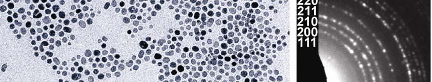
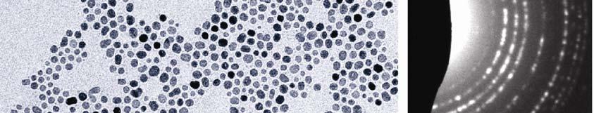
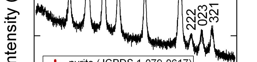
26 Synthesizing pyrite NCs is a challenge multiple Fe-S phases difficult to crystallize tends to aggregate Early results: aggregates Iron sulfide phases Pyrite (FeS 2 ) cubic, E g = 0.95 ev (indirect) Van Vleck paramagnetic semiconductor Marcasite (FeS 2 ) orthorhombic, h E g = ev V(indirect) diamagnetic semiconductor Greigite (Fe 3 S 4 ) cubic, E g = 0.4 ev, ferrimagnetic Pyrrhotite hexagonal or monoclinic, E g eV (Fe 1-x S, with x 0.2) diamagnetic or ferromagnetic semiconductor Troilite (FeS) hexagonal, E g = 0.04 ev, antiferromagnetic semiconductor 26
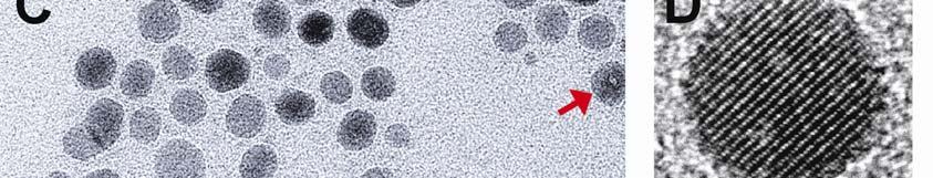
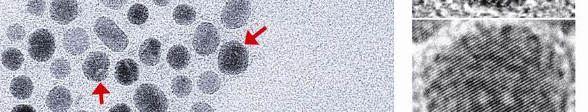
27 Pyrite nanocrystal inks 27


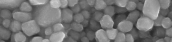
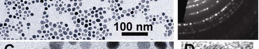
28 Polycrystalline pyrite thin films Sintering the NC films in S 2 gas gives polycrystalline pyrite 500 C 100 nm 100 nm film optimization optmzaton characterization surface passivation devices 28
The next thin-film PV technology we will discuss today is based on CIGS.
 ET3034TUx - 5.3 - CIGS PV Technology The next thin-film PV technology we will discuss today is based on CIGS. CIGS stands for copper indium gallium selenide sulfide. The typical CIGS alloys are heterogeneous
8. Summary and Outlook
 8. Summary and Outlook This thesis deals with the synthesis and evaluation of all-nitrogen coordinated complexes of the rare earths such ad Gd, Er, and Y bearing the amidinate and guanidinate class of
A Critical Review of Pyrite as a Photovoltaic Material
 A Critical Review of Pyrite as a Photovoltaic Material Divija Pandel* and Satender Dehiya** *PhD. (The Department of Metallurgical and Materials Engg.), MNIT Jaipur **M.Tech (The Department of Metallurgical
13.4 Chalcogenide solar cells Chalcopyrite solar cells
 13. Thin-Film Solar Cells 201 Figure 13.19: The crystal structure of copper indium diselenide, a typical chalcopyrite. The colors indicate copper (red), selenium (yellow) and indium (blue). For copper
An advantage of thin-film silicon solar cells is that they can be deposited on glass substrates and flexible substrates.
 ET3034TUx - 5.2.1 - Thin film silicon PV technology 1 Last week we have discussed the dominant PV technology in the current market, the PV technology based on c-si wafers. Now we will discuss a different
Why does pyrite have a low photovoltage?
 Why does pyrite have a low photovoltage? August 25, 2011 Hypothesis I: metallic phase impurities Pyrite always contains metallic FeS-type phase impurities, which somehow reduce the photovoltage Evidence
MATERIALS FOR SOLAR ENERGY: SOLAR CELLS
 MATERIALS FOR SOLAR ENERGY: SOLAR CELLS ROBERTO MENDONÇA FARIA PRESIDENT OF Brazil-MRS (SBPMat) The concentration of CO 2 in Earth s atmosphere (2011) is approximately 392 ppm (parts per million) by volume,
Materials Availability for TW Scale Photovoltaics
 Materials Availability for TW Scale Photovoltaics Eray S. Aydil University of Minnesota Department of Chemical Engineering & Materials Science aydil@umn.edu Survey of audience a) Current thin film technologies,
The Potential of Photovoltaics
 The Potential of Photovoltaics AIMCAL 2008 2008 Fall Conference Vacuum Web Coating Brent P. Nelson October 22, 2008 NREL is a national laboratory of the U.S. Department of Energy Office of Energy Efficiency
Selenium and Tellurium. G&E Ch. 16 and Supplements
 Selenium and Tellurium G&E Ch. 16 and Supplements Batteries vs. Electrolytic Cells An electrochemical cell that releases energy is called a galvanic cell (battery, power generation, ΔG
SOLAR ENERGY. Approximately 120,000 TW of solar energy strikes the earth s surface, capturing only a fraction could supply all of our energy needs.
 SOLAR ENERGY Approximately 120,000 TW of solar energy strikes the earth s surface, capturing only a fraction could supply all of our energy needs. What is Photovoltaics? Photovoltaics is a high-technology
Micron-Resolution Photocurrent of CdTe Solar Cells Using Multiple Wavelengths
 Mat. Res. Soc. Symp. Proc. Vol. 668 2001 Materials Research Society Micron-Resolution Photocurrent of CdTe Solar Cells Using Multiple Wavelengths Jason F. Hiltner 1 and James R. Sites Department of Physics,
PHYSICSOF SOLARCELLS. Jenny Nelson. Imperial College, UK. Imperial College Press ICP
 im- PHYSICSOF SOLARCELLS Jenny Nelson Imperial College, UK ICP Imperial College Press Contents Preface v Chapter 1 Introduction 1 1.1. Photons In, Electrons Out: The Photovoltaic Effect 1 1.2. Brief History
Advanced Analytical Chemistry Lecture 9. Chem 4631
 Advanced Analytical Chemistry Lecture 9 Chem 4631 Solar Cell Research Solar Cell Research Solar Cell Research Solar Cell Research Thin film technologies Candidates for thin-film solar cells: Crystalline
light to electricity in p-n junctions
 (-) (+) light e - Conducting back contact h + thin conducting transparent film n p light to electricity in p-n junctions + J - V + Dark Current - Photo Current Typical plots of current vs. applied potential
Basics of Solar Photovoltaics. Photovoltaics (PV) Lecture-21
 Lecture-21") Lecture-21 Basics of Solar Photovoltaics Photovoltaics (PV) Photovoltaics (PV) comprise the technology to convert sunlight directly into electricity. The term photo means light and voltaic, electricity.
Lecture-21 Basics of Solar Photovoltaics Photovoltaics (PV) Photovoltaics (PV) comprise the technology to convert sunlight directly into electricity. The term photo means light and voltaic, electricity.
Thin Film Solar Cells Fabrication, Characterization and Applications
 Thin Film Solar Cells Fabrication, Characterization and Applications Edited by Jef Poortmans and Vladimir Arkhipov IMEC, Leuven, Belgium John Wiley & Sons, Ltd Contents Series Preface Preface xiii xv 1
Review of Photovoltaic Solar Cells. Op5cs for Energy Course 11/5/13 Liz Lund
 Review of Photovoltaic Solar Cells Op5cs for Energy Course 11/5/13 Liz Lund Outline Solar electricity produc5on How Photovoltaics (PV) work Types of PV Emerging technologies Solar Electricity Produc5on
PROMISING THIN FILMS MATERIALS FOR PHOTOVOLTAICS
 PROMISING THIN FILMS MATERIALS FOR PHOTOVOLTAICS Emmanuelle ROUVIERE CEA Grenoble (France) emmanuelle.rouviere@cea.fr Outline Introduction Photovoltaic technologies and market Applications Promising Thin
Electricity from the Sun (photovoltaics)
") Electricity from the Sun (photovoltaics) 0.4 TW US Electricity Consumption 100 100 square kilometers of solar cells could produce all the electricity for the US. But they are still too costly. The required
Electricity from the Sun (photovoltaics) 0.4 TW US Electricity Consumption 100 100 square kilometers of solar cells could produce all the electricity for the US. But they are still too costly. The required
ET3034TUx High efficiency concepts of c- Si wafer based solar cells
 ET3034TUx - 4.4 - High efficiency concepts of c- Si wafer based solar cells In the previous block we have discussed various technological aspects on crystalline silicon wafer based PV technology. In this
Material Needs for Thin-Film and Concentrator Photovoltaic Modules
 Material Needs for Thin-Film and Concentrator Photovoltaic Modules NREL Sarah Kurtz CDMA Conference: Opportunities for Chemicals and Materials in Wind and Solar Energy December 4, 2009 Philadelphia, PA
Solar Cells Fabrication Technologies
 Solar Cells Fabrication Technologies Crystalline Si Cell Technologies Amorphous Si Cell Technologies Thin Film Cell Technologies For a comprehensive tutorial on solar cells in general, see www.udel.edu/igert/pvcdrom
Solar Photovoltaic Technologies: Past, Present and Future
 Solar Photovoltaic Technologies: Past, Present and Future Xihua Wang, Ph.D., P.Eng. Assistant Professor of Electrical & Computer Engineering University of Alberta April 18, 2018 Outline History of photovoltaic
Efficiency Enhancement of Bulk-Heterojunction
 Efficiency Enhancement of Bulk-Heterojunction Hybrid Solar Cells Michael Krüger, Yunfei Zhou, Michael Eck Freiburg Materials Research Centre (FMF), University of Freiburg, Germany Institute for Microsystems
Materials Science and Engineering: An Introduction
 Materials Science and Engineering: An Introduction Callister, William D. ISBN-13: 9780470419977 Table of Contents List of Symbols. 1 Introduction. 1.1 Historical Perspective. 1.2 Materials Science and
Thin film solar cells
 Thin film solar cells pn junction: a:si cells heterojunction cells: CIGS-based CdTe-based 1 Amorphous Si large concentration of defects N T >10 16 cm -3 ( dangling bonds D +, D -, D o ) passivation of
Photovoltaic Systems Engineering
 Photovoltaic Systems Engineering Ali Karimpour Associate Professor Ferdowsi University of Mashhad Reference for this lecture Mrs. Golmakanion Thesis Feb 2010 Ferdowsi University of Mashhad lecture 2 Lecture
ELECTRICAL PROPERTIES OF CDS THIN FILMS SPIN COATED ON CONDUCTIVE GLASS SUBSTRATES
 UDC: 538.9 Condensed matter Physics, Solid state Physics, Experimental Condensed matter Physics ELECTRICAL PROPERTIES OF CDS THIN FILMS SPIN COATED ON CONDUCTIVE GLASS SUBSTRATES P. Samarasekara and P.A.S.
Amorphous silicon / crystalline silicon heterojunction solar cell
 Workshop on "Physics for Renewable Energy" October 17-29, 2005 301/1679-9 "Amorphous Silicon / Cyrstalline Silicon Heterojunction Solar Cell" E. Centurioni CNR/IMM AREA Science Park - Bologna Italy Amorphous
Solar Cells and Photosensors.
 Designing Photonic Crystals in Strongly Absorbing Material for Applications in Solar Cells and Photosensors. Minda Wagenmaker 1, Ebuka S. Arinze 2, Botong Qiu 2, Susanna M. Thon 2 1 Mechanical Engineering
Summary and Scope for further study
 Chapter 6 Summary and Scope for further study 6.1 Summary of the present study Transparent electronics is an emerging science and technology field concentrated on fabricating invisible electronic circuits
AMORPHOUS SILICON DIOXIDE LAYER FOR HIGH EFFICIENCY CRYSTALLINE SOLAR CELLS
 International Journal of Nanotechnology and Application (IJNA) ISSN(P): 2277-4777; ISSN(E): 2278-9391 Vol. 6, Issue 5, Dec 2016, 1-6 TJPRC Pvt. Ltd. AMORPHOUS SILICON DIOXIDE LAYER FOR HIGH EFFICIENCY
Roughly 4.6 billion years ago... Let there be light
 The Past Roughly 4.6 billion years ago... Let there be light 1839 Edmund Becquerel discovers the photovoltaic effect. 1860-1881 Auguste Mouchout was the first man to patent a design for a motor running
Laser-Crystallised Thin-Film Polycrystalline Silicon Solar Cells. Jonathon Dore SPREE Research Seminar - 27th June, 2013
 Laser-Crystallised Thin-Film Polycrystalline Silicon Solar Cells Jonathon Dore SPREE Research Seminar - 27th June, 2013 Contents Introduction motivation for thin-film Thin-film PV technologies Diode laser
Plasmonic Photovoltaics
 Plasmonic Photovoltaics Investigators Harry A. Atwater, Howard Hughes Professor and Professor of Applied Physics and Materials Science, California Institute of Technology Krista Langeland, Ph.D. student,
Performance predictions for monolithic, thin-film CdTe/Ge tandem solar cells
 Performance predictions for monolithic, thin-film CdTe/Ge tandem solar cells D.L. Pulfrey*, J. Dell, and L. Faraone School of Electrical, Electronic and Computer Engineering, M018 University of Western
OPTIMIZATION OF ZINC SULFIDE (ZnS) ELECTRON AFFINITY IN COPPER INDIUM SULFIDE (CIS) BASED PHOTOVOLTAIC CELL
 ELECTRON AFFINITY IN COPPER INDIUM SULFIDE (CIS) BASED PHOTOVOLTAIC CELL") Chalcogenide Letters Vol. 10, No. 6, June 2013, p. 189-195 OPTIMIZATION OF ZINC SULFIDE (ZnS) ELECTRON AFFINITY IN COPPER INDIUM SULFIDE (CIS) BASED PHOTOVOLTAIC CELL HADIBAH RAMLI a*, SHARUL KAMAL ABDUL
Chalcogenide Letters Vol. 10, No. 6, June 2013, p. 189-195 OPTIMIZATION OF ZINC SULFIDE (ZnS) ELECTRON AFFINITY IN COPPER INDIUM SULFIDE (CIS) BASED PHOTOVOLTAIC CELL HADIBAH RAMLI a*, SHARUL KAMAL ABDUL
Polycrystalline CdS/CdTe solar cells
 Polycrystalline CdS/CdTe solar cells Al Compaan Distinguished University Professor of Physics, Emeritus (Lecture for Heben/Ellingson solar cells class) March 3, 2011 1 Absorption spectra of various semiconductors
Gerhard Rauter, COO. Q-CELLS SE Leading edge photovoltaic technologies for Europe
 Gerhard Rauter, COO Q-CELLS SE Leading edge photovoltaic technologies for Europe Q-CELLS SE Foundation: November 1999 Core business: Si-Solar Cells Start of production: 2001 Production (2007): 389 MW Number
Nucleation and growth of nanostructures and films. Seongshik (Sean) Oh
 Oh") Nucleation and growth of nanostructures and films Seongshik (Sean) Oh Outline Introduction and Overview 1. Thermodynamics and Kinetics of thin film growth 2. Defects in films 3. Amorphous, Polycrystalline
Nucleation and growth of nanostructures and films Seongshik (Sean) Oh Outline Introduction and Overview 1. Thermodynamics and Kinetics of thin film growth 2. Defects in films 3. Amorphous, Polycrystalline
Crystalline Silicon Solar Cells Future Directions. Stuart Bowden BAPVC January Stuart Bowden BAPVC January 12,
 Crystalline Silicon Solar Cells Future Directions Stuart Bowden BAPVC January 2011 Stuart Bowden BAPVC January 12, 2011 1 Stuart Bowden Co-Director of Solar Power Labs at ASU Work relevant to BAPVC: Pilot
Crystalline Silicon Solar Cells
 12 Crystalline Silicon Solar Cells As we already discussed in Chapter 6, most semiconductor materials have a crystalline lattice structure. As a starting point for our discussion on crystalline silicon
Solar cell technologies present and future
 Solar cell technologies present and future Joachim LUTHER, Armin ABERLE and Peter Wuerfel Solar Energy Research Institute of Singapore (SERIS) Nature Photonics Technology Conference, Tokyo, Japan 20 October
Lecture 8 : Solar cell technologies, world records and some new concepts. Prof Ken Durose University of Liverpool
 Lecture 8 : Solar cell technologies, world records and some new concepts Prof Ken Durose University of Liverpool Review papers on PV there are lots do read one or two! Materials Today 2007 NREL efficiency
Production of PV cells
 Production of PV cells MWp 1400 1200 Average market growth 1981-2003: 32% 2004: 67% 1000 800 600 400 200 0 1991 1992 1993 1994 1995 1996 1997 1998 1999 2000 2001 2002 2003 2004 rest 1.0 1.0 1.0 2.0 4.0
High Density Iron Silicide Nanodots Formed by Ultrathin SiO 2 Film Technique
 Available online at www.sciencedirect.com Procedia Engineering 36 (2012 ) 382 387 IUMRS-ICA 2011 High Density Iron Silicide Nanodots Formed by Ultrathin SiO 2 Film Technique Yoshiaki Nakamura a,b* a Graduate
Photovoltaics under concentrated sunlight
 Photovoltaics under concentrated sunlight April 2, 2013 The University of Toledo, Department of Physics and Astronomy Principles and Varieties of Solar Energy (PHYS 4400) Reading assignment: Sections 9.4
Growth of bulk single crystals β-fesi 2 by chemical vapour deposition
 Vol. 46 No. 1 SCIENCE IN CHINA (Series G) February 2003 Growth of bulk single crystals β-fesi 2 by chemical vapour deposition LI Yanchun ( ) 1,2, SUN Liling ( ) 1,3,CAOLimin( ) 1, ZHAO Jianhua ( ) 2,WANGHaiyan(
Photovoltaic cells from the experiment of Bequerel to the dye-sensitized solar cell (DSSC) Diagram of apparatus described by Becquerel (1839)
 Diagram of apparatus described by Becquerel (1839)") Photovoltaic cells from the experiment of Bequerel to the dye-sensitized solar cell (DSSC) Diagram of apparatus described by Becquerel (1839) Sample geometry used by Adams and Day (1876) for the investigation
Photovoltaic cells from the experiment of Bequerel to the dye-sensitized solar cell (DSSC) Diagram of apparatus described by Becquerel (1839) Sample geometry used by Adams and Day (1876) for the investigation
Product Development for Organic Photovoltaics
 Product Development for Organic Photovoltaics Jens Hauch jhauch@konarka.com Who is Konarka? Renewable Energy Printable low-cost Solar Cell Organic Chemistry Printed Electronics Innovators at the Intersections
Fabrication of CdTe thin films by close space sublimation
 Loughborough University Institutional Repository Fabrication of CdTe thin films by close space sublimation This item was submitted to Loughborough University's Institutional Repository by the/an author.
ACTIVITY 6: Series and Parallel Wiring
 Section 2 Activities Activity 6: Series and Parallel Wiring ACTIVITY TYPE: Worksheet Overview: Students understand the effects of building electrical circuits to increase voltage and amperage. Goal: Students
Polycrystalline and microcrystalline silicon
 6 Polycrystalline and microcrystalline silicon In this chapter, the material properties of hot-wire deposited microcrystalline silicon are presented. Compared to polycrystalline silicon, microcrystalline
Amorphous Silicon Solar Cells
 The Birnie Group solar class and website were created with much-appreciated support from the NSF CRCD Program under grants 0203504 and 0509886. Continuing Support from the McLaren Endowment is also greatly
Controllable Growth of Semiconductor Heterostructures Mediated by Bifunctional Ag 2 S Nanocrystals as Catalyst or Source-Host
 Controllable Growth of Semiconductor Heterostructures Mediated by Bifunctional Ag 2 S Nanocrystals as Catalyst or Source-Host Guoxing Zhu and Zheng Xu Nanjing National Laboratory of Solid State Microstructure,
Silver Diffusion Bonding and Layer Transfer of Lithium Niobate to Silicon
 Chapter 5 Silver Diffusion Bonding and Layer Transfer of Lithium Niobate to Silicon 5.1 Introduction In this chapter, we discuss a method of metallic bonding between two deposited silver layers. A diffusion
ENERGY INNOVATION HUBS
 ENERGY INNOVATION HUBS Energy Innovation Hub for Extreme Materials A new activity introduced in FY 2010, the Extreme Materials Innovation Hub supports research into advanced materials for nuclear technologies,
Semiconductors. The essential materials for microelectronics technology A key property: conductivity (or resistivity) - large dynamic range
 - large dynamic range") Semiconductors The essential materials for microelectronics technology A key property: conductivity (or resistivity) - large dynamic range - controllable (or engineerable) Example of controllable conductivity
Semiconductors The essential materials for microelectronics technology A key property: conductivity (or resistivity) - large dynamic range - controllable (or engineerable) Example of controllable conductivity
REAR SURFACE PASSIVATION OF INTERDIGITATED BACK CONTACT SILICON HETEROJUNCTION SOLAR CELL AND 2D SIMULATION STUDY
 REAR SURFACE PASSIVATION OF INTERDIGITATED BACK CONTACT SILICON HETEROJUNCTION SOLAR CELL AND 2D SIMULATION STUDY Meijun Lu 1,2, Ujjwal Das 1, Stuart Bowden 1, and Robert Birkmire 1,2 1 Institute of Energy
Rare Metals & Renewables
 Rare Metals & Renewables Globally, the demand for a wide range of rare metals is roaring. Applications such as LCD s, LEDs and semi-conductors require for example gallium and indium, while solar photovoltaic
ANALYSIS OF BERKEN ENERGY THERMOELECTRIC TECHNOLOGY
 ANALYSIS OF BERKEN ENERGY THERMOELECTRIC TECHNOLOGY Richard K Ahrenkiel Research Professor, Colorado School of Mines & Fellow Emeritus, National Renewable Energy Laboratory Golden, CO The development of
Thin film CdS/CdTe solar cells: Research perspectives
 Solar Energy 80 (2006) 675 681 www.elsevier.com/locate/solener Thin film CdS/CdTe solar cells: Research perspectives Arturo Morales-Acevedo * CINVESTAV del IPN, Department of Electrical Engineering, Avenida
Solar Cells. Mike McGehee Materials Science and Engineering
 Solar Cells Mike McGehee Materials Science and Engineering Why solar cells are likely to provide a significant fraction of our power We need ~ 30 TW of power, the sun gives us 120,000 TW. Solar cells are
AN ABSTRACT OF THE THESIS OF. Electrical and Computer Engineering presented on November 1, John F. Wager
 AN ABSTRACT OF THE THESIS OF Jack Alexander Spies for the degree of Master of Science in Electrical and Computer Engineering presented on November 1, 2007. Title: Inorganic Thin-Film Solar Cells Abstract
Properties of Inverse Opal Photonic Crystals Grown By Atomic Layer Deposition
 Properties of Inverse Opal Photonic Crystals Grown By Atomic Layer Deposition J.S. King 1, C. W. Neff 1, W. Park 2, D. Morton 3, E. Forsythe 3, S. Blomquist 3, and C. J. Summers 1 (1) School of Materials
CAM-IES: Centre for Advanced Materials for Integrated Energy Systems
 2.4M funding for an EPSRC Networking Centre + 1.4M Matching from Industry Joint Centre involving Cambridge, Newcastle, Queen Mary and UCL. 400k earmarked for networking activities Start Date: 1 December
Fabrication of the Amorphous Silicon Thin Layers in HIT Solar Cells
 Fabrication of the Amorphous Silicon Thin Layers in HIT Solar Cells Abstract The intrinsic and n-type amorphous silicon (a-si) thin layers of the p-type substrate HIT solar cells were fabricated by plasma
Band offset engineering in ZnSnN 2 -based heterojunction for low-cost solar cells
 Band offset engineering in ZnSnN 2 -based heterojunction for low-cost solar cells Kashif Javaid 1,2,3, Weihua Wu 1, Jun Wang 4, Junfeng Fang 1, Hongliang Zhang 1, Junhua Gao 1, Fei Zhuge 1, Lingyan Liang*,1,5
Introduction. 1.1 Solar energy
 1 Introduction This chapter provides a general background on solar cells. In particular, the necessity of developing thin-film silicon tandem solar cells is discussed. The working principles of two different
MICROMAGNETISM AND THE MICROSTRUCTURE OF FERROMAGNETIC SOLIDS
 MICROMAGNETISM AND THE MICROSTRUCTURE OF FERROMAGNETIC SOLIDS HELMUT KRONMULLER MANFRED FÄHNLE Max-Planck-lnstitut fiir Metallforschung, Stuttgart, Germany CAMBRIDGE UNIVERSITY PRESS Acknowledgements page
Thin Solid Films Received 28 May 1997; accepted 6 November 1997
 0040-6090r98r$19.00 q 1998 Elsevier Science S.A. All rights reserved. Ž. Thin Solid Films 323 1998 265 269 Growth of CuIn Se layer on CuInSe films and its effect on the 2 photovoltaic properties of In
Supporting Information
 Supporting Information Large-Area, Transfer-Free, Oxide-Assisted Synthesis of Hexagonal Boron Nitride Films and Their Heterostructures with MoS2 and WS2 Sanjay Behura, Phong Nguyen, Songwei Che, Rousan
Protective Metal Oxides that Electronically Couple Catalysts to Efficient Light Absorbers
 Protective Metal Oxides that Electronically Couple Catalysts to Efficient Light Absorbers Co-PI: Christopher Chidsey Personnel: Andrew Scheuermann, Olivia Hendricks, and Kyle Kemp Support: GCEP Leverage:
SUPPLEMENTARY INFORMATION
 SUPPLEMENTARY INFORMATION Three dimensional nanopillar array photovoltaics on low cost and flexible substrates Zhiyong Fan 1,2,4, Haleh Razavi 1,2,4, Jae-won Do 1,2,4, Aimee Moriwaki 1,2,4, Onur Ergen
Q. 1 Q. 5 carry one mark each.
 GATE 2016 General Aptitude GA Set-8 Q. 1 Q. 5 carry one mark each. Q.1 The chairman requested the aggrieved shareholders to him. (A) bare with (B) bore with (C) bear with (D) bare Q.2 Identify the correct
Solar Energy Engineering
 Online Training Modules in Photovoltaics Solar Energy Engineering Starting June 2, 2014 the University of Freiburg in cooperation with Fraunhofer will be offering free special training modules in Solar
Department of Chemistry, University of California, Davis, California 95616, USA 2
 Enhance Solar Water Splitting Performance by Utilizing Near Infrared Radiation with Composite Films of Hematite and Rare Earth Doped Upconversion Materials Ming Zhang, 1 Yongjing Lin, 2 Thomas J. Mullen,
High Purity Materials for. Photovoltaics
 High Purity Materials for Photovoltaics A photovoltaic substance is a material used in the creation solar cells that convert sunlight directly into electricity. The long-term goal of photovoltaic (PV)
Nanotechnology for Next Generation Photovoltaics
 340 Nanotechnology for Next Generation Photovoltaics NARASIMHA RAO MAVILLA 1,2, CHETAN SINGH SOLANKI 1,3, JUZER VASI 1,2 * 1 National Centre for Photovoltaic Research & Education, IIT Bombay, Mumbai 400076,
PHOTOVOLTAIC INDUSTRY STRUCTURE... 9 LEADING PHOTOVOLTAIC MANUFACTURERS... 9
 INTRODUCTION... XVII STUDY GOALS AND OBJECTIVES... XVII REASONS FOR DOING THIS STUDY... XVII CONTRIBUTIONS TO THE STUDY AND FOR WHOM... XVII SCOPE AND FORMAT... XVIII METHODOLOGY... XVIII INFORMATION SOURCES...
MOCVD of ultra-thin PV solar cell devices using a pyrite based p-i-n structure
 Glyndŵr University Glyndŵr University Research Online Centre for Solar Energy Research Materials Science 1-1-2011 MOCVD of ultra-thin PV solar cell devices using a pyrite based p-i-n structure Andrew J.
PV System Components
 PV System Components PV modules each containing many PC cells. Connected in series or parallel arrays. Charge Controllers Optimally charges a storage battery for an off grid system, or Grid tie Inverters
Towards scalable fabrication of high efficiency polymer solar cells
 Towards scalable fabrication of high efficiency polymer solar cells Hui Joon Park 2*, Myung-Gyu Kang 1**, Se Hyun Ahn 3, Moon Kyu Kang 1, and L. Jay Guo 1,2,3 1 Department of Electrical Engineering and
DEVICE BEHAVIOR OF CZTSE/SI NANOWIRE HETEROJUNCTION
 PHOTOVOLTAIC TECHNICAL CONFERENCE - FROM ADVANCED MATERIALS AND PROCESSES TO INNOVATIVE APPLICATIONS 2017- DEVICE BEHAVIOR OF CZTSE/SI NANOWIRE HETEROJUNCTION G. Surucu 1,2,3, Ö. Bayraklı 2,3,4, H. H.
Radiation Tolerant Isolation Technology
 Radiation Tolerant Isolation Technology Background The following contains a brief description of isolation technologies used for radiation hardened integrated circuits. The technologies mentioned are junction
All Inorganic Iron Pyrite Nano-Heterojunction Solar Cells
 Supporting Information All Inorganic Iron Pyrite Nano-Heterojunction Solar Cells Alec Kirkeminde, Randall Scott and Shenqiang Ren * Department of Chemistry, University of Kansas, Lawrence, Kansas 66045,
Winter College on Optics and Energy February Thin Film Technologies. D. Bagnall Southampton University U.K.
 2132-6 Winter College on Optics and Energy 8-19 February 2010 Thin Film Technologies D. Bagnall Southampton University U.K. Thin Film Technologies Professor Darren Bagnall Electronics and Computer Science,
Properties of Inclined Silicon Carbide Thin Films Deposited by Vacuum Thermal Evaporation
 182 Properties of Inclined Silicon Carbide Thin Films Deposited by Vacuum Thermal Evaporation Oday A. Hamadi, Khaled Z. Yahia, and Oday N. S. Jassim Abstract In this work, thermal evaporation system was
Growth and Doping of SiC-Thin Films on Low-Stress, Amorphous Si 3 N 4 /Si Substrates for Robust Microelectromechanical Systems Applications
 Journal of ELECTRONIC MATERIALS, Vol. 31, No. 5, 2002 Special Issue Paper Growth and Doping of SiC-Thin Films on Low-Stress, Amorphous Si 3 N 4 /Si Substrates for Robust Microelectromechanical Systems
X-ray Photoelectron Spectroscopy
 X-ray Photoelectron Spectroscopy X-ray photoelectron spectroscopy (XPS) is a non-destructive technique used to analyze the elemental compositions, chemical and electronic states of materials. XPS has a
MORPHOLOGICAL AND ELECTRICAL STUDIES OF Zn DOPED CdTe THIN FILM BY STACKED ELEMENTAL LAYER METHOD
 Chalcogenide Letters Vol. 7, No. 10, October 2010, p. 581 586 MORPHOLOGICAL AND ELECTRICAL STUDIES OF Zn DOPED CdTe THIN FILM BY STACKED ELEMENTAL LAYER METHOD S. SHANMUGAN *, D. MUTHARASU Nano Optoelectronics
International Journal of Engineering Research-Online A Peer Reviewed International Journal
 N C L A 2016 ISSN: 2321-7758 STUDY OF PHOTOVOLTAIC CHARACTERIZATION OF SPRAY DEPOSITED CdTe THIN FILMS D.M.Sapkal S.I.C.E.S. Degree college of Arts, Commerce & Science, Ambernath(west) ABSTRACT CdTe thin
Photovoltaics Outlook for Minnesota
 Photovoltaics Outlook for Minnesota Saving dollars, not polar bears Steve Campbell scampbell@umn.edu University of Minnesota Department of Electrical and Computer Engineering Outline Why solar? Solar technologies
Solar electricity from and for buildings
 Solar electricity from and for buildings Solar electricity from and for buildings The silent revolution of photovoltaic technology Wim C. Sinke ECN Solar Energy, Utrecht University & European Photovoltaic
It has been 50 years since Gerald Pearson invented the solar cell. The solar cell is a non-polluting primary
 PROGRESS IN PHOTOVOLTAICS: RESEARCH AND APPLICATIONS Prog Photovolt: Res Appl 2005; 13:463 470 Published online in Wiley InterScience (wwwintersciencewileycom) DOI: 101002/pip648 Special Issue The Present
Structural and Optical Properties of SnS Thin Films
 J. Nano. Adv. Mat., No., 43-49 (4) 43 Structural and Optical Properties of SnS Thin Films Bushra A. Hasan, * and Ikhlas H. Shallal Journal of Nanotechnology & Advanced Materials An International Journal
ATOMIC LAYER DEPOSITION OF 2D TRANSITION METAL DICHALOGENIDES
 ATOMIC LAYER DEPOSITION OF 2D TRANSITION METAL DICHALOGENIDES Annelies Delabie, M. Caymax, B. Groven, M. Heyne, K. Haesevoets, J. Meersschaut, T. Nuytten, H. Bender, T. Conard, P. Verdonck, S. Van Elshocht,
Processing of Semiconducting Materials Prof. Pallab Benerji Department of Materials Science Center Indian Institute of Technology, Kharagpur
 Processing of Semiconducting Materials Prof. Pallab Benerji Department of Materials Science Center Indian Institute of Technology, Kharagpur Lecture - 11 Compound Semiconductors (Refer Slide Time: 00:20)
High Thermal Conductivity Silicon Nitride Ceramics
 Journal of the Korean Ceramic Society Vol. 49, No. 4, pp. 380~384, 2012. http://dx.doi.org/10.4191/kcers.2012.49.4.380 Review High Thermal Conductivity Silicon Nitride Ceramics Kiyoshi Hirao, You Zhou,