Marvell NanoLab Summer Internship 2011
|
|
|
- Katrina Casey
- 6 years ago
- Views:
Transcription


1 Marvell NanoLab Summer Internship 2011 UC Berkeley BY KATE O BRIEN TAMALPAIS HIGH SCHOOL

2 What brought me here? A: My school interests; Math & Science and A father with an Engineering degree My next logical question: Would I like math & science outside of school, and quite possibly, engineering?
3

4 Day


5 The Essentials Bunny Suit Safety Rules
6 Experiment Objectives PART A Modify silicon surface wetting properties Improve photoresist adhesion to oxides via HMDS application Test various HMDS application methods for best deposition PART B Promote adhesion and reduce stiction on MEMS devices via monomolecular film coatings Modify wetting properties on BioMEMS devices via mono-molecular film coatings


7 What are Wetting Properties? Hydrophobic Repels water Hydrophilic Attracted to, and tends to be dissolved by water


8 Kruss Contact Angle Measurement System Uses a sessile water drop method to estimate wetting properties on surfaces Measures the angle between the baseline of the drop and the drop boundary Silicon surface Silicon surface
9 Part A HMDS TREATMENT WITH DIFFERENT APPLICATION METHODS MEASURING CONTACT ANGLES

10 HMDS HMDS = Hexamethyldisilazane Organosilicon compound CH3 Used to improve photoresist adhesion to oxides CH3 CH3 CH3 CH3 CH3 Reacts with the oxide surface forming a strong bond, but at the same time leaving free bonds to react with the photoresist

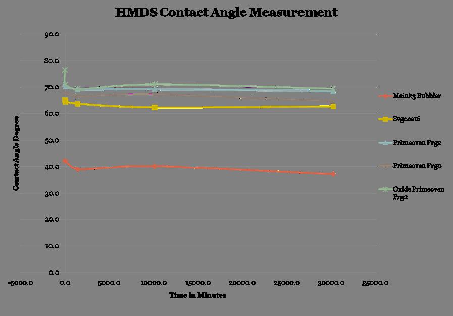
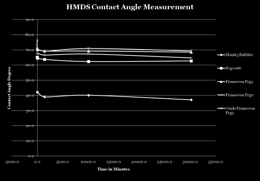
11 HMDS Methods of Application #1 Msink3 Bubbler Tank Does not dehydrate wafers Manually timed cycle 1 minute HMDS treatment Immediately hour later day later 39.0 NO heat 7 days later days later 37.1

12 HMDS Methods of Application Immediately 65.2 #2 Svgcoat6 1 minute HMDS treatment with N2 pump and purge cycles before application hot plate 100 C 1 hour later day later days later days later 62.7
13 HMDS Methods of Application #3 Primeoven Program 0 1 minute HMDS treatment with three N2 pump and purge cycles before application 90 C Immediately hour later day later days later days later 64.7
14 HMDS Methods of Application #4 Primeoven Program 2 2 minute HMDS treatment with one long pump down before application 90 C Immediately hour later day later days later days later 68.5


15 HMDS Methods of Application #5 Primeoven with Oxide Wafer 2 minute HMDS treatment with one long pump down before application 1000A oxide wafers Immediately hour later day later C 7 days later days later 69.4
16 HMDS Application Method Msink3 Bubbler for 1 minute 42.2 Contact Angle Measurement Taken Immediately Kruss Contact Angle Image Svgcoat6 for 1 minute 65.2 Primeoven Program 0 for 1 minute 67.7 Primeoven Program 2 for 2 minutes 71.1 Primeoven Program 2 on an Oxide Wafer for 2 minutes 76.5
17 Over Time
18
19 HMDS Application Conclusions Since the Svgcoat6 and Primeoven methods were baked, pumped and purged, the contact angles didn t degrade in 3 weeks because HMDS bonded with the oxide surface and sealed out moisture. Therefore, after HMDS treatment in the Svgcoat6 and Primeoven, it may still be possible to coat the photoresist on the wafers after 3 weeks. The Msink3 method did not bake the wafers nor did it pump out the extra water vapor. Therefore, the contact angle changed over time as the wafers absorbed some moisture.
20 Part B USING THE AMST TO DEPOSIT MONOLAYER FILM MEASURING CONTACT ANGLES

21 AMST Machine AMST is a molecular vapor deposition system that can deposit single layer mono-molecular films. Monolayer deposition is used to change the surface properties of MEMS and BioMEMS structures. Room temperature vapor deposition Sample Applications: Deposition of FOTS: increases surface hydrophobicity desired by MEMS devices Deposition of organosilane monolayers to enable covalent attachment of specific receptor molecules to BioMEMS sensor surfaces
22 AMST Available Gases Line 1 - deionized water vapor A small amount of water vapor is required for reaction of most chlorinated or oxy silanes to react with silica surfaces Line 2 - labmember proposed chemistries, our experiment used Gamma-methacryloxypropyltrimethoxysilane (Gamma-MPS) Line 3 Fluoro Octo Trichloro Silane (FOTS) Oxygen Used for substrate surface condition and chamber cleaning
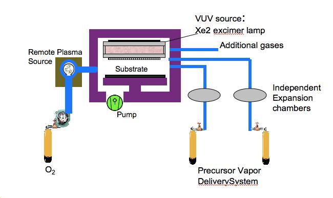
23 AMST Configuration

24 Steps for Using the AMST I. Vent chamber II. III. Open & Load wafer Run Process IV. Starts with Purge, followed by RF treatment, Vapor Injection, Process Reaction & final Purge cycles 25 minutes V. Vent chamber VI. Open & Remove wafer
25 Plasma Clean vs. Oxygen Clean Line RF Plasma Clean Clean Line Oxygen plasma to clean and pre-treat the substrate surface Plasma consists of a collection of free moving electrons and ions Removes impurities and contaminants from surfaces through the use of an energetic plasma Pump out lines by opening valves Turn on Ozone (O3) generator Flushes line and chamber to clean and prevent cross-contamination and ensure good film for deposition

26 MVD Coating with FOTS FOTS = fluoro octa trichloro silane FOTS treatment on SiO2 renders surface hydrophobic Water contact angle of 110 Proven anti-stiction coating for released MEMS Recipe Pretreatement Coating conditions RF Power 200 W Partial pressure of FOTS 4 T Oxygen 100 sccm Partial pressure of water 0.7 T Cleaning time 5 min Reaction time 15 min


27 MVD Coating with Gamma-MPS Gamma-MPS = gamma-methacryloxypropyltrimethoxysilane Gamma-MPS treatment on SiO2 improves hydrophobicity Water contact angle of 60 Used in coatings, adhesives and sealants to provide superior adhesion and durability Adhesion promoter for parylene Recipe Pretreatement Coating conditions Gamma-MPS RF Power 200 W Partial pressure of Gamma 0.5 T Oxygen 80 sccm Partial pressure of water 4 T Cleaning time 5 min Reaction time 15 min
28 FOTS Contact Angle Bare silicon wafers from the vendors have thin layers of native oxide After O2 plasma clean a thin layer of oxide of forms Silicon wafer out of box After AMST Plasma clean After Plasma clean & FOTS 20.1 o 0.0 o o
29 Unsuccessful Gamma-MPS Deposition 1. Performed 1 hour ozone clean on AMST 2. Purged Line 2 valve 10 times to flush out gas 1 process later Successful Deposition Unsuccessful Deposition Line 2 pressure not constant Leak Rate of 16.1 mtorr/min
30 Acknowledgements Thank you to everyone at the Nanolab for your help and guidance, and for making this a great summer. Thanks to Jimmy Chang, Anna Szucs, Sia Parsa, Rosemary Spivey, and the equipment engineers. Special thanks to Marilyn Kushner for taking me to Semicon, for the opportunity and the experience. Thank you Katalin Voros for this amazing summer opportunity. Special thanks to Kim Chan, an incredible mentor for whom I am so grateful!
Via Fill in Small Trenches using Hot Aluminum Process. By Alice Wong
 Via Fill in Small Trenches using Hot Aluminum Process By Alice Wong Goals for Project Good Via Fill in Small contact holes using hot aluminum process Be able to get good images of the contact holes using
Microelectronic Device Instructional Laboratory. Table of Contents
 Introduction Process Overview Microelectronic Device Instructional Laboratory Introduction Description Flowchart MOSFET Development Process Description Process Steps Cleaning Solvent Cleaning Photo Lithography
Yield Engineering Systems Product Guide
 Yield Engineering Systems Product Guide Yield Engineering Systems, Inc. Emerging Innovation Customer Dedication... Building Value and Trust for 30 Years! Yield Engineering Systems (YES) works closely with
Residual stress analysis of SiO films deposited by
 Ž. Surface and Coatings Technology 131 000 153 157 Residual stress analysis of SiO s deposited by plasma-enhanced chemical vapor deposition Jin-Kyung Choi a,, J. Lee a, Ji-Beom Yoo a, Jong-Sun Maeng b,
All fabrication was performed on Si wafers with 285 nm of thermally grown oxide to
 Supporting Information: Substrate preparation and SLG growth: All fabrication was performed on Si wafers with 285 nm of thermally grown oxide to aid in visual inspection of the graphene samples. Prior
Surface Micromachining
 Surface Micromachining Micro Actuators, Sensors, Systems Group University of Illinois at Urbana-Champaign Outline Definition of surface micromachining Most common surface micromachining materials - polysilicon
UTILIZATION OF ATMOSPHERIC PLASMA SURFACE PREPARATION TO IMPROVE COPPER PLATING PROCESSES.
 SESSION 14 MATERIALS AND PROCESSES FOR ADVANCED PACKAGING UTILIZATION OF ATMOSPHERIC PLASMA SURFACE PREPARATION TO IMPROVE COPPER PLATING PROCESSES. Eric Schulte 1, Gilbert Lecarpentier 2 SETNA Corporation
Fabrication of sub-100nm thick Nanoporous silica thin films
 Fabrication of sub-100nm thick Nanoporous silica thin films Abstract M. Ojha, W. Cho, J. L. Plawsky, W. N. Gill Department of chemical and biological engineering, Rensselaer Polytechnic Institute Low refractive
Photolithography I ( Part 2 )
") 1 Photolithography I ( Part 2 ) Chapter 13 : Semiconductor Manufacturing Technology by M. Quirk & J. Serda Bjørn-Ove Fimland, Department of Electronics and Telecommunication, Norwegian University of Science
1 Photolithography I ( Part 2 ) Chapter 13 : Semiconductor Manufacturing Technology by M. Quirk & J. Serda Bjørn-Ove Fimland, Department of Electronics and Telecommunication, Norwegian University of Science
A discussion of crystal growth, lithography, etching, doping, and device structures is presented in
 Chapter 5 PROCESSING OF DEVICES A discussion of crystal growth, lithography, etching, doping, and device structures is presented in the following overview gures. SEMICONDUCTOR DEVICE PROCESSING: AN OVERVIEW
A STUDY OF THE EFFECTIVENESS OF THE REMOVAL OF HYDROCARBON CONTAMINATION BY OXIDATIVE CLEANING INSIDE THE SEM.
 A STUDY OF THE EFFECTIVENESS OF THE REMOVAL OF HYDROCARBON CONTAMINATION BY OXIDATIVE CLEANING INSIDE THE SEM. Neal Sullivan, Tung Mai, Scott Bowdoin* and Ronald Vane** A poster paper presented at Microscopy
Simple Cubic Crystal
 Starting Material Simple Cubic Crystal Crystal Planes offset by d/4 Diamond lattice cell (C, Si, Ge, etc.) face atom in FCC corner atom in FCC (100) plane (110) plane (111) plane Crystal Planes/Direction
Regents of the University of California
 Surface-Micromachining Process Flow Photoresist Sacrificial Oxide Structural Polysilcon Deposit sacrificial PSG: Target = 2 m 1 hr. 40 min. LPCVD @450 o C Densify the PSG Anneal @950 o C for 30 min. Lithography
Micro-Electro-Mechanical Systems (MEMS) Fabrication. Special Process Modules for MEMS. Principle of Sensing and Actuation
 Fabrication. Special Process Modules for MEMS. Principle of Sensing and Actuation") Micro-Electro-Mechanical Systems (MEMS) Fabrication Fabrication Considerations Stress-Strain, Thin-film Stress, Stiction Special Process Modules for MEMS Bonding, Cavity Sealing, Deep RIE, Spatial forming
Micro-Electro-Mechanical Systems (MEMS) Fabrication Fabrication Considerations Stress-Strain, Thin-film Stress, Stiction Special Process Modules for MEMS Bonding, Cavity Sealing, Deep RIE, Spatial forming
A Deep Silicon RIE Primer Bosch Etching of Deep Structures in Silicon
 A Deep Silicon RIE Primer Bosch Etching of Deep Structures in Silicon April 2009 A Deep Silicon RIE Primer 1.0) Etching: Silicon does not naturally etch anisotropically in fluorine based chemistries. Si
Lecture Day 2 Deposition
 Deposition Lecture Day 2 Deposition PVD - Physical Vapor Deposition E-beam Evaporation Thermal Evaporation (wire feed vs boat) Sputtering CVD - Chemical Vapor Deposition PECVD LPCVD MVD ALD MBE Plating
Thin. Smooth. Diamond.
 UNCD Wafers Thin. Smooth. Diamond. UNCD Wafers - A Family of Diamond Material UNCD is Advanced Diamond Technologies (ADT) brand name for a family of thin fi lm diamond products. UNCD Aqua The Aqua series
Thin. Smooth. Diamond.
 UNCD Wafers Thin. Smooth. Diamond. UNCD Wafers - A Family of Diamond Material UNCD is Advanced Diamond Technologies (ADT) brand name for a family of thin fi lm diamond products. UNCD Aqua The Aqua series
Plasma-Enhanced Chemical Vapor Deposition
 Plasma-Enhanced Chemical Vapor Deposition Steven Glenn July 8, 2009 Thin Films Lab 4 ABSTRACT The objective of this lab was to explore lab and the Applied Materials P5000 from a different point of view.
EE C245 ME C218 Introduction to MEMS Design Fall 2011
 Lecture Outline EE C245 ME C218 Introduction to MEMS Design Fall 2011 Prof. Clark T.-C. Nguyen Dept. of Electrical Engineering & Computer Sciences University of California at Berkeley Berkeley, CA 94720
PEAK EFFICIENCIES WITH FALLING MANUFACTURING COSTS
 PEAK EFFICIENCIES WITH FALLING MANUFACTURING COSTS Simple and cost-effective introduction of PERC technology into the mass production of solar cells Kerstin Strauch, Florian Schwarz, Sebastian Gatz 1 Introduction
Photoresist Coat, Expose and Develop Laboratory Dr. Lynn Fuller
 ROCHESTER INSTITUTE OF TECHNOLOGY MICROELECTRONIC ENGINEERING Photoresist Coat, Expose and Develop Laboratory Dr. Lynn Fuller Webpage: http://www.rit.edu/lffeee 82 Lomb Memorial Drive Rochester, NY 14623-5604
Micro-Electro-Mechanical Systems (MEMS) Fabrication. Special Process Modules for MEMS. Principle of Sensing and Actuation
 Fabrication. Special Process Modules for MEMS. Principle of Sensing and Actuation") Micro-Electro-Mechanical Systems (MEMS) Fabrication Fabrication Considerations Stress-Strain, Thin-film Stress, Stiction Special Process Modules for MEMS Bonding, Cavity Sealing, Deep RIE, Spatial forming
Micro-Electro-Mechanical Systems (MEMS) Fabrication Fabrication Considerations Stress-Strain, Thin-film Stress, Stiction Special Process Modules for MEMS Bonding, Cavity Sealing, Deep RIE, Spatial forming
LAM4600 Plasma Etch Tool Recipes Dr. Lynn Fuller Webpage:
 ROCHESTER INSTITUTE OF TECHNOLOGY MICROELECTRONIC ENGINEERING LAM4600 Plasma Etch Tool Recipes Webpage: http://people.rit.edu/lffeee 82 Lomb Memorial Drive Rochester, NY 14623-5604 Tel (585) 475-2035 Email:
Chemical Vapor Deposition
 Preparation of Low-k Porous SiO 2 Films by SiO 2 /Organic Hybrid Chemical Vapor Deposition Akira Fujimoto and Osamu Sugiura Department of Physical Electronics, Tokyo Institute of Technology, 2-2-, O-okayama,
Report 1. B. Starting Wafer Specs Number: 10 Total, 6 Device and 4 Test wafers
 Aaron Pederson EE 432 Lab Dr. Meng Lu netid: abp250 Lab instructor: Yunfei Zhao Report 1 A. Overview The goal of this lab is to go through the semiconductor fabrication process from start to finish. This
Application Note. R*evolution III Remote Plasma Source: Low Particle Performance in O 2 / N 2. Photoresist Ashing PROBLEM. BACKGROUND R*evolution III
 R*evolution III Remote Plasma Source: Low Particle Performance in / Photoresist Ashing PROBLEM It is critical that the remote plasma sources used in semiconductor device processing be operated in a manner
Micro-Electro-Mechanical Systems (MEMS) Fabrication. Special Process Modules for MEMS. Principle of Sensing and Actuation
 Fabrication. Special Process Modules for MEMS. Principle of Sensing and Actuation") Micro-Electro-Mechanical Systems (MEMS) Fabrication Fabrication Considerations Stress-Strain, Thin-film Stress, Stiction Special Process Modules for MEMS Bonding, Cavity Sealing, Deep RIE, Spatial forming
Micro-Electro-Mechanical Systems (MEMS) Fabrication Fabrication Considerations Stress-Strain, Thin-film Stress, Stiction Special Process Modules for MEMS Bonding, Cavity Sealing, Deep RIE, Spatial forming
LAM4600 Plasma Etch Tool Recipes Dr. Lynn Fuller
 ROCHESTER INSTITUTE OF TECHNOLOGY MICROELECTRONIC ENGINEERING LAM4600 Plasma Etch Tool Recipes Dr. Lynn Fuller Webpage: http://people.rit.edu/lffeee 82 Lomb Memorial Drive Rochester, NY 14623-5604 Tel
Chapter 3 Silicon Device Fabrication Technology
 Chapter 3 Silicon Device Fabrication Technology Over 10 15 transistors (or 100,000 for every person in the world) are manufactured every year. VLSI (Very Large Scale Integration) ULSI (Ultra Large Scale
EE 527 MICROFABRICATION. Lecture 15 Tai-Chang Chen University of Washington EE-527 M4 MASK SET: NPN BJT. C (sub) A E = 40 µm x 40 µm
 A E = 40 µm x 40 µm") EE 527 MICROFABRICATION Lecture 15 Tai-Chang Chen University of Washington EE-527 M4 MASK SET: NPN BJT C (sub) E B A E = 40 µm x 40 µm 1 EE-527 M4 MASK SET: MOS C-V TEST CAPACITORS W = 10 µm L = 10 µm
EE 527 MICROFABRICATION Lecture 15 Tai-Chang Chen University of Washington EE-527 M4 MASK SET: NPN BJT C (sub) E B A E = 40 µm x 40 µm 1 EE-527 M4 MASK SET: MOS C-V TEST CAPACITORS W = 10 µm L = 10 µm
Device Fabrication: CVD and Dielectric Thin Film
 Device Fabrication: CVD and Dielectric Thin Film 1 Objectives Identify at least four CVD applications Describe CVD process sequence List the two deposition regimes and describe their relation to temperature
INTEGRATED-CIRCUIT TECHNOLOGY
 INTEGRATED-CIRCUIT TECHNOLOGY 0. Silicon crystal growth and wafer preparation 1. Processing Steps 1.1. Photolitography 1.2. Oxidation 1.3. Layer Deposition 1.4. Etching 1.5. Diffusion 1.6 Backend: assembly,
Procese de depunere in sistemul Plasma Enhanced Chemical Vapor Deposition (PECVD)
") Procese de depunere in sistemul Plasma Enhanced Chemical Vapor Deposition (PECVD) Ciprian Iliescu Conţinutul acestui material nu reprezintă in mod obligatoriu poziţia oficială a Uniunii Europene sau a
Procese de depunere in sistemul Plasma Enhanced Chemical Vapor Deposition (PECVD) Ciprian Iliescu Conţinutul acestui material nu reprezintă in mod obligatoriu poziţia oficială a Uniunii Europene sau a
Major Fabrication Steps in MOS Process Flow
 Major Fabrication Steps in MOS Process Flow UV light Mask oxygen Silicon dioxide photoresist exposed photoresist oxide Silicon substrate Oxidation (Field oxide) Photoresist Coating Mask-Wafer Alignment
MEMORANDUM I. OVERVIEW
 MEMORANDUM To: Katalin Voros, Operations Manager From: Sia Parsa, Process Engineering Manager Subject: 2009 Year-End Report Date: 25 January 2010 I. OVERVIEW This memorandum documents process engineering
General Introduction to Microstructure Technology p. 1 What is Microstructure Technology? p. 1 From Microstructure Technology to Microsystems
 General Introduction to Microstructure Technology p. 1 What is Microstructure Technology? p. 1 From Microstructure Technology to Microsystems Technology p. 9 The Parallels to Microelectronics p. 15 The
Wireless implantable chip with integrated Nitinol-based pump for radio-controlled local drug delivery
 Electronic Supplementary Material (ESI) for Lab on a Chip. This journal is The Royal Society of Chemistry 2014 Electronic Supplementary Information Wireless implantable chip with integrated Nitinol-based
Micro/Nano Technology Center University of Louisville. Dry Etch Capabilities. NNCI Etch Workshop May 24-25, 2016
 Micro/Nano Technology Center University of Louisville Dry Etch Capabilities NNCI Etch Workshop May 24-25, 2016 TRION METAL ETCHER MODEL: MINILOCK-PHANTOM III ICP/RIE Trion etcher uses 7 gasses for chemistry:
Today s Class. Materials for MEMS
 Lecture 2: VLSI-based Fabrication for MEMS: Fundamentals Prasanna S. Gandhi Assistant Professor, Department of Mechanical Engineering, Indian Institute of Technology, Bombay, Recap: Last Class What is
Plasma technology overview
 passionate about plasma Plasma technology overview What is plasma treatment? Plasma treatment has been an essential production tool for more than 30 years in the fabrication of microelectronic devices
Processing guidelines
 Processing guidelines mr-uvcur21 series UV-curable Polymer for UV-based Nanoimprint Lithography Characteristics mr-uvcur21 is a liquid UV-curable polymer system with low viscosity and high curing rate
Fiji Thermal and Plasma Atomic Layer Deposition System (ALD) By Ultratech (Cambridge)
 By Ultratech (Cambridge)") Fiji Thermal and Plasma Atomic Layer Deposition System (ALD) By Ultratech (Cambridge) PREPARED BY: You-Sheng (Wilson) Lin, Nanolab Staff 7-30-2013 Superusers: Steve Franz You-Sheng Lin Max Ho X68923 X68923
Fiji Thermal and Plasma Atomic Layer Deposition System (ALD) By Ultratech (Cambridge) PREPARED BY: You-Sheng (Wilson) Lin, Nanolab Staff 7-30-2013 Superusers: Steve Franz You-Sheng Lin Max Ho X68923 X68923
ECC Durable treatments for ceramic and glass surfaces
 3 ECC Durable treatments for ceramic and glass surfaces 3Innovation Easy Clean Coating 3ECC products are fluoropolymer based materials that chemically react with siliceous substrates Resulting in a durable,
History of Parylene. The Parylene Deposition Process
 History of Parylene Parylene development started in 1947, when Michael Szwarc discovered the polymer as one of the thermal decomposition products of a common solvent p-xylene at temperatures exceeding
Silicon Epitaxial CVD Want to create very sharp PN boundary grow one type layer on other in single crystal form High dopant layers on low dopant
 Silicon Epitaxial CVD Want to create very sharp PN boundary grow one type layer on other in single crystal form High dopant layers on low dopant substrate Creates latch up protection for CMOS Buried Epi
Metallization deposition and etching. Material mainly taken from Campbell, UCCS
 Metallization deposition and etching Material mainly taken from Campbell, UCCS Application Metallization is back-end processing Metals used are aluminum and copper Mainly involves deposition and etching,
LAM 490 Etch Recipes. Dr. Lynn Fuller
 ROCHESTER INSTITUTE OF TECHNOLOGY MICROELECTRONIC ENGINEERING LAM 490 Etch Recipes Dr. Lynn Fuller Professor, Webpage: http://people.rit.edu/lffeee 82 Lomb Memorial Drive Rochester, NY 14623-5604 Tel (585)
Atmospheric and Low Pressure Plasma treatments: a comparison
 Atmospheric and Low Pressure Plasma treatments: a comparison Outline Introduction What is Plasma? Atmospheric Plasma and Low Pressure Plasma treatment Experimental Results of contact angle measurements
Thin Film Gas Sensor. Nanoelectronics and MEMS Laboratory National Electronics and Computer Technology
 Ion-assisted E-beam E Evaporated Thin Film Gas Sensor A. Wisitsoraat,, A. A Tuantranont,, V. V Patthanasettakul, T. Lomas,, and P. Chindaudom Nanoelectronics and MEMS Laboratory National Electronics and
4. Thermal Oxidation. a) Equipment Atmospheric Furnace
 Equipment Atmospheric Furnace") 4. Thermal Oxidation a) Equipment Atmospheric Furnace Oxidation requires precise control of: temperature, T ambient gas, G time spent at any given T & G, t Vito Logiudice 34 4. Thermal Oxidation b) Mechanism
4. Thermal Oxidation a) Equipment Atmospheric Furnace Oxidation requires precise control of: temperature, T ambient gas, G time spent at any given T & G, t Vito Logiudice 34 4. Thermal Oxidation b) Mechanism
Si DRIE APPLICATION In Corial 210IL
 Si DRIE APPLICATION In Corial 210IL CORIAL 210IL ICP-RIE equipment for deep Si etching applications Enlarged functionality with capability to deep etch silicon, silicon carbide, glass, sapphire, and quartz
New Dual Magnetron Plasma Source Designed For Large Area Substrate Pretreatment and Oxide Film Deposition P. Morse, R. Lovro, M. Rost, and J.
 New Dual Magnetron Plasma Source Designed For Large Area Substrate Pretreatment and Oxide Film Deposition P. Morse, R. Lovro, M. Rost, and J. German, Road Map Source Design Theory of Operation Experimental
High Barrier Multi-Layer Parylene Coating
 High Barrier Multi-Layer Parylene Coating Technology overview Surface Technolgy 2018 Company Profile Swiss company founded in 1979 Experts in Parylene coating technology Parylene Equipment Export rate
WHEATON DUAL. Vial. Perfecting the science of sample protection
 WHEATON Perfecting the science of sample protection WHEATON DualFusion vials combine the best properties of glass, with the mechanical strength and the precision molding of plastic. The vials are engineered
Surface Micromachining
 Surface Micromachining Outline Introduction Material often used in surface micromachining Material selection criteria in surface micromachining Case study: Fabrication of electrostatic motor Major issues
Alternative Methods of Yttria Deposition For Semiconductor Applications. Rajan Bamola Paul Robinson
 Alternative Methods of Yttria Deposition For Semiconductor Applications Rajan Bamola Paul Robinson Origin of Productivity Losses in Etch Process Aggressive corrosive/erosive plasma used for etch Corrosion/erosion
micro resist technology
 Characteristics Processing guidelines Negative Tone Photoresist Series ma-n 2400 ma-n 2400 is a negative tone photoresist series designed for the use in micro- and nanoelectronics. The resists are available
! Easy spin coat application. 1 Because Federal, State, Local and International laws may
 CATIONIC PRIMING AGENT DOCUMENT ID: SP4T9906 SurPass 4000 is an advance aqueous based priming agent which provides maximum photoresist adhesion to a wide range of substrate materials. SurPass 4000 achieves
EE 5344 Introduction to MEMS. CHAPTER 3 Conventional Si Processing
 3. Conventional licon Processing Micromachining, Microfabrication. EE 5344 Introduction to MEMS CHAPTER 3 Conventional Processing Why silicon? Abundant, cheap, easy to process. licon planar Integrated
Alternative MicroFabrication and Applications in Medicine and Biology
 Alternative MicroFabrication and Applications in Medicine and Biology Massachusetts Institute of Technology 6.152 - Lecture 15 Fall 2003 These slides prepared by Dr. Hang Lu Outline of Today s Materials
Activities in Plasma Process Technology at SENTECH Instruments GmbH, Berlin. Dr. Frank Schmidt
 Activities in Plasma Process Technology at SENTECH Instruments GmbH, Berlin Dr. Frank Schmidt The Company Company Private company, founded 1990 80 employees ISO 9001 Location Science & Technology Park,
MCC. LOR Lift-Off Resists LOR RESISTS OFFER TYPES OF RESISTS
 MCC LOR RESISTS OFFER Submicron linewidth control Finely tuned undercuts Does not intermix with imaging resists (no scum) Excellent adhesion to Si, NiFe, GaAs, InP and many other III-V and II-VI materials
Advanced solar cell production requires a systems-level approach to achieve abatement goals
 Advanced solar cell production requires a systems-level approach to achieve abatement goals Words: Chris Jones, Senior Product Manager, Edwards Vacuum Solar panel manufacturers strive to minimize cost
Materials and Processing Issues Associated With Seal Coating Development
 Materials and Processing Issues Associated With Seal Coating Development J. D. Meyer and W. Y. Lee Department of Chemical, Biochemical, and Materials Engineering Stevens Institute of Technology 23 rd Annual
Single-digit-resolution nanopatterning with. extreme ultraviolet light for the 2.5 nm. technology node and beyond
 Electronic Supplementary Material (ESI) for Nanoscale. This journal is The Royal Society of Chemistry 205 Supplementary Information for: Single-digit-resolution nanopatterning with extreme ultraviolet
Silicon Epitaxial CVD Want to create very sharp PN boundary grow one type layer on other in single crystal form High dopant layers on low dopant
 Silicon Epitaxial CVD Want to create very sharp PN boundary grow one type layer on other in single crystal form High dopant layers on low dopant substrate Creates latch up protection for CMOS Buried Epi
Cures, Sealers Densifiers & Crystal Technology Ultimate / Proven Concrete Protection
 Cures, Sealers Densifiers & Crystal Technology Ultimate / Proven Concrete Protection IF USED CORRECTELY AND IN THE RIGHT PLACES What is a Curing Membrane? Aids in the development of the designed strength
Extending product lifetime with ALD moisture barrier
 Whitepaper Extending product lifetime with ALD moisture barrier 01 executive summary Atomic Layer Deposition (ALD) is a thin film technology that enables new and highly competitive products. Typical applications
Introduction of Plasma Indicator "PLAZMARK "
 SEMICON TAIWAN 2017 Introduction of Plasma Indicator "PLAZMARK " Thursday, September 14, 2017 Plasma Indicator Division SEISAKU OHSHIRO 1 Concept of Plasma Indicator An Evaluation tool made from functional
Self organization and properties of Black Silicon
 TECHNISCHE UNIVERSITÄT ILMENAU 51st IWK Internationales Wissenschaftliches Kolloquium September 11-15, 2006 Self organization and properties of Black Silicon M. Fischer, M. Stubenrauch, Th. Kups, H. Romanus,
Amorphous Silicon Solar Cells
 The Birnie Group solar class and website were created with much-appreciated support from the NSF CRCD Program under grants 0203504 and 0509886. Continuing Support from the McLaren Endowment is also greatly
Comparison of Atmospheric Plasma and Corona Treatments in Promoting Seal Strength
 Comparison of Atmospheric Plasma and Corona Treatments in Promoting Seal Strength Presented by Rory Wolf Business Unit Manager ITW Pillar Technologies Discussion Agenda o Study Objective o Extrusion Coating
Thin AC-PDP Vacuum In-line Sealing Using Direct-Joint Packaging Method
 H128 0013-4651/2004/151 5 /H128/5/$7.00 The Electrochemical Society, Inc. Thin AC-PDP Vacuum In-line Sealing Using Direct-Joint Packaging Method Duck-Jung Lee, a,b,z Seung-IL Moon, a Yun-Hi Lee, c and
RainMaker Humidification System for Precise Delivery of Water Vapor into Atmospheric and Vacuum Applications
 RainMaker Humidification System for Precise Delivery of Water Vapor into Atmospheric and Vacuum Applications By Jeffrey Spiegelman Water vapor has multiple applications across industries including semiconductor,
Morphology and High-temperature Stability of Amorphous Alumina Coatings Deposited on Si and CeO 2 -Stabilized ZrO 2 by MOCVD
 Morphology and High-temperature Stability of Amorphous Alumina Coatings Deposited on Si and CeO 2 -Stabilized ZrO 2 by MOCVD J. D. Meyer and W. Y. Lee Dept. of Materials Science & Engineering Stevens Institute
PRESSURE SENSOR MODEL ACTIVITY. Pressure Sensor Model Activity
 PRESSURE SENSOR MODEL ACTIVITY Pressure Sensor Model Activity Unit Overview This activity uses household materials to build a pressure sensor Wheatstone Bridge sensing circuit Flexible diaphragm Reference
Supporting Information: Model Based Design of a Microfluidic. Mixer Driven by Induced Charge Electroosmosis
 Supporting Information: Model Based Design of a Microfluidic Mixer Driven by Induced Charge Electroosmosis Cindy K. Harnett, Yehya M. Senousy, Katherine A. Dunphy-Guzman #, Jeremy Templeton * and Michael
PLASMA TREATMENT OF X-Wire. Insulated Bonding Wire
 PLASMA TREATMENT OF X-Wire Insulated Bonding Wire Application Note Published by: March Plasma Systems www.marchplasma.com and Microbonds Inc. www.microbonds.com 2007 Microbonds Inc. and March Plasma Systems
ANTI-STICTION COATINGS FOR HIGH RELIABILITY MEMS
 ANTI-STICTION COATINGS FOR HIGH RELIABILITY MEMS Introduction Nilesh Gunda, Santosh K. Jha and Suri A. Sastri Surmet Corporation, 33 B Street Burlington, MA 01803 (USA). Micro-electromechanical system
PHYS 534 (Fall 2008) Process Integration OUTLINE. Examples of PROCESS FLOW SEQUENCES. >Surface-Micromachined Beam
 Process Integration OUTLINE. Examples of PROCESS FLOW SEQUENCES. >Surface-Micromachined Beam") PHYS 534 (Fall 2008) Process Integration Srikar Vengallatore, McGill University 1 OUTLINE Examples of PROCESS FLOW SEQUENCES >Semiconductor diode >Surface-Micromachined Beam Critical Issues in Process
PHYS 534 (Fall 2008) Process Integration Srikar Vengallatore, McGill University 1 OUTLINE Examples of PROCESS FLOW SEQUENCES >Semiconductor diode >Surface-Micromachined Beam Critical Issues in Process
ECE 440 Lecture 27 : Equilibrium P-N Junctions I Class Outline:
 ECE 440 Lecture 27 : Equilibrium P-N Junctions I Class Outline: Fabrication of p-n junctions Contact Potential Things you should know when you leave Key Questions What are the necessary steps to fabricate
Parylene: what is it?
 Parylene: what is it? Parylene is a protective polymer material, which is transparent and colourless. It is a MIL-I-46058C and UL approved conformal coating listed as Type XY. Parylene is applied by a
X-ray Photoelectron Spectroscopy
 X-ray Photoelectron Spectroscopy X-ray photoelectron spectroscopy (XPS) is a non-destructive technique used to analyze the elemental compositions, chemical and electronic states of materials. XPS has a
Kinetics of Silicon Oxidation in a Rapid Thermal Processor
 Kinetics of Silicon Oxidation in a Rapid Thermal Processor Asad M. Haider, Ph.D. Texas Instruments Dallas, Texas USA Presentation at the National Center of Physics International Spring Week 2010 Islamabad
SELECTION GUIDE Sample Transport Tubing
 SELECTION GUIDE Sample Transport Tubing A guide for the selection of sample transport tubing. Tube Selection for Analyzer Sample Systems Selecting the optimum process tube for use in analyzer sample transport
AC : MICROWAVE PLASMA CLEANER DESIGN FOR SEMI- CONDUCTOR FABRICATION AND MATERIALS PROCESSING LABO- RATORY USE
 AC 2011-2416: MICROWAVE PLASMA CLEANER DESIGN FOR SEMI- CONDUCTOR FABRICATION AND MATERIALS PROCESSING LABO- RATORY USE Mustafa G. Guvench, University of Southern Maine Mustafa G. Guvench received M.S.
University of Minnesota Nano Center Standard Operating Procedure
 Equipment Name: University of Minnesota Nano Center PECVD Coral Name: pecvd Revision Number: 2.0 Model: Plasmatherm 340 Revisionist: Mark Fisher Location: Bay 3 Date: 20 Sept 2013 1 Description The Plasmatherm
Si, SiGe and Ge Epitaxial CVD Systems
 Si, SiGe and Ge Epitaxial CVD Systems To Whom It May Concern This is an RFQ (Request for Quote) document for procurement of an epitaxial CVD system along with attachments as part of a tender for the Centre
Lab #2 Wafer Cleaning (RCA cleaning)
") Lab #2 Wafer Cleaning (RCA cleaning) RCA Cleaning System Used: Wet Bench 1, Bay1, Nanofabrication Center Chemicals Used: H 2 O : NH 4 OH : H 2 O 2 (5 : 1 : 1) H 2 O : HF (10 : 1) H 2 O : HCl : H 2 O 2
Lab #2 Wafer Cleaning (RCA cleaning) RCA Cleaning System Used: Wet Bench 1, Bay1, Nanofabrication Center Chemicals Used: H 2 O : NH 4 OH : H 2 O 2 (5 : 1 : 1) H 2 O : HF (10 : 1) H 2 O : HCl : H 2 O 2
Molecular Vapor Deposition and Patterning of Organosilane Self- Assembled Monolayers for Directed Growth of Neuron Cells.
 EE 412 2014 Spring Quarter Final Report Molecular Vapor Deposition and Patterning of Organosilane Self- Assembled Monolayers for Directed Growth of Neuron Cells. Felix Alfonso & Hsin-Ya Lou Mentor : Michelle
Surface Modification: How low-pressure plasma treatments can benefit your manufacturing process
 Surface Modification: How low-pressure plasma treatments can benefit your manufacturing process surface modification Surface modification is growing exponentially as industrial engineers and manufacturers
Q1. The data in the table below show the melting points of oxides of some Period 3 elements. O 10 O P (Extra space) (2)......
 (2)......") Q1. The data in the table below show the melting points of oxides of some Period 3 elements. Na 2 O P 4 O 10 SO 2 T m /K 1548 573 200 (a) In terms of structure and bonding, explain why (i) sodium oxide
Q1. The data in the table below show the melting points of oxides of some Period 3 elements. Na 2 O P 4 O 10 SO 2 T m /K 1548 573 200 (a) In terms of structure and bonding, explain why (i) sodium oxide
STRESS IN SU-8 PHOTORESIST FILMS: DOE APPROACH
 STRESS IN SU-8 PHOTORESIST FILMS: DOE APPROACH RYAN M. BOWEN, EYUP CINAR 02/23/2012 0305-320 Design of Experiments Overview Motivation Introduction Theory - Negative Photoresist Deposition Process Experimental
Fabrication Technology
 Fabrication Technology By B.G.Balagangadhar Department of Electronics and Communication Ghousia College of Engineering, Ramanagaram 1 OUTLINE Introduction Why Silicon The purity of Silicon Czochralski
Photolithography Process Technology
 Contents Photolithography Process - Wafer Preparation - Photoresist Coating - Align & Expose - Photoresist Development Process Control CD Measurement Equipment Expose System & Wafer Track Consumables Chemicals
Thermal Evaporation. Theory
 Thermal Evaporation Theory 1. Introduction Procedures for depositing films are a very important set of processes since all of the layers above the surface of the wafer must be deposited. We can classify
Chapter 5 Thermal Processes
 Chapter 5 Thermal Processes 1 Topics Introduction Hardware Oxidation Diffusion Annealing Post-Implantation Alloying Reflow High Temp CVD Epi Poly Silicon Nitride RTP RTA RTP Future Trends 2 Definition
Using Argon Plasma to Remove Fluorine, Organic and Metal Oxide Contamination for Improved Wire Bonding Performance
 Using Argon Plasma to Remove Fluorine, Organic and Metal Oxide Contamination for Improved Wire Bonding Performance Scott D. Szymanski March Plasma Systems Concord, California, U.S.A. sszymanski@marchplasma.com
Serving Clients SINCE 1998
 Serving Clients SINCE 1998 Deva Preservation Services O&G, OFFSHORE, ENERGY, TRANSPORT SECTOR 1 Deva Management Services - Managing FPSO / FSO / Semi-submersible conversion & modification projects - Focus: