MODEL PicoMill TEM specimen preparation system. Achieve ultimate specimen quality free from amorphous and implanted layers
|
|
|
- Samuel Wood
- 6 years ago
- Views:
Transcription
1
 milling is a widely used technique for today s cutting-edge materials that provides a means to prepare")
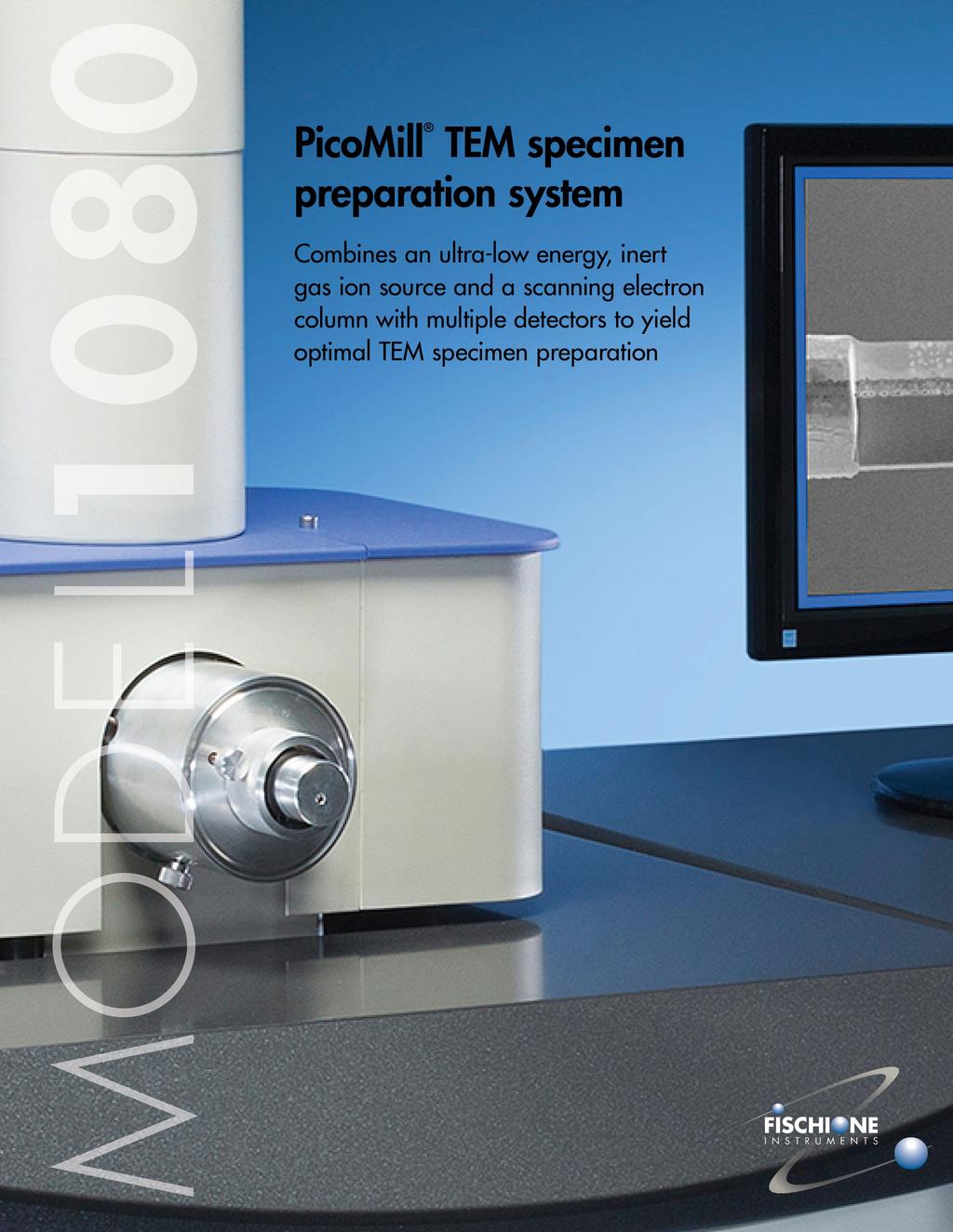
2 MODEL 1080 PicoMill TEM specimen preparation system Combines an ultra-low energy, inert gas ion source, and a scanning electron column with multiple detectors to yield optimal TEM specimens. POST-FIB PROCESSING PRODUCES THE HIGHEST QUALITY TEM SPECIMENS Focused ion beam (FIB) milling is a widely used technique for today s cutting-edge materials that provides a means to prepare transmission electron microscopy (TEM) specimens. The challenge in working with these advanced materials is to create specimens that are electron transparent and are free from artifacts. The FIB is highly effective in preparing TEM specimens, but the use of a high-energy, liquid metal ion source can often result in specimen amorphization, gallium implantation, or both. Achieve ultimate specimen quality free from amorphous and implanted layers Complements FIB technology Milling without introduction of artifacts Advanced detector technology for imaging and precise endpoint detection In situ imaging with ions and electrons Microscope connectivity for risk-free specimen handling Adds capability and capacity Fast, reliable, and easy to use The PicoMill system is the ideal complement to FIB technology; it adds the increased capability of producing optimal specimen quality while enhancing the overall specimen preparation throughput by moving final thinning offline.


3 A history of specimen preparation innovation Since 2006, Fischione Instruments revolutionary NanoMill has set the standard for high-quality TEM specimen preparation. The NanoMill system s unique combination of features ultra-low energy ion source, low-angle milling capabilities, and submicron ion beam diameter have been critical for uncovering specific features of interest within TEM specimens. The NanoMill system has produced specimens with optimal quality for a number of research and industrial applications, including oxides, fuel cells, photovoltaics, battery materials, and many others. For microelectronic and semiconductor applications, the NanoMill system s capabilities have played a critical role in producing pristine TEM specimens. Since the introduction of the NanoMill system, the microelectronics industry has continued to develop products that are increasingly smaller in size and increasingly complex in geometry, such as three-dimensional FinFET gate architectures and vertical NAND gates. These intricate devices are comprised of varying densities of dissimilar materials with structures that can contain compounds, such as repeating layers of oxides, silicides, nitrides, various metals, and a mix of high-k and low-k dielectric materials. These structures contain materials with very different atomic numbers, which can result in differing sputter rates. Preparing these unique specimens for high-resolution imaging by TEM has been consistently achieved with the NanoMill system s advanced technology. Decreased device sizes coupled with increased materials complexity demand the next generation of TEM specimen preparation. Drawing on our history of innovation, Fischione Instruments developed the PicoMill TEM specimen preparation system, taking the NanoMill system technology to the highest possible level. Fischione Instruments Model 1080 PicoMill. 3
4 Designed specifically to integrate into a FIB workflow Focused ion beam (FIB) technology is frequently the choice for creating TEM specimens. The FIB is used to create a site-specific, extremely thin lamella that is extracted and mounted to a supporting grid for TEM imaging and analysis. The FIB is highly effective in preparing TEM specimens; however, the FIB s liquid metal (gallium) ion source can result in amorphization, gallium implantation, or both. These damaged layers can be as thick as 10 to 30 nm. The FIB process is often started at high kilovolt energy levels and the voltage is decreased as the lamella thins. For very low-energy FIB applications, the operator may need to refocus the instrument and realign the beam. This can slow down the overall processing time per specimen. In addition, even low-voltage milling with the FIB may result in gallium implantation. The PicoMill system is ideally suited to removing these damaged layers. It offers the key features of the NanoMill system ultra-low energy, inert gas ion source, low-angle milling capabilities, and submicron ion beam diameter with the added capability of a scanning electron column and multiple detectors. The scanning electron column provides the ability to image a lamella at a scale that is sufficient to view the features of interest. Let the FIB do what the FIB does best; let the PicoMill system do the rest To maximize FIB capacity, specimens can be moved offline for final thinning on the PicoMill system. The PicoMill system provides the ability to precisely and predictably thin a specimen, which reduces the potential for rework and optimizes specimen processing time. This increases your capability by producing specimens of superior quality and enhances the overall specimen preparation throughput. The PicoMill system will allow you to achieve first time right specimen preparation every time. THE IDEAL COMPLEMENT TO FIB TECHNOLOGY By moving final specimen thinning offline, you increase the capability of producing optimal specimen quality while enhancing overall specimen preparation throughput. FIB Lamella is prepared by FIB and mounted to a supporting grid. PicoMill system The grid with lamella is mounted on the PicoMill specimen holder. The specimen holder is then inserted into the PicoMill system goniometer for final thinning by ion milling. TEM PicoMill holder with specimen is plasma cleaned and then inserted into the TEM for imaging and analysis. Result Improved specimen quality and enhanced throughput. From FIB to PicoMill system to TEM A FIB-prepared lamella is mounted on a supporting grid and is loaded onto the PicoMill specimen holder, a TEM-style holder that can be used in both the PicoMill system and the TEM. The design of the holder allows for positive and negative tilt ion milling of the specimen in the PicoMill system and facilitates imaging of the specimen in the TEM. Following pre-pump of the PicoMill system s standard side-entry goniometer, the specimen holder is inserted into the chamber and the specimen is positioned accordingly for ion milling operations and scanning electron microscope (SEM) imaging. 4
 and has an operating voltage range of 50 ev to 2 kv.")
5 Site-specific, ultra-low-energy milling The PicoMill system s ion source features a filament-based ionization chamber and electrostatic lenses. The ion source was specifically developed to produce ultra-low ion energies with a submicron ion beam diameter. It uses inert gas (argon) and has an operating voltage range of 50 ev to 2 kv. The ion source s feedback control algorithm automatically produces stable and repeatable ion beam conditions over a wide variety of milling parameters. Redeposition of sputtered material onto the area of interest is avoided because the ion beam can be focused to a specific area. You can scan a region of the specimen s surface or target a specific area for selective milling. The ions only contact the site of interest on the specimen where they are needed to do the work. The ion beam is kept away from the grid, which prevents redeposition. Precise milling angle adjustment The ion beam impingement angle is programmable from -15 to +90. The ion source is fixed in position and the goniometer tilts the specimen holder to achieve the programmed milling angle through the PicoMill system user interface. The specimen is positioned along the X, Y, and Z axes to precisely orient the FIB lamella with respect to the ion and electron beams. Milling specimens at a low angle of incidence (less than 10 ) minimizes damage and specimen heating. Because low-angle milling, combined with ion beam rasterizing, facilitates uniform thinning of dissimilar materials, it is highly beneficial when preparing layered structures or composite materials. In situ imaging To complement the scanning electron column, the PicoMill system has multiple detectors: A backscatter electron detector (BSE) and a secondary electron detector (SED) for in situ imaging with ions and electrons A scanning/transmission electron detector (STEM) for electron transparency and endpoint detection The detector combination allows you to perform in situ imaging of the specimen before, during, and after ion milling. The grid containing a FIB lamella or a specific site on a conventionally prepared specimen can be imaged. FIB LAMELLA IN PICOMILL SYSTEM The PicoMill system allows the operator to choose a specific area of interest for selective milling via a submicron-sized ion beam. The red raster box indicates the selected milling area. The ion beam can be targeted away from the grid, which reduces the likelihood of redeposition. 5


6 You can view specimens in situ on a dedicated monitor that displays both electron- and ioninduced secondary electron images. Image capture is as simple as a click of a mouse. Computer control The PicoMill system is controlled via an intuitive user interface. You enter all milling parameters through the interface, such as milling angle, specimen position, and processing time. SEM control and detector selection are also user controlled. End-point detection/process termination A specimen prepared with optimal electron transparency is the ultimate goal for the best quality TEM imaging and analysis. This is particularly key when employing today s aberration corrected TEM technology. As the specimen thins, electron transmission increases and the leading edge recedes, which allows the STEM detector to provide end point information. The PicoMill system is also capable of time-based termination or it can be stopped manually. Plasma cleaning For the PicoMilling SM process, Fischione highly recommends that you plasma clean the specimen and specimen holder prior to insertion into the TEM. During fine-probe microanalysis, organic contamination may build up on the specimen. A cleaning time of 10 seconds to 2 minutes in the Fischione Model 1020 Plasma Cleaner or Model 1070 NanoClean removes the contamination without altering the specimen s structure or composition. Longer cleaning times can remove contamination caused by previous TEM viewing of specimens that were not plasma cleaned. Microscope connectivity reduces specimen handling The ability to use the same holder in the PicoMill system and the TEM means that you can quickly and safely transport the milled specimen from the PicoMill system to the TEM, which is particularly advantageous when you are working with one-of-a-kind specimens. TEM-STYLE HOLDER The PicoMill specimen holder was designed specifically for the PicoMill system. The design of the holder tip (top) allows positive and negative tilt ion milling of the specimen. The PicoMill specimen holder is inserted into the PicoMill system s side-entry goniometer (middle). The specimen holder can then go directly from the PicoMill system into the TEM for imaging and analysis (bottom). 6
 with Cs correction is shown.")


7 3D STRUCTURES REVEALED FinFET specimens prepared with the PicoMill system reveal three-dimensional structures for TEM imaging and analysis. A 22 nm Ivy Bridge microstructure imaged in a 300 kv scanning transmission electron microscope (STEM) with Cs correction is shown. Additional features Automatic gas control Gas is regulated automatically using precision mass flow technology. The low-flow ion source results in minimal gas consumption. Contamination-free, dry vacuum system The PicoMill system s fully integrated vacuum system includes a turbomolecular drag pump backed by a multistage diaphragm pump. This oil-free system assures a clean environment for specimen processing. The vacuum chamber is under constant vacuum, which means that ion milling can begin almost immediately after specimen insertion into the goniometer. Customer service that you can rely on Fischione Service is always there for you and is dedicated to delivering exceptional customer service. Fischione Service provides onsite installation and operations training, onsite preventive maintenance and repair, and replacement parts and supplies. Be sure to protect your investment and your budget with a service contract to reduce the risk of unexpected repair costs and instrument downtime. Fischione Instruments offers service contract options for the level of coverage, and peace of mind, that you need. To view the service contract options, go to: For questions regarding service of your Fischione products, contact service@fischione.com. E.A. Fischione Instruments, Inc Corporate Circle Export, PA USA Tel: Fax: info@fischione.com The PicoMill and NanoMill TEM specimen preparation systems are the subject of United States Patent Nos. 7,132,673 and 7,504,623. Other patents pending. NanoMill and PicoMill are registered trademarks of E.A. Fischione Instruments, Inc. PicoMilling is a service mark of E.A. Fischione Instruments, Inc E.A. Fischione Instruments, Inc. All rights reserved. Document Number PB1080 Revision 01 11/2014 Fischione products are designed and manufactured in Export, PA USA.
MODEL NanoMill TEM Specimen Preparation System. Ultra-low-energy, inert-gas ion source. Concentrated ion beam with scanning capabilities
 MODEL 1040 NanoMill TEM Specimen Preparation System The NanoMill system uses an ultra-low energy, concentrated ion beam to produce the highest quality specimens for transmission electron microscopy. Ultra-low-energy,
Specimen configuration
 APPLICATIONNOTE Model 1040 NanoMill TEM specimen preparation system Specimen configuration Preparing focused ion beam (FIB) milled specimens for submission to Fischione Instruments. The Model 1040 NanoMill
MODEL 1051 TEM Mill ION MILLING. Ion milling is used on physical science. specimens to reduce thickness to electron
 MODEL 1051 TEM Mill A state-of-the-art ion milling and polishing system offering reliable, high performance specimen preparation. It is compact, precise, and consistently produces high-quality transmission
MODEL SEM Mill. Two independently adjustable TrueFocus ion sources
 MODEL 1060 SEM Mill A state-of-the-art ion milling and polishing system. It is compact, precise, and consistently produces high-quality scanning electron microscopy (SEM) samples for a wide variety of
MODEL TEM Mill. Two independently adjustable TrueFocus ion sources
 MODEL 1050 TEM Mill A state-of-the-art ion milling and polishing system. It is compact, precise, and consistently produces high-quality transmission electron microscopy (TEM) specimens with large electron
MODEL 1061 SEM Mill ION MILLING. Ion milling is used in the physical. sciences to enhance the sample s surface. characteristics. Inert gas, typically
 MODEL 1061 SEM Mill A state-of-the-art ion milling and polishing system. It is compact, precise, and consistently produces high-quality scanning electron microscopy (SEM) samples in the shortest amount
MODEL Plasma Cleaner. Simultaneously cleans specimen and specimen holder. Cleans highly contaminated specimens in 2 minutes or less
 MODEL 1020 Plasma Cleaner Cleans specimens immediately before they are inserted into the electron microscope; removes existing carbonaceous debris from the specimen and prevents contamination from occurring
Model TEM Mill. Tabletop precision preparation for producing high-quality TEM specimens from a wide variety of materials EXCELLENCE MAGNIFIED
 Model 1050 TEM Mill Tabletop precision preparation for producing high-quality TEM specimens from a wide variety of materials EXCELLENCE MAGNIFIED Modular design for basic instrument operation or fully
A New Development to Eliminate Artifacts during TEM Sample Preparation in the FIB
 Inspire Innovation Through Collaboration High Technologies America, Inc. A New Development to Eliminate Artifacts during TEM Sample Preparation in the FIB (Un)traditional FIB Preparation A Common Problem
METHOD FOR IMPROVING FIB PREPARED TEM SAMPLES BY VERY LOW ENERGY Ar + ION MILL POLISHING
 METHOD FOR IMPROVING FIB PREPARED TEM SAMPLES BY VERY LOW ENERGY Ar + ION MILL POLISHING Yaron Kauffmann, Tzipi Cohen-Hyams, Michael Kalina, Hila Sadan-Meltzman and Wayne D. Kaplan Dept. of Materials Engineering
Model Plasma Cleaner. Effectively cleans specimens for electron microscopy EXCELLENCE MAGNIFIED
 Model 1020 Plasma Cleaner Effectively cleans specimens for electron microscopy EXCELLENCE MAGNIFIED Model 1020 Plasma Cleaner Simultaneously cleans specimen and specimen holder. Cleans highly contaminated
Specimen Preparation Technique for a Microstructure Analysis Using the Focused Ion Beam Process
 Specimen Preparation Technique for a Microstructure Analysis Using the Focused Ion Beam Process by Kozue Yabusaki * and Hirokazu Sasaki * In recent years the FIB technique has been widely used for specimen
Application Note. Sample Protection prior to FIB Processing. related instruments: Leica EM ACE600. Material Research. Life Science Research
 Material Life Science Application Note Sample Protection prior to FIB Processing related instruments: Leica EM ACE600 Medical Industrial Manufacturing Natural Resources 2 Each Atom Really Counts: Protect
3D Nano-analysis Technology for Preparing and Observing Highly Integrated and Scaled-down Devices in QTAT
 Hitachi Review Vol. 54 (2005), No. 1 27 3D Nano-analysis Technology for Preparing and Observing Highly Integrated and Scaled-down Devices in QTAT Toshie Yaguchi Takeo Kamino Tsuyoshi Ohnishi Takahito Hashimoto
zyvex TEM Sample Lift-out Using the Zyvex Nanoprober System By Kimberly Tuck, Zyvex Corporation
 TEM Sample Lift-out Using the Zyvex Nanoprober System By Kimberly Tuck, Zyvex Corporation Introduction The Zyvex Nanoprober System, coupled with a focused ion beam (FIB) tool, is a complete solution for
JSM-7800F Field Emission Scanning Electron Microscope
 JSM-7800F catalogue JSM-7800F Field Emission Scanning Electron Microscope We provide high performance The Ultimate Research Tool for Multi-Disciplinary Research Institutions Extreme resolution The super
Transzmissziós és pásztázó elektronmikroszkópos minták készítése ionsugaras vékonyítással
 Transzmissziós és pásztázó elektronmikroszkópos minták készítése ionsugaras vékonyítással Radi Zsolt Technoorg Linda Kft., Budapest Oktatói és Doktorandusz Konferencia Visegrád, 2012 State-of-the-art materials
A discussion of crystal growth, lithography, etching, doping, and device structures is presented in
 Chapter 5 PROCESSING OF DEVICES A discussion of crystal growth, lithography, etching, doping, and device structures is presented in the following overview gures. SEMICONDUCTOR DEVICE PROCESSING: AN OVERVIEW
Micro-Nano Fabrication Research
 Micro-Nano Fabrication Research Technical Education Quality Improvement Programme 22-23 December 2014 Dr. Rakesh G. Mote Assistant Professor Department of Mechanical Engineering IIT Bombay rakesh.mote@iitb.ac.in;
The principles and practice of electron microscopy
 The principles and practice of electron microscopy Second Edition Ian M. Watt CAMBRIDGE UNIVERSITY PRESS Contents Preface tofirstedition page ix Preface to second edition xi 1 Microscopy with light and
Focused Ion Beam CENTRE INTERDISCIPLINAIRE DE MICROSCOPIE ELECTRONIQUE. Marco Cantoni, EPFL-CIME CIME ASSEMBLEE GENERALE 2007
 Focused Ion Beam @ CENTRE INTERDISCIPLINAIRE DE MICROSCOPIE ELECTRONIQUE Present situation and vision Marco Cantoni, EPFL-CIME Dual Beam Nova 600 Nanolab from FEI Company FE-SEM & FIB: Ga LMIS 4 Gas Injector
A NEW APPROACH TO STUDYING CAST CB2 STEEL USING SLOW AND VERY SLOW ELECTRONS
 A NEW APPROACH TO STUDYING CAST CB2 STEEL USING SLOW AND VERY SLOW ELECTRONS Šárka Mikmeková 1 Josef Kasl 2 Dagmar Jandová 2 Ilona Müllerová 1 Luděk Frank 1 1 Institute of Scientific Instruments of the
STUDY & ANALYSIS OF ALUMINIUM FOIL AND ANATASE TITANIUM OXIDE (TiO2) USING TRANSMISSION ELECTRON MICROSCOPY
 USING TRANSMISSION ELECTRON MICROSCOPY") STUDY & ANALYSIS OF ALUMINIUM FOIL AND ANATASE TITANIUM OXIDE (TiO2) USING TRANSMISSION ELECTRON MICROSCOPY Ayush Garg Department of Chemical and Materials Engineering, University of Auckland, Auckland,
STUDY & ANALYSIS OF ALUMINIUM FOIL AND ANATASE TITANIUM OXIDE (TiO2) USING TRANSMISSION ELECTRON MICROSCOPY Ayush Garg Department of Chemical and Materials Engineering, University of Auckland, Auckland,
Product Information Version 2.0. ZEISS ORION NanoFab Three Ion Beams for Enhanced Flexibility in Sub-10 nm Fabrication
 Product Information Version 2.0 ZEISS ORION NanoFab Three Ion Beams for Enhanced Flexibility in Sub-10 nm Fabrication Three Ion Beams for Enhanced Flexibility in Sub-10 nm Fabrication Fabricate sub-10
A STUDY OF THE EFFECTIVENESS OF THE REMOVAL OF HYDROCARBON CONTAMINATION BY OXIDATIVE CLEANING INSIDE THE SEM.
 A STUDY OF THE EFFECTIVENESS OF THE REMOVAL OF HYDROCARBON CONTAMINATION BY OXIDATIVE CLEANING INSIDE THE SEM. Neal Sullivan, Tung Mai, Scott Bowdoin* and Ronald Vane** A poster paper presented at Microscopy
 LA-UR-01-3685 Approved for public release; distribution is unlimited. Title: USING A MULTI-DISCIPLINARY APPROACH, THE FIRST ELECTRON BACKSCATTERED KIKUCHI PATTERNS WERE CAPTURED FOR A PLUTONIUM ALLOY Author(s):
Electron Microscopy Sciences
 Electron Microscopy Sciences INSTRUCTIONAL MANUAL CAT. 80058-ST X-Checker Standard CAT. 80058-BN X-Checker Boron Nitride CAT. 80058-EX X-Checker Extra P.O. Box 550 s1560 Industry Road s Hatfield PA 19440
Simple method for formation of nanometer scale holes in membranes. E. O. Lawrence Berkeley National Laboratory, Berkeley, CA 94720
 Simple method for formation of nanometer scale holes in membranes T. Schenkel 1, E. A. Stach, V. Radmilovic, S.-J. Park, and A. Persaud E. O. Lawrence Berkeley National Laboratory, Berkeley, CA 94720 When
Transmission Electron Microscopy (TEM) Prof.Dr.Figen KAYA
 Prof.Dr.Figen KAYA") Transmission Electron Microscopy (TEM) Prof.Dr.Figen KAYA Transmission Electron Microscope A transmission electron microscope, similar to a transmission light microscope, has the following components along
Transmission Electron Microscopy (TEM) Prof.Dr.Figen KAYA Transmission Electron Microscope A transmission electron microscope, similar to a transmission light microscope, has the following components along
Differentially pumped quadrupole SIMS probe on FIBbased and two-beam microscopes
 Differentially pumped quadrupole SIMS probe on FIBbased and two-beam microscopes Richard J Chater (1), Barbara Shollock (1), David McPhail (1), Alan J Smith (2) and Graham Cooke (2) (1) Department of Materials,
From Eye to Insight. Leica EM ACE. Coater Family
 From Eye to Insight Leica EM ACE Coater Family EM ACE COATERS A Coater Family to cover all your needs. Developed in cooperation with leading scientists, the EM ACE coaters cover all the requirements for
Silver Diffusion Bonding and Layer Transfer of Lithium Niobate to Silicon
 Chapter 5 Silver Diffusion Bonding and Layer Transfer of Lithium Niobate to Silicon 5.1 Introduction In this chapter, we discuss a method of metallic bonding between two deposited silver layers. A diffusion
INDIAN INSTITUTE OF SCIENCE EDUCATION AND RESEARCH PUNE
 INDIAN INSTITUTE OF SCIENCE EDUCATION AND RESEARCH PUNE CLARIFICATION ON TENDER NUMBER - IISER-PUR-0458-16 ITEM DESCRIPTION- PROCUREMENT OF HIGH RESOLUTION TRANSMISSION ELECTRON MICROSCOPE Refer our Press
Transmission Kikuchi Diffraction in the Scanning Electron Microscope
 Transmission Kikuchi Diffraction in the Scanning Electron Microscope Robert Keller, Roy Geiss, Katherine Rice National Institute of Standards and Technology Nanoscale Reliability Group Boulder, Colorado
IBS/e Ion Beam Sputter Deposition and Etching System. IBS/e with KDC-10 Ion Beam Sputter Deposition and Etching System with Kaufman Ion Source
 IBS/e Ion Beam Sputter Deposition and Etching System IBS/e with KDC-10 Ion Beam Sputter Deposition and Etching System with Kaufman Ion Source The Model IBS/e is a high vacuum thin film deposition system
Physical Vapor Deposition (PVD) Zheng Yang
 Zheng Yang") Physical Vapor Deposition (PVD) Zheng Yang ERF 3017, email: yangzhen@uic.edu Page 1 Major Fabrication Steps in MOS Process Flow UV light Mask oxygen Silicon dioxide photoresist exposed photoresist oxide
Physical Vapor Deposition (PVD) Zheng Yang ERF 3017, email: yangzhen@uic.edu Page 1 Major Fabrication Steps in MOS Process Flow UV light Mask oxygen Silicon dioxide photoresist exposed photoresist oxide
Surface Layer Characterization of Atomized Magnesium for use in Powder Metallurgy Products Paul Burke and Georges J. Kipouros
 Surface Layer Characterization of Atomized Magnesium for use in Powder Metallurgy Products Paul Burke and Georges J. Kipouros Materials Engineering Program Process Engineering and Applied Science Dalhousie
Sample Repositioning Solutions for
 Sample Repositioning Solutions for in situ Preparation and Analysis Cheryl Hartfield*, Matt Hammer, Gonzalo Amador, and Tom Moore *Senior Applications Specialist, Omniprobe hartfield@omniprobe.com OUTLINE
Microstructure Analysis by Means of the Orthogonallyarranged
 Hitachi Review Vol. 65 (2016), No. 7 201 Special Contributions Microstructure Analysis by Means of the Orthogonallyarranged FIB-SEM Toru Hara, Dr. Eng. OVERVIEW: Serial sectioning using a combined FIB
Grain Contrast Imaging in UHV SLEEM
 Materials Transactions, Vol. 51, No. 2 (2010) pp. 292 to 296 Special Issue on Development and Fabrication of Advanced Materials Assisted by Nanotechnology and Microanalysis #2010 The Japan Institute of
Microstructural Characterization of Materials
 Microstructural Characterization of Materials 2nd Edition DAVID BRANDON AND WAYNE D. KAPLAN Technion, Israel Institute of Technology, Israel John Wiley & Sons, Ltd Contents Preface to the Second Edition
Electron Probe Micro-Analysis (EPMA)
") Electron Probe Micro-Analysis (EPMA) Nilanjan Chatterjee, Ph.D. Principal Research Scientist 1 Electron Microprobe Facility Department of Earth, Atmospheric and Planetary Sciences Massachusetts Institute
Electron Probe Micro-Analysis (EPMA) Nilanjan Chatterjee, Ph.D. Principal Research Scientist 1 Electron Microprobe Facility Department of Earth, Atmospheric and Planetary Sciences Massachusetts Institute
AFRL-RX-WP-TP
 AFRL-RX-WP-TP-2008-4022 ADVANCED TEM SAMPLE PREPARATION USING LOW ENERGY (PREPRINT) F.J. Scheltens, R. Wheeler IV, and K. Mahalingam UES, Inc. NOVEMBER 2007 Approved for public release; distribution unlimited.
EMSE Weak-Beam Dark-Field Technique
 Weak-Beam Dark-Field Technique 1 Weak-Beam Dark-Field Imaging Basic Idea recall bright-field contrast of dislocations: specimen close to Bragg condition, s î 0 near the dislocation core, some planes curved
Nanoscale Imaging, Material Removal and Deposition for Fabrication of Cutting-edge Semiconductor Devices
 Hitachi Review Vol. 65 (2016), No. 7 233 Featured Articles Nanoscale Imaging, Material Removal and Deposition for Fabrication of Cutting-edge Semiconductor Devices Ion-beam-based Photomask Defect Repair
ELECTRON MICROSCOPY MODERN SURFACE, LAYER AND DEFECT ANALYSIS USING REM, FIB, EDX, STEM
 FRAUNHOFER INSTITUTE FOR MANUFACTURING ENGINEERING AND AUTOMATION IPA ELECTRON MICROSCOPY MODERN SURFACE, LAYER AND DEFECT ANALYSIS USING REM, FIB, EDX, STEM 1 METHOD Electron microscopy is the favourable
Microscopy AND Microanalysis MICROSCOPY SOCIETY OF AMERICA 2007
 Microsc. Microanal. 13, 80 86, 2007 DOI: 10.1017/S1431927607070018 Microscopy AND Microanalysis MICROSCOPY SOCIETY OF AMERICA 2007 High-Quality Sample Preparation by Low kv FIB Thinning for Analytical
Observation in the GB (Gentle Beam) Capabilities
 Capabilities") A field-emission cathode in the electron gun of a scanning electron microscope provides narrower probing beams at low as well as high electron energy, resulting in both improved spatial resolution and
A field-emission cathode in the electron gun of a scanning electron microscope provides narrower probing beams at low as well as high electron energy, resulting in both improved spatial resolution and
Supplementary Figure S1 Crystal structure of the conducting filaments in sputtered SiO 2
 Supplementary Figure S1 Crystal structure of the conducting filaments in sputtered SiO 2 based devices. (a) TEM image of the conducting filament in a SiO 2 based memory device used for SAED analysis. (b)
In-situ Heating Characterisation Using EBSD
 Webinar In-situ Heating Characterisation Using EBSD Speakers Dr. Ali Gholinia Dr. Neil Othen Dr. Jenny Goulden Topics Introduction to EBSD Why do in-situ experiments? EBSD equipment requirements for in-situ
Q150R Series Rotary Pumped Coaters
 Q u o r u m Te c h n ologies Q150R Modular Coating Systems Q Series Rotary Pumped Coating Systems Innovative and versatile sputter High vacuum sputtering and carbon coater and carbonfor evaporator evaporation
Plasma Quest Limited
 Plasma Quest Limited A Remote Plasma Sputter Process for High Rate Web Coating of Low Temperature Plastic Film with High Quality Thin Film Metals and Insulators Dr. Peter Hockley and Prof. Mike Thwaites,
Thin Films: Sputtering Systems (Jaeger Ch 6 & Ruska Ch 7,) Can deposit any material on any substrate (in principal) Start with pumping down to high
 Can deposit any material on any substrate (in principal) Start with pumping down to high") Thin Films: Sputtering Systems (Jaeger Ch 6 & Ruska Ch 7,) Can deposit any material on any substrate (in principal) Start with pumping down to high vacuum ~10-7 torr Removes residual gases eg oxygen from
Thin Films: Sputtering Systems (Jaeger Ch 6 & Ruska Ch 7,) Can deposit any material on any substrate (in principal) Start with pumping down to high vacuum ~10-7 torr Removes residual gases eg oxygen from
NEBRASKA NANOSCALE FACILITY CHARACTERIZATION FACILITIES
 NEBRASKA NANOSCALE FACILITY CHARACTERIZATION FACILITIES Jeff Shield Department of Mechanical & Materials Engineering Nebraska Center for Materials and Nanoscience National Nanotechnology Coordinated Infrastructure
Electron Microscopy Sciences Industry Road. P.O. Box 550. Hatfield, PA Introduction. DuraSiNTM
 DuraSiNTM Electron Microscopy Sciences Introduction DuraSiN TM Film and Mesh products have revolutionized the way samples are prepared for and analyzed in the transmission electron microscope. DuraSiN
In Situ Observation of Dislocation Nucleation and Escape in a Submicron Al Single Crystal
 Supplementary Information for In Situ Observation of Dislocation Nucleation and Escape in a Submicron Al Single Crystal Sang Ho Oh*, Marc Legros, Daniel Kiener and Gerhard Dehm *To whom correspondence
Advanced Manufacturing Choices
 Advanced Manufacturing Choices Table of Content Mechanical Removing Techniques Ultrasonic Machining (USM) Sputtering and Focused Ion Beam Milling (FIB) Ultrasonic Machining In ultrasonic machining (USM),
Scanning Electron Microscope & Surface Analysis. Wageningen EM Centre Marcel Giesbers
 Scanning Electron Microscope & Surface Analysis Wageningen EM Centre Marcel Giesbers Scanning Electron Microscope & Surface Analysis SEM vs Light Microscope and Transmission EM Secondary Electron Imaging
Downstream Plasma Technology for Cleaning TEM Samples on Carbon Films
 for Cleaning TEM Samples on Carbon Films Lianfeng Fu, 1 * Haifeng Wang, 1 Christopher G. Morgan, 2 and Vincent Carlino 2 1 Western Digital Corporation, 44100 Osgood Road, Fremont, CA 94539 2 IBSS Group
John de Laeter Centre
 John de Laeter Centre Major research infrastructure hub at Curtin University, Perth, W.A. ~$30M worth of microscopes, spectrometers, diffractometers and experimental facilities AuScope partner, Microscopy
O2 Plasma Damage and Dielectric Recoveries to Patterned CDO Low-k Dielectrics
 O2 Plasma Damage and Dielectric Recoveries to Patterned CDO Low-k Dielectrics H. Huang 1, J. Bao 1, H. Shi 1, P. S. Ho 1, M L McSwiney 2, M D Goodner 2, M Moinpour 2, and G M Kloster 2 1 Laboratory for
Supplementary Information. for
 Electronic Supplementary Material (ESI) for ChemComm. This journal is The Royal Society of Chemistry 2014 Supplementary Information for Nanoslitting Phase-separated Block Copolymers by Solvent Swelling
UHF-ECR Plasma Etching System for Gate Electrode Processing
 Hitachi Review Vol. 51 (2002), No. 4 95 UHF-ECR Plasma Etching System for Gate Electrode Processing Shinji Kawamura Naoshi Itabashi Akitaka Makino Masamichi Sakaguchi OVERVIEW: As the integration scale
Introduction to Electron Microscopy Andres Kaech
 Center for Microscopy and Image Analysis Introduction to Electron Microscopy Andres Kaech The types of electron microscopes Transmission electron microscope (TEM) Scanning electron microscope (SEM) 1 The
Lecture 12. Physical Vapor Deposition: Evaporation and Sputtering Reading: Chapter 12. ECE Dr. Alan Doolittle
 Lecture 12 Physical Vapor Deposition: Evaporation and Sputtering Reading: Chapter 12 Evaporation and Sputtering (Metalization) Evaporation For all devices, there is a need to go from semiconductor to metal.
High Performance Optical Coatings Deposited Using Closed Field Magnetron Sputtering
 High Performance Optical Coatings Deposited Using Closed Field Magnetron Sputtering D.R. Gibson, I.T. Brinkley, and J.L. Martin Applied Multilayers LLC, 1801 SE Commerce Avenue, Battle Ground, WA 98604
HIGH SPATIAL RESOLUTION AND HIGH ENERGY RESOLUTION AUGER DEPTH PROFILING
 Application Note HIGH SPATIAL RESOLUTION AND HIGH ENERGY RESOLUTION AUGER DEPTH PROFILING of / Films OVERVIEW The formation processes of nickel silicide thin films are of particular interest for sub-65
Quantitative Analysis of Atomic-scale Alloying Elements Using TEM
 Technical Report UDC 543. 5 : 621. 385. 22 : 539. 18 Quantitative Analysis of Atomic-scale Alloying Elements Using TEM Takafumi AMINO* Abstract Steel properties can change greatly depending on the steel
The Study of SEM Examination of Crept Ceramic Samples Prepared by Cross Polishing Method
 The Study of SEM Examination of Crept Ceramic Samples Prepared by Cross Polishing Method Alper Uludag Faculty of Aeronautics and Astronautics Anadolu University Eskisehir, Turkey alperuludag@anadolu.edu.tr
ECE 440 Lecture 27 : Equilibrium P-N Junctions I Class Outline:
 ECE 440 Lecture 27 : Equilibrium P-N Junctions I Class Outline: Fabrication of p-n junctions Contact Potential Things you should know when you leave Key Questions What are the necessary steps to fabricate
Specimen Preparation of Metals and Alloys for Atom Probe Tomography by Electropolishing
 Specimen Preparation of Metals and Alloys for Atom Probe Tomography by Electropolishing R. Prakash Kolli, Ph.D., PE July 24, 2016 1st Atom Probe Pre-meeting Congress Organized by the MSA AP FIG 1 Atom
Supplementary. N. Akhtar a,b, M.Y. Emran a, M. A. Shenashen a,, T. Osaka b, A. Faheem c, T. Homma b, H. Kawarada. , S. A.
 Electronic Supplementary Material (ESI) for Journal of Materials Chemistry B. This journal is The Royal Society of Chemistry 2017 Supplementary Fabrication of Photo-electrochemical biosensor for ultrasensitive
TED PELLA, INC. Microscopy Products for Science and Industry
 PELCO SILICON NITRIDE, SILICON DIOXIDE, BLANK SILICON SUBSTRATES & APERTURES FOR TEM Clean, Debris-free with Exact 3mm TEM Frame and EasyGrip Edges PELCO Silicon Nitride Support Films for TEM Hydrophilic
Lecture Day 2 Deposition
 Deposition Lecture Day 2 Deposition PVD - Physical Vapor Deposition E-beam Evaporation Thermal Evaporation (wire feed vs boat) Sputtering CVD - Chemical Vapor Deposition PECVD LPCVD MVD ALD MBE Plating
Laser Micromachining for Industrial Applications and R&D. 3D-Micromac AG. Symposium on Smart Integrated Systems in Chemnitz. 3D-Micromac AG
 3D-Micromac AG Symposium on Smart Integrated Systems in Chemnitz 1 1 microdice - TLS-Dicing for separation of SiC 2 microprep - for high-throughput microstructure diagnostics 3 About 3D-Micromac AG 2 microdice
SEM (SCANNING ELECTRON MICROSCOPE)
") SEM (SCANNING ELECTRON MICROSCOPE) 20823856 Özgen Buğdaycı 20824336 Elif Topçuoğlu 20823985 Yavuz Duran Hacettepe University 12.04.2012 OUTLINE Definiton of scanning electron microscope History Usage Area
SEM (SCANNING ELECTRON MICROSCOPE) 20823856 Özgen Buğdaycı 20824336 Elif Topçuoğlu 20823985 Yavuz Duran Hacettepe University 12.04.2012 OUTLINE Definiton of scanning electron microscope History Usage Area
Maxim Integrated Global Failure Analysis (FA)
") Maxim Integrated Global Failure Analysis (FA) Vision Empower industry leading technologies, protect product brand promises, and be the competitive advantage for Maxim Integrated. Mission Deliver timely,
Maxim Integrated Global Failure Analysis (FA) Vision Empower industry leading technologies, protect product brand promises, and be the competitive advantage for Maxim Integrated. Mission Deliver timely,
Power Vision Ltd. PV Research. Power Vision Ltd. Unit R2, Herald Park, Crewe, Cheshire, CW1 6EA, UK Tel:
 Power Vision Ltd PV Research Power Vision Ltd Unit R2, Herald Park, Crewe, Cheshire, CW1 6EA, UK www.pvoptical.com Tel: +44 1270 253000 Flexible Whether it be fast AR coating onto temperature sensitive
ATTACHMENTES FOR APD 2000 PRO POWDER X-RAY DIFFRACTOMETER. Monochromators
 Monochromators Secondary graphite monochromator Johansson Ka 1 monochromator Parabolic monochromator Secondary flat and curved graphite monochromators suitable for Ag, Cr, Fe, Cu, Co and Mo radiations
Ion channeling effects on the focused ion beam milling of Cu
 Ion channeling effects on the focused ion beam milling of Cu B. W. Kempshall a) and S. M. Schwarz Department of Mechanical, Materials, and Aerospace Engineering, University of Central Florida, P.O. Box
XTEM characterization of modulated ion implantation through self-organized anodic aluminium oxide (AAO) membranes
 membranes") XTEM characterization of modulated ion implantation through self-organized anodic aluminium oxide (AAO) membranes Wei Guan 1, Jay Ghatak 1, Nianhua Peng 2, Yong Peng 1, Chris Jeynes 2, Beverley Inkson
XTEM characterization of modulated ion implantation through self-organized anodic aluminium oxide (AAO) membranes Wei Guan 1, Jay Ghatak 1, Nianhua Peng 2, Yong Peng 1, Chris Jeynes 2, Beverley Inkson
High Resolution XPS Study of a Thin CoO 111 Film Grown on Co 0001
 High Resolution XPS Study of a Thin CoO 111 Film Grown on Co 0001 M. Hassel Lehrstuhl F. Physikal. Chemie I, Ruhr-Universität Bochum, Universitätsstr. 150, Bochum 44780, Germany H.-J. Freund Abteilung
Thin Films: Sputtering Systems (Jaeger Ch 6 & Ruska Ch 7,) Sputtering: gas plasma transfers atoms from target to substrate Can deposit any material
 Sputtering: gas plasma transfers atoms from target to substrate Can deposit any material") Thin Films: Sputtering Systems (Jaeger Ch 6 & Ruska Ch 7,) Sputtering: gas plasma transfers atoms from target to substrate Can deposit any material on any substrate (in principal) Start with pumping down
Thin Films: Sputtering Systems (Jaeger Ch 6 & Ruska Ch 7,) Sputtering: gas plasma transfers atoms from target to substrate Can deposit any material on any substrate (in principal) Start with pumping down
Cross sectional TEM analysis of duplex HIPIMS and DC magnetron sputtered Mo and W doped carbon coatings
 Cross sectional TEM analysis of duplex HIPIMS and DC magnetron sputtered Mo and W doped carbon coatings SHARP, J, MULLER, I Castillo, MANDAL, P, ABBAS, A, WEST, G, RAINFORTH, W M, EHIASARIAN, Arutiun
Good Practice Guide for nanoindentation of nanoparticles embedded in a layer using an SEM in situ technique
 Sample preparation The particles to be tested were two sizes of silica spherical particles, nominally sized 300 nm and 100 nm in diameter, gold spherical particles, nominally sized 60 nm in diameter, and
Formation of High-quality Aluminum Oxide under Ion Beam Irradiation
 15th International School-Conference New materials Materials of innovative energy: development, characterization methods and application Volume 2018 Conference Paper Formation of High-quality Aluminum
Cross sectional TEM analysis of duplex HIPIMS and DC magnetron sputtered Mo and W doped carbon coatings
 Cross sectional TEM analysis of duplex HIPIMS and DC magnetron sputtered Mo and W doped carbon coatings SHARP, J, MULLER, I Castillo, MANDAL, P, ABBAS, A, WEST, G, RAINFORTH, W M, EHIASARIAN, Arutiun and
Growth Of TiO 2 Films By RF Magnetron Sputtering Studies On The Structural And Optical Properties
 Journal of Multidisciplinary Engineering Science and Technology (JMEST) Growth Of TiO 2 Films By RF Magnetron Sputtering Studies On The Structural And Optical Properties Ahmed K. Abbas 1, Mohammed K. Khalaf
EBSD Electron BackScatter Diffraction Principle and Applications
 EBSD Electron BackScatter Diffraction Principle and Applications Dr. Emmanuelle Boehm-Courjault EPFL STI IMX Laboratoire de Simulation des Matériaux LSMX emmanuelle.boehm@epfl.ch 1 Outline! Introduction!
Electrical Properties of Ultra Shallow p Junction on n type Si Wafer Using Decaborane Ion Implantation
 Mat. Res. Soc. Symp. Proc. Vol. 686 2002 Materials Research Society Electrical Properties of Ultra Shallow p Junction on n type Si Wafer Using Decaborane Ion Implantation Jae-Hoon Song, Duck-Kyun Choi
ADVANCE SCIENTIFIC EQUIPMENT PVT LTD
 ADVANCE SCIENTIFIC EQUIPMENT PVT LTD INNOVATIVE SOLUTIONS.QUALITY SERVICES MUMBAI DELHI KOLKATTA HYDERABAD CHENNAI BANGALORE NAGPUR BARODA 2 Founded in 1990, We are global leaders in Pioneering High Performance
Linear Broad Beam Ion Sources ACC-30x150 IS, ACC-40x300 IS and ACC-40 x 600 IS
 Dr. Hermann Schlemm Ion Beam- and Surface Technology Saalbahnhofstraße 6 D - 07743 JENA, Germany Tel.: ++ 49 3641 22 73 29 Fax: ++ 49 3641 22 87 60 email: hermann.schlemm@jenion.de http://www.jenion.de
Introduction to Electron Backscattered Diffraction. TEQIP Workshop HREXRD Feb 1 st to Feb 5 th 2016
 Introduction to Electron Backscattered Diffraction 1 TEQIP Workshop HREXRD Feb 1 st to Feb 5 th 2016 SE vs BSE 2 Ranges and interaction volumes 3 (1-2 m) http://www4.nau.edu/microanalysis/microprobe/interact-effects.html
Changes in Microstructure of Al/AlN Interface during Thermal Cycling
 Materials Transactions, Vol. 49, No. 12 (2008) pp. 2808 to 2814 #2008 The Japan Institute of Metals Changes in Microstructure of / Interface during Thermal Cycling Yoshiyuki Nagatomo 1, Takeshi Kitahara
High Performance Lithium Battery Anodes Using Silicon Nanowires
 Supporting Online Materials For High Performance Lithium Battery Anodes Using Silicon Nanowires Candace K. Chan, Hailin Peng, Gao Liu, Kevin McIlwrath, Xiao Feng Zhang, Robert A. Huggins and Yi Cui * *To
Carnegie Mellon MRSEC
 Carnegie Mellon MRSEC Texture, Microstructure & Anisotropy, Fall 2009 A.D. Rollett, P. Kalu 1 ELECTRONS SEM-based TEM-based Koseel ECP EBSD SADP Kikuchi Different types of microtexture techniques for obtaining
In-Situ Low-Angle Cross Sectioning: Bevel Slope Flattening due to Self-Alignment Effects
 In-Situ Low-Angle Cross Sectioning: Bevel Slope Flattening due to Self-Alignment Effects UWE SCHEITHAUER SIEMENS AG, CT MM 7, Otto-Hahn-Ring 6, 81739 München, Germany Phone: + 49 89 636 44143 E-mail: uwe.scheithauer@siemens.com
SUPPLEMENTARY INFORMATION
 High Electrochemical Activity of the Oxide Phase in Model Ceria- and Ceria-Ni Composite Anodes William C. Chueh 1,, Yong Hao, WooChul Jung, Sossina M. Haile Materials Science, California Institute of Technology,
Downstream Plasma Technology for Cleaning TEM Samples on Carbon Films
 for Cleaning TEM Samples on Carbon Films Lianfeng Fu, 1 * Haifeng Wang, 1 Christopher G. Morgan, 2 and Vincent Carlino 2 1 Western Digital Corporation, 44100 Osgood Road, Fremont, CA 94539 2 IBSS Group
Ion Beam Technology. FIB Nanofabrication at Its Excellence
 Ion Beam Technology FIB Nanofabrication at Its Excellence High-Resolution and Versatile Focused Ion Beam Nanofabrication, Lithography and Nanoengineering FOCUSED ION BEAM NANOFABRICATION Cutting-edge research