Rockwell R RF to IF Down Converter
|
|
|
- Lewis Pearson
- 6 years ago
- Views:
Transcription
1 Construction Analysis Rockwell R RF to IF Down Converter Report Number: SCA Global Semiconductor Industry the Serving Since N. Hartford Drive Scottsdale, AZ Phone: Fax: Internet:
2 INDEX TO TEXT TITLE PAGE INTRODUCTION 1 MAJOR FINDINGS 1 TECHNOLOGY DESCRIPTION Assembly 2 Die Process 2-3 ANALYSIS RESULTS I Assembly 4 ANALYSIS RESULTS II Die Process and Design 5-7 ANALYSIS PROCEDURE 8 TABLES Overall Evaluation 9 Package Markings 10 Wirebond Strength 10 Die Material Analysis 10 Horizontal Dimensions 11 Vertical Dimensions 12 - i -
3 INTRODUCTION This report describes a competitive analysis of the Rockwell R RF-to-IF down converter. One device packaged in an 80-pin Square Quad Flat Package (SQFP) was received for the analysis. The device was taken from a GPS receiver chipset manufactured by IST. The IC was date coded Two dice, one GaAs and one Si, were encapsulated in the package. This report describes the analysis performed on the Si IC. MAJOR FINDINGS Questionable Items: 1 Metal 2 aluminum thinned up to 100 percent 2 at some locations of some vias. Barrier metal remained intact to provide continuity. Metal 1 aluminum thinned up to 100 percent 2 at some locations of some contacts. Barrier metal remained intact to provide continuity. Special Features: Titanium silicided diffusion structures. 1 These items present possible quality or reliability concerns. They should be discussed with the manufacturer to determine their possible impact on the intended application. 2 Seriousness depends on design margins
4 TECHNOLOGY DESCRIPTION Assembly: The device was encapsulated in an 80-pin plastic Square Quad Flat Package (SQFP). Copper (Cu) leadframe was internally plated with silver (Ag). The leadframe was split to accommodate both dice. External pins were tinned with tin-lead (SnPb) solder. Lead-locking provisions (anchors) at all pins. Holes were also present in the GaAs leadframe. Thermosonic ball bonding using 1.2 mil O.D. gold wire. Pins 1-40 were used with the GaAs IC. Pins were used with the Si IC. Pins 50, 51, 60, 61, 70 were connected to the Si IC s leadframe biasing the P- substrate to GND. Sawn dicing (full-depth). Silver-filled epoxy die attach. Die Process: Fabrication process: Selective oxidation CMOS process employing multiple wells in a P-epi on a P-substrate. Final passivation: A layer of nitride over a layer of glass. Metallization: Two levels of metal defined by standard dry-etch techniques. Both consisted of aluminum with a titanium-nitride cap and barrier. Standard vias and contacts were used (no plugs)
5 TECHNOLOGY DESCRIPTION (continued) Interlevel dielectric: Interlevel dielectric consisted of two layers of silicon-dioxide with a planarizing spin-on-glass (SOG) between them. The SOG had been etched back. Polysilicon: A single layer of polycide (titanium silicide on poly) was used to form all gates on the die and the bottom plates of capacitors. Poly resistors were formed without the titanium silicide by the use of a patterned oxide mask (Figure 29). Definition was by a dry etch of normal quality. Direct poly-to-diffusion (buried) contacts were not used. Diffusions: Implanted N+ and P+ diffusions formed the sources/drains of the CMOS transistors. Diffusions were silicided (salicide process) with titanium. An LDD process was used with oxide sidewall spacers left in place. Wells: A complex well structure employing multiple wells in a P-epi on a P- substrate. A step was present at well boundaries. Redundancy: Fuses were not used
6 ANALYSIS RESULTS I Assembly : Figures 1-6 Questionable Items: None. General items: The device was encapsulated in an 80-pin plastic Square Quad Flat Package (SQFP). Overall package quality: Good. Internal plating of the copper leadframe was silver. External pins were tinned with tin-lead (SnPb). No cracks or voids present. No gaps were noted at lead exits. Lead-locking provisions (anchors) were present at all pins. Wirebonding: Thermosonic ball method using 1.2 mil O.D. gold wire. Nine bond lifts occurred during wire pull tests; however, metal 2 at the bond pads had been etched during decapsulation. The remaining pad metal (metal 1) was ripped out during bond lifts indicating that an intermetallic bond had been formed. It was noted that all bond pull strengths were within MIL-STD requirements. Pins 50, 51, 60, 61, 70 were connected to the Si IC s leadframe biasing the P-substrate to GND. Die attach: Silver-filled epoxy of good quality. No voids were noted in the die attach and no problems are foreseen. Die dicing: Die separation was by sawing (full depth) with normal quality workmanship
7 ANALYSIS RESULTS II Die Process and Design : Figures 7-33 Questionable Items: 1 Metal 2 aluminum thinned up to 100 percent 2 at some via locations. Barrier metal remained intact to provide continuity. Metal 1 aluminum thinned up to 100 percent 2 at some contact locations. Barrier metal remained intact to provide continuity. Special Features: Titanium silicided diffusion structures. General items: Fabrication process: Devices were fabricated using selective oxidation CMOS process employing multiple wells in a P-epi on a P-substrate. Process implementation: Die layout was clean and efficient. Alignment was good at all levels. No damage or contamination was found. Die coat: No die coat was present. Final passivation: A layer of nitride over a layer of glass. Overlay integrity test indicated defect-free passivation. Edge seal was good as the passivation extended 1 These items present possible quality or reliability concerns. They should be discussed with the manufacturer to determine their possible impact on the intended application. 2 Seriousness depends on design margins
8 ANALYSIS RESULTS II (continued) beyond the metal at the edge of the die. The voids above metal 2 vias are not considered areas of concern. Metallization: Two levels of metal were used. Both consisted of aluminum with titanium-nitride caps and barriers. Standard vias and contacts were used (no plugs). Metal patterning: Both metal levels were patterned by a dry etch of normal quality. Metal defects: No voiding, notching, or neckdown was noted in either of the metal layers. No silicon nodules were noted following removal of either metal. Metal step coverage: Metal 2 aluminum thinned up to 100 percent at several via locations. Barrier metal maintained continuity. Metal 1 aluminum also thinned up to 100 percent at some contact locations. Typical metal 1 thinning was 90 percent. Interlevel dielectric: Interlevel dielectric consisted of two layers of silicon-dioxide with a planarizing spin-on-glass (SOG) between them. The SOG had been etched back. Pre-metal glass: A layer of reflow glass (BPSG) over densified oxide was used under metal 1. Reflow was performed prior to contact cuts only. Contact defects: Contact and via cuts were defined by a two-step process. No over-etching of the contacts or vias was noted. No problems were found, except for the one instance shown in Figure 16. Polysilicon: A single layer of polycide (titanium silicide on poly) was used to form all gates on the die and bottom plates of capacitors. Poly resistors were formed without the titanium silicide by use of a patterned oxide mask. Definition was by a dry-etch of normal quality. Direct poly-to-diffusion (buried) contacts were not used
9 ANALYSIS RESULTS II (continued) Diffusions: Standard implanted N+ and P+ diffusions formed the sources/drains of the CMOS transistors. Diffusions were silicided (salicide process) with titanium. An LDD process was used with oxide sidewall spacers left in place. No problems were found. Isolation: LOCOS (local oxide isolation). A step was present at the well boundaries. Redundancy: Fuses were not present on the die
10 PROCEDURE The devices were subjected to the following analysis procedures: External inspection X-ray Decapsulate Internal optical inspection SEM of assembly features and passivation Wirepull test Passivation integrity test Passivation removal SEM inspection of metal 2 Metal 2 removal and inspect barrier Delayer to metal 1 and inspect Metal 1 removal and inspect barrier Delayer to silicon and inspect poly/die surface Die sectioning (90 for SEM) * Die material analysis Measure horizontal dimensions Measure vertical dimensions * Delineation of cross-sections is by silicon etch unless otherwise indicated
11 OVERALL QUALITY EVALUATION : Overall Rating: Normal to Poor DETAIL OF EVALUATION Package integrity Package markings Die placement Die attach quality Wire spacing Wirebond placement Wirebond quality Dicing quality Wirebond method Die attach method Dicing method G N N G G G N G Thermosonic ball bond method using 1.2 mil O.D. gold wire. Silver-epoxy Sawn (full depth) Die surface integrity: Tool marks (absence) Particles (absence) Contamination (absence) Process defects General workmanship Passivation integrity Metal definition Metal integrity Metal registration Contact coverage Contact registration G G G NP N G N N N N N G = Good, P = Poor, N = Normal, NP = Normal/Poor - 9 -
12 PACKAGE MARKINGS TOP R ROCKWELL B MEXICO (LOGO) WIREBOND STRENGTH Wire material: Die pad material: Material at package lands: 1.2 mil O.D. gold aluminum silver Sample # 1 # of wires tested: 20 Bond lifts: 9 Force to break - high: 15.0g - low: 3.0g - avg.: 9.0g - std. dev.: 3.5 DIE MATERIAL ANALYSIS Overlay passivation: Metallization 2: Metallization 1: Polycide: Diffusions: A layer of silicon-nitride over a layer of glass. Aluminum (Al) with a titanium-nitride (TiN) cap and barrier. Aluminum (Al) with a titanium-nitride (TiN) cap and barrier. Titanium (Ti) silicide on poly. Titanium (Ti) silicide
13 HORIZONTAL DIMENSIONS Die size: 3.3 x 4.2 mm (131 x 164 mils) Die area: 14 mm 2 (21,484 mils 2 ) Min pad size: Min pad window: Min pad space: Min metal 2 width: Min metal 2 space: Min metal 2 pitch: Min metal 1 width: Min metal 1 space: Min metal 1 pitch: Min via: Min contact: Min poly 1 width: Min poly 1 space: Min diffusion space: Min gate length * - (N-channel): 0.12 x 0.12 mm (4.9 x 4.9 mils) 0.11 x 0.11 mm (4.3 x 4.3 mils) 0.07 mm (2.9 mils) 2.1 microns 1.0 micron 3.1 microns 2.1 microns 1.0 micron 3.1 microns 0.85 micron (round) 1.0 micron (round) 0.8 micron 1.5 micron 1.4 micron 0.8 micron - (P-channel): 1.0 micron * Physical gate length
14 VERTICAL DIMENSIONS Die thickness: 0.5 mm (19.7 mils) Layers Passivation 2: Passivation 1: Metal 2 - cap: 0.55 micron 0.35 micron 0.07 micron (approx.) - aluminum: 0.75 micron - barrier: 0.1 micron Intermetal dielectric - glass 2: 0.65 micron - SOG: micron - glass 1: 0.4 micron Metal 1 - cap: 0.07 micron (approx.) - aluminum: 0.45 micron - barrier: 0.1 micron Pre-metal glass: Poly - silicide: 0.7 micron (average) 0.07 micron - poly: 0.13 micron Poly - resistor: 0.25 micron Local oxide: 0.45 micron N+ S/D diffusion: 0.2 micron P+ S/D diffusion: 0.2 micron P-well: 3.0 microns (approx.) N-well: 4.5 microns (approx.) P-epi: 6.5 microns (approx.)
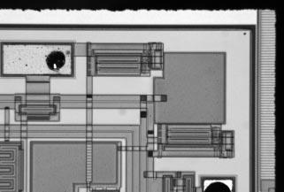
15 INDEX TO FIGURES ASSEMBLY Figures 1-6 DIE LAYOUT AND IDENTIFICATION Figures 7-9 PHYSICAL DIE STRUCTURES Figures COLOR DRAWING OF DIE STRUCTURE Figure 27 CAPACITORS AND RESISTORS Figures CIRCUIT LAYOUT AND I/O Figures ii -

16 Figure 1. Package photographs of the Rockwell R Mag. 4.5x.
17 PIN 1 Figure 2. X-ray view of the package. Mag. 4.5x. PIN 1 Si IC GaAs IC Figure 3. Optical view illustrating decapsulated package. Mag. 4.5x.


18 Au Mag. 620x LEADFRAME Au Mag. 480x BOND PAD Au EDGE OF PASSIVATION Mag. 1600x Figure 4. SEM views of typical wirebonding. 60.


19 DIE PADDLE Mag. 120x EDGE OF PASSIVATION Mag. 1100x Figure 5. SEM views illustrating dicing and edge seal. 60


20 EDGE OF PASSIVATION DIE Mag. 800x METAL 2 EDGE OF PASSIVATION METAL 1 N+ Mag. 6500x Figure 6. SEM section views of the edge seal.

21 Figure 7. Whole die photograph of the Silicon IC. Mag. 45x.


22 Mag. 150x Mag. 300x Figure 8. Optical views of die markings.


23 Figure 9. Optical views of die corners. Mag. 100x.


24 METAL 2 SOG PASSIVATION 2 METAL 1 POLY GATE LOCOS P+ S/D METAL 1 PASSIVATION 2 SOG Ti SILICIDE LOCOS POLY GATE glass etch Figure 10. SEM section views illustrating general structure. Mag. 13,000x.


25 Mag. 3700x Mag. 20,000x Figure 11. SEM views illustrating final passivation. 60.


26 PASSIVATION 2 METAL 2 ILD Mag. 13,000x PASSIVATION 2 TiN CAP PASSIVATION 1 ALUMINUM 2 TiN BARRIER Mag. 26,000x Figure 12. SEM section views of metal 2 line profiles.


27 METAL 2 VIAS Figure 13. Topological SEM views of metal 2 patterning. Mag. 1600x, 0.


28 Mag. 2000x Mag. 2700x TiN CAP Mag. 22,000x ALUMINUM Figure 14. Perspective SEM views of metal 2 step coverage. 60.


29 VOIDS METAL 2 Mag. 13,000x METAL 1 TiN CAP METAL 2 Mag. 52,000x ALUMINUM 1 TiN BARRIER ILD Mag. 40,000x METAL 1 SOG Figure 15. SEM section views illustrating typical vias and interlevel dielectric composition.


30 METAL 2 100% THINNING VOID Mag. 26,000x METAL 1 METAL 2 SOG Mag. 26,000x METAL 1 OVERETCH GAP IN METAL 2 Mag. 52,000x METAL 1 OVERETCH Figure 16. SEM section views of via defects.


31 PASSIVATION 2 METAL 1 PRE-METAL DIELECTRIC Mag. 20,000x TiN CAP SOG ILD ALUMINUM 1 TiN BARRIER Mag. 26,000x Figure 17. SEM section views of metal 1 line profiles.


32 Mag. 1600x Mag. 1600x METAL 1 VIA Mag. 3200x CONTACTS Figure 18. Topological SEM views of metal 1 patterning. 0.


33 Mag. 4000x Mag. 4000x TiN CAP Mag. 27,000x ALUMINUM 1 TiN BARRIER Figure 19. Perspective SEM views of metal 1 step coverage. 60.


34 SOG METAL 1 POLY 1 LOCOS METAL 1 PRE-METAL DIELECTRIC N+ SOG ILD METAL 1 P+ Figure 20. SEM section views of typical metal 1 contacts. Mag. 26,000x.


35 METAL 1 ILD SOG SOG Ti SILICIDE 100% THINNING LOCOS POLY GATE Ti SILICIDE Mag. 26,000x SOG METAL 1 Ti SILICIDE Mag. 52,000x Figure 21. SEM section views of a typical metal 1 contact. Glass etch.


36 Figure 22. Topological SEM views of poly patterning. Mag. 1600x, 0.


37 Mag. 4000x Mag. 4000x POLY GATE Mag. 28,000x S/D LOCOS Figure 23. Perspective SEM views of poly coverage. 60.


38 POLY 1 GATE N-channel N+ S/D N+ S/D GATE OXIDE SIDEWALL SPACER POLY 1 GATE P-channel P+ S/D P + S/D GATE OXIDE Ti SILICIDE glass etch Ti SILICIDE POLY 1 Figure 24. SEM section views of typical transistors. Mag. 52,000x.


39 POLY 1 LOCOS GATE OXIDE Mag. 52,000x METAL 1 DIFFUSION LOCOS Mag. 26,000x Figure 25. SEM section views of a typical birdsbeak and local oxide isolation.


40 P-WELL Rockwell R N-WELL N-WELL P-EPI P-WELL P-SUBSTRATE Mag. 1240x METAL 1 N+ P-WELL Mag. 13,000x STEP AT WELL BOUNDARY Figure 26. Section views illustrating well structure.
41 Ti SILICIDE TiN CAP TiN BARRIER TiN CAP TiN BARRIER Rockwell R Ti SILICIDE SOG (ILD2) ILD1 NITRIDE PASSIVATION GLASS PASSIVATION ALUMINUM 2 ILD3,,,,,,,,,,,,,,,,,,, ALUMINUM 1 PRE-METAL DIELECTRIC,,,,,,,,,,,,,,,,,,,,,,,,,,,,,,,,,,,,,,,,,,,,,,,, LOCOS POLY 1 P+ S/D N-WELL,,,,,,,,,, P-EPI P SUBSTRATE N+ S/D Orange = Nitride, Blue = Metal, Yellow = Oxide, Green = Poly, Red = Diffusion, and Gray = Substrate Figure 27. Color cross section drawing illustrating device structure. P-WELL


42 DIFFUSED RESISTOR CAPACITOR POLY 1 RESISTOR Figure 28. Optical views of resistors and a capacitor. Mag. 600x.


43 PATTERNED OXIDE (MASK) SOG METAL 1 LOCOS Mag. 26,000x DENSIFIED OXIDE POLY 1 RESISTOR LOCOS Mag. 52,000x Figure 29. SEM section views of a poly 1 resistor.


44 PASSIVATION 2 METAL 1 LOCOS POLY 1 Mag. 13,000x METAL 1 POLY 1 CAPACITOR DIELECTRIC LOCOS Mag. 52,000x Figure 30. SEM section views illustrating a capacitor.


45 intact unlayered Figure 31. Optical views of typical device circuit layout. Mag. 600x.


46 intact unlayered Figure 32. Optical views of typical input protection. Mag. 300x.

47 N+ METAL 1 Figure 33. SEM section view of the I/O circuitry. Mag. 6500x. PASSIVATION 2 METAL 2 ILD N+
Motorola MPA1016FN FPGA
 Construction Analysis Motorola MPA1016FN FPGA Report Number: SCA 9711-561 Global Semiconductor Industry the Serving Since 1964 17350 N. Hartford Drive Scottsdale, AZ 85255 Phone: 602-515-9780 Fax: 602-515-9781
UMC UM F-7 2M-Bit SRAM
 Construction Analysis UMC UM 613264F-7 2M-Bit SRAM Report Number: SCA 9609-511 Global Semiconductor Industry the Serving Since 1964 15022 N. 75th Street Scottsdale, AZ 85260-2476 Phone: 602-998-9780 Fax:
NKK NR4645LQF Bit RISC Microprocessor
 Construction Analysis NKK NR4645LQF-133 64-Bit RISC Microprocessor Report Number: SCA 9707-547 Global Semiconductor Industry the Serving Since 1964 17350 N. Hartford Drive Scottsdale, AZ 85255 Phone: 602-515-9870
Lattice isplsi1032e CPLD
 Construction Analysis Lattice isplsi1032e CPLD Report Number: SCA 9612-522 Global Semiconductor Industry the Serving Since 1964 15022 N. 75th Street Scottsdale, AZ 85260-2476 Phone: 602-998-9780 Fax: 602-948-1925
Analog Devices ADSP KS-160 SHARC Digital Signal Processor
 Construction Analysis Analog Devices ADSP-21062-KS-160 SHARC Digital Signal Processor Report Number: SCA 9712-575 Global Semiconductor Industry the Serving Since 1964 17350 N. Hartford Drive Scottsdale,
Mosel Vitelic MS62256CLL-70PC 256Kbit SRAM
 Construction Analysis Mosel Vitelic MS62256CLL-70PC 256Kbit SRAM Report Number: SCA 9703-499 Global Semiconductor Industry the Serving Since 1964 17350 N. Hartford Drive Scottsdale, AZ 85255 Phone: 602-515-9780
Motorola MC68360EM25VC Communication Controller
 Construction Analysis EM25VC Communication Controller Report Number: SCA 9711-562 Global Semiconductor Industry the Serving Since 1964 17350 N. Hartford Drive Scottsdale, AZ 85255 Phone: 602-515-9780 Fax:
SGS-Thomson M28C K EEPROM
 Construction Analysis SGS-Thomson M28C64-121 64K EEPROM Report Number: SCA 9710-559 Global Semiconductor Industry the Serving Since 1964 17350 N. Hartford Drive Scottsdale, AZ 85255 Phone: 602-515-9780
Maximum MAX662 12V DC-DC Converter
 Construction Analysis Maximum MAX662 12V DC-DC Converter Report Number: SCA 9512-445 Global Semiconductor Industry the Serving Since 1964 17350 N. Hartford Drive Scottsdale, AZ 85255 Phone: 602-515-9780
Oki M A-60J 16Mbit DRAM (EDO)
") Construction Analysis Oki M5117805A-60J 16Mbit DRAM (EDO) Report Number: SCA 9707-545 Global Semiconductor Industry the Serving Since 1964 17350 N. Hartford Drive Scottsdale, AZ 85255 Phone: 602-515-9780
Construction Analysis Oki M5117805A-60J 16Mbit DRAM (EDO) Report Number: SCA 9707-545 Global Semiconductor Industry the Serving Since 1964 17350 N. Hartford Drive Scottsdale, AZ 85255 Phone: 602-515-9780
Dallas Semicoductor DS80C320 Microcontroller
 Construction Analysis Dallas Semicoductor DS80C320 Microcontroller Report Number: SCA 9702-525 Global Semiconductor Industry the Serving Since 1964 15022 N. 75th Street Scottsdale, AZ 85260-2476 Phone:
SGS-Thomson L4990 Controller
 Construction Analysis SGS-Thomson L4990 Controller Report Number: SCA 9710-560 Global Semiconductor Industry the Serving Since 1964 17350 N. Hartford Drive Scottsdale, AZ 85255 Phone: 602-515-9780 Fax:
Micron Semiconductor MT5C64K16A1DJ 64K x 16 SRAM
 Construction Analysis Micron Semiconductor MT5C64K16A1DJ 64K x 16 SRAM Report Number: SCA 9412-394 Global Semiconductor Industry the Serving Since 1964 17350 N. Hartford Drive Scottsdale, AZ 85255 Phone:
Lattice 3256A-90LM PLD
 Construction Analysis PLD Report Number: SCA 9705-538 Global Semiconductor Industry the Serving Since 1964 17350 N. Hartford Drive Scottsdale, AZ 85255 Phone: 602-515-9780 Fax: 602-515-9781 e-mail: ice@ice-corp.com
DEC SA-110S StrongARM 32-Bit Microprocessor
 Construction Analysis DEC SA-110S StrongARM 32-Bit Microprocessor Report Number: SCA 9704-535 Global Semiconductor Industry the Serving Since 1964 15022 N. 75th Street Scottsdale, AZ 85260-2476 Phone:
National Semiconductor LM2672 Simple Switcher Voltage Regulator
 Construction Analysis National Semiconductor LM2672 Simple Switcher Voltage Regulator Report Number: SCA 9712-570 Global Semiconductor Industry the Serving Since 1964 17350 N. Hartford Drive Scottsdale,
NEC 79VR5000 RISC Microprocessor
 Construction Analysis NEC 79VR5000 RISC Microprocessor Report Number: SCA 9711-567 Global Semiconductor Industry the Serving Since 1964 17350 N. Hartford Drive Scottsdale, AZ 85255 Phone: 602-515-9780
Hitachi A 64Mbit (8Mb x 8) Dynamic RAM
 Dynamic RAM") Construction Analysis Hitachi 5165805A 64Mbit (8Mb x 8) Dynamic RAM Report Number: SCA 9712-565 Global Semiconductor Industry the Serving Since 1964 17350 N. Hartford Drive Scottsdale, AZ 85255 Phone:
Construction Analysis Hitachi 5165805A 64Mbit (8Mb x 8) Dynamic RAM Report Number: SCA 9712-565 Global Semiconductor Industry the Serving Since 1964 17350 N. Hartford Drive Scottsdale, AZ 85255 Phone:
Micron Semiconductor MT4LC16M4H9 64Mbit DRAM
 Construction Analysis Micron Semiconductor MT4LC16M4H9 64Mbit DRAM Report Number: SCA 9705-539 Global Semiconductor Industry the Serving Since 1964 15022 N. 75th Street Scottsdale, AZ 85260-2476 Phone:
Xilinx XC4036XL-1C FPGA
 Construction Analysis Xilinx XC4036XL-1C FPGA Report Number: SCA 9709-553 Global Semiconductor Industry the Serving Since 1964 17350 N. Hartford Drive Scottsdale, AZ 85255 Phone: 602-515-9780 Fax: 602-515-9781
Altera EPM7128SQC EPLD
 Construction Analysis Altera EPM7128SQC160-15 EPLD Report Number: SCA 9712-569 Global Semiconductor Industry the Serving Since 1964 17350 N. Hartford Drive Scottsdale, AZ 85255 Phone: 602-515-9780 Fax:
Xilinx XC4036EX FPGA
 Construction Analysis Xilinx XC4036EX FPGA Report Number: SCA 9706-544 Global Semiconductor Industry the Serving Since 1964 15022 N. 75th Street Scottsdale, AZ 85260-2476 Phone: 602-998-9780 Fax: 602-948-1925
SGS-Thomson M17C1001 1Mb UVEPROM
 Construction Analysis SGS-Thomson M17C1001 1Mb UVEPROM Report Number: SCA 9612-518 Global Semiconductor Industry the Serving Since 1964 15022 N. 75th Street Scottsdale, AZ 85260-2476 Phone: 602-998-9780
VTC VM365830VSJ Pre-Amp
 Construction Analysis VTC VM365830VSJ Pre-Amp Report Number: SCA 9708-549 Global Semiconductor Industry the Serving Since 1964 17350 N. Hartford Drive Scottsdale, AZ 85255 Phone: 602-515-9780 Fax: 602-515-9781
Motorola PC603R Microprocessor
 Construction Analysis Motorola PC603R Microprocessor Report Number: SCA 9709-551 Global Semiconductor Industry the Serving Since 1964 17350 N. Hartford Drive Scottsdale, AZ 85255 Phone: 602-515-9780 Fax:
Intel Pentium Processor W/MMX
 Construction Analysis Intel Pentium Processor W/MMX Report Number: SCA 9706-540 Global Semiconductor Industry the Serving Since 1964 15022 N. 75th Street Scottsdale, AZ 85260-2476 Phone: 602-998-9780 Fax:
Integrated Circuit Engineering Corporation. DRAMs
 DRAMs As generally known, the focus of technology in this product category continues to be complex vertical polysilicon structures to reduce cell area. This not only pushes the limits of deposition and
Integrated Circuit Engineering Corporation EPROM
 EPROM There was lots of discussion and many technical papers covering the promises of EPROM (typically Flash) at the IEDM conference last December, but here as in the other memory areas, not much in the
Renesas M5M40R326 32Mbit DRAM Memory Structural Analysis
 August 13, 2004 Renesas M5M40R326 32Mbit DRAM Memory Structural Analysis For questions, comments, or more information about this report, or for any additional technical needs concerning semiconductor technology,
Lecture 030 Integrated Circuit Technology - I (5/8/03) Page 030-1
 Page 030-1") Lecture 030 Integrated Circuit Technology - I (5/8/03) Page 030-1 LECTURE 030 INTEGRATED CIRCUIT TECHNOLOGY - I (References [7,8]) Objective The objective of this presentation is: 1.) Illustrate integrated
Lecture 030 Integrated Circuit Technology - I (5/8/03) Page 030-1 LECTURE 030 INTEGRATED CIRCUIT TECHNOLOGY - I (References [7,8]) Objective The objective of this presentation is: 1.) Illustrate integrated
9/4/2008 GMU, ECE 680 Physical VLSI Design
 ECE680: Physical VLSI Design Chapter II CMOS Manufacturing Process 1 Dual-Well Trench-Isolated CMOS Process gate-oxide TiSi 2 AlCu Tungsten SiO 2 p-well poly n-well SiO 2 n+ p-epi p+ p+ 2 Schematic Layout
Chapter 2 Manufacturing Process
 Digital Integrated Circuits A Design Perspective Chapter 2 Manufacturing Process 1 CMOS Process 2 CMOS Process (n-well) Both NMOS and PMOS must be built in the same silicon material. PMOS in n-well NMOS
Chapter 4 : ULSI Process Integration (0.18 m CMOS Process)
") Chapter : ULSI Process Integration (0.8 m CMOS Process) Reference. Semiconductor Manufacturing Technology : Michael Quirk and Julian Serda (00). - (00). Semiconductor Physics and Devices- Basic Principles(/e)
Chapter : ULSI Process Integration (0.8 m CMOS Process) Reference. Semiconductor Manufacturing Technology : Michael Quirk and Julian Serda (00). - (00). Semiconductor Physics and Devices- Basic Principles(/e)
Manufacturing Process
 Digital Integrated Circuits A Design Perspective Jan M. Rabaey Anantha Chandrakasan Borivoje Nikolic Manufacturing Process July 30, 2002 1 CMOS Process 2 A Modern CMOS Process gate-oxide TiSi 2 AlCu Tungsten
CMOS Technology. Flow varies with process types & company. Start with substrate selection. N-Well CMOS Twin-Well CMOS STI
 CMOS Technology Flow varies with process types & company N-Well CMOS Twin-Well CMOS STI Start with substrate selection Type: n or p Doping level, resistivity Orientation, 100, or 101, etc Other parameters
ECE 659. Jan M. Rabaey Anantha Chandrakasan Borivoje Nikolic. July 30, Digital EE141 Integrated Circuits 2nd Manufacturing.
 Digital Integrated Circuits A Design Perspective Jan M. Rabaey Anantha Chandrakasan Borivoje Nikolic Manufacturing Process July 0, 00 1 CMOS Process 1 A Modern CMOS Process gate-oxide TiSi AlCu Tungsten
Manufacturing Process
 CMOS Manufacturing Process CMOS Process 1 A Modern CMOS Process gate-oxide TiSi AlCu Tungsten SiO n+ p-well p-epi poly n-well p+ SiO p+ Dual-Well Trench-Isolated CMOS Process Circuit Under Design V DD
CMOS Manufacturing Process
 CMOS Manufacturing Process CMOS Process A Modern CMOS Process gate-oxide TiSi 2 AlCu Tungsten SiO 2 n+ p-well p-epi poly n-well p+ SiO 2 p+ Dual-Well Trench-Isolated CMOS Process Circuit Under Design V
ECE520 VLSI Design. Lecture 7: CMOS Manufacturing Process. Payman Zarkesh-Ha
 ECE520 VLSI Design Lecture 7: CMOS Manufacturing Process Payman Zarkesh-Ha Office: ECE Bldg. 230B Office hours: Wednesday 2:00-3:00PM or by appointment E-mail: pzarkesh@unm.edu Slide: 1 Review of Last
EE 434 Lecture 9. IC Fabrication Technology
 EE 434 Lecture 9 IC Fabrication Technology Quiz 7 The layout of a film resistor with electrodes A and B is shown. If the sheet resistance of the film is 40 /, determine the resistance between nodes A and
ECE321 Electronics I
 ECE321 Electronics I Lecture 19: CMOS Fabrication Payman Zarkesh-Ha Office: ECE Bldg. 230B Office hours: Tuesday 2:00-3:00PM or by appointment E-mail: payman@ece.unm.edu Slide: 1 Miller Effect Interconnect
EE 330 Lecture 9. IC Fabrication Technology Part II. -Oxidation -Epitaxy -Polysilicon -Planarization -Resistance and Capacitance in Interconnects
 EE 330 Lecture 9 IC Fabrication Technology Part II -Oxidation -Epitaxy -Polysilicon -Planarization -Resistance and Capacitance in Interconnects Review from Last Time Etching Dry etch (anisotropic) SiO
10 Manor Parkway, Suite C Salem, New Hampshire
 Micro-Precision Technologies (MPT) is an independent manufacturer of hybrid integrated circuits, multichip modules, and high-precision thick film substrates for the military, medical, avionics, optoelectronics,
EE 560 FABRICATION OF MOS CIRCUITS. Kenneth R. Laker, University of Pennsylvania
 1 EE 560 FABRICATION OF MOS CIRCUITS 2 CMOS CHIP MANUFACTRING STEPS Substrate Wafer Wafer Fabrication (diffusion, oxidation, photomasking, ion implantation, thin film deposition, etc.) Finished Wafer Wafer
EE 330 Lecture 9. IC Fabrication Technology Part 2
 EE 330 Lecture 9 IC Fabrication Technology Part 2 Quiz 8 A 2m silicon crystal is cut into wafers using a wire saw. If the wire diameter is 220um and the wafer thickness is 350um, how many wafers will this
Chapter 4 Fabrication Process of Silicon Carrier and. Gold-Gold Thermocompression Bonding
 Chapter 4 Fabrication Process of Silicon Carrier and Gold-Gold Thermocompression Bonding 4.1 Introduction As mentioned in chapter 2, the MEMs carrier is designed to integrate the micro-machined inductor
Silicon Epitaxial CVD Want to create very sharp PN boundary grow one type layer on other in single crystal form High dopant layers on low dopant
 Silicon Epitaxial CVD Want to create very sharp PN boundary grow one type layer on other in single crystal form High dopant layers on low dopant substrate Creates latch up protection for CMOS Buried Epi
We are moving to 155 Donner Lab From Thursday, Feb 2 We will be able to accommodate everyone!
 -Spring 006 Digital Integrated Circuits Lecture 4 CMOS Manufacturing Process Design Rules EECS141 1 Good News! We are moving to 155 Donner Lab From Thursday, Feb We will be able to accommodate everyone!
Semiconductor Manufacturing Technology. IC Fabrication Process Overview
 Semiconductor Manufacturing Technology Michael Quirk & Julian Serda October 00 by Prentice Hall Chapter 9 IC Fabrication Process Overview /4 Objectives After studying the material in this chapter, you
Packaging and Ball Bonding Gold wire makes contact from bonding pads on chip to package Gold wire is formed into ball to make contact Uses an
 Packaging and Ball Bonding Gold wire makes contact from bonding pads on chip to package Gold wire is formed into ball to make contact Uses an ultrasonic process & heat Process called "Ball Bonding" Wedge
Silicon Epitaxial CVD Want to create very sharp PN boundary grow one type layer on other in single crystal form High dopant layers on low dopant
 Silicon Epitaxial CVD Want to create very sharp PN boundary grow one type layer on other in single crystal form High dopant layers on low dopant substrate Creates latch up protection for CMOS Buried Epi
Lecture 1A: Manufacturing& Layout
 Introduction to CMOS VLSI Design Lecture 1A: Manufacturing& Layout David Harris Harvey Mudd College Spring 2004 Steven Levitan Fall 2008 1 The Manufacturing Process For a great tour through the IC manufacturing
Manufacturing Process
 Manufacturing Process 1 CMOS Process 2 A Modern CMOS Process gate-oxide TiSi 2 AlCu Tungsten SiO 2 n+ p-well p-epi poly n-well p+ SiO 2 p+ Dual-Well Trench-Isolated CMOS Process 3 Single-crystal ingot
Lecture 200 BiCMOS Technology (12/12/01) Page 200-1
 Page 200-1") Lecture 200 BiCMOS Technology (12/12/01) Page 200-1 LECTURE 200 BICMOS TECHNOLOGY (READING: Text-Sec. 2.11) INTRODUCTION Objective Illustrate BiCMOS technology Outline Introduction Physical process illustration
Lecture 200 BiCMOS Technology (12/12/01) Page 200-1 LECTURE 200 BICMOS TECHNOLOGY (READING: Text-Sec. 2.11) INTRODUCTION Objective Illustrate BiCMOS technology Outline Introduction Physical process illustration
Chapter 3 Silicon Device Fabrication Technology
 Chapter 3 Silicon Device Fabrication Technology Over 10 15 transistors (or 100,000 for every person in the world) are manufactured every year. VLSI (Very Large Scale Integration) ULSI (Ultra Large Scale
EE BACKEND TECHNOLOGY - Chapter 11. Introduction
 1 EE 212 FALL 1999-00 BACKEND TECHNOLOGY - Chapter 11 Introduction Backend technology: fabrication of interconnects and the dielectrics that electrically and physically separate them. Aluminum N+ Early
Fabrication and Layout
 Fabrication and Layout Kenneth Yun UC San Diego Adapted from EE271 notes, Stanford University Overview Semiconductor properties How chips are made Design rules for layout Reading Fabrication: W&E 3.1,
EE 330 Lecture 9. IC Fabrication Technology Part II. -Oxidation -Epitaxy -Polysilicon -Planarization -Resistance and Capacitance in Interconnects
 EE 330 Lecture 9 IC Fabrication Technology Part II -Oxidation -Epitaxy -Polysilicon -Planarization -Resistance and Capacitance in Interconnects Review from Last Time IC Fabrication Technology Crystal Preparation
VLSI Design and Simulation
 VLSI Design and Simulation CMOS Processing Technology Topics CMOS Processing Technology Semiconductor Processing How do we make a transistor? Fabrication Process Wafer Processing Silicon single crystal
CS/ECE 5710/6710. N-type Transistor. N-type from the top. Diffusion Mask. Polysilicon Mask. CMOS Processing
 CS/ECE 5710/6710 CMOS Processing Addison-Wesley N-type Transistor D G +Vgs + Vds S N-type from the top i electrons - Diffusion Mask Mask for just the diffused regions Top view shows patterns that make
UT Austin, ECE Department VLSI Design 2. CMOS Fabrication, Layout Rules
 2. CMOS Fabrication, Layout, Design Rules Last module: Introduction to the course How a transistor works CMOS transistors This module: CMOS Fabrication Design Rules CMOS Fabrication CMOS transistors are
Microelectronics. Integrated circuits. Introduction to the IC technology M.Rencz 11 September, Expected decrease in line width
 Microelectronics Introduction to the IC technology M.Rencz 11 September, 2002 9/16/02 1/37 Integrated circuits Development is controlled by the roadmaps. Self-fulfilling predictions for the tendencies
Destructive Physical Analysis (DPA) Program Methodology
 Program Methodology") Destructive Physical Analysis (DPA) Program Methodology DPA: Introduction Destructive Physical Analysis (DPA) is a comprehensive quality assessment for workmanship on Printed Circuit Board Assemblies (PCBAs).
Destructive Physical Analysis (DPA) Program Methodology DPA: Introduction Destructive Physical Analysis (DPA) is a comprehensive quality assessment for workmanship on Printed Circuit Board Assemblies (PCBAs).
Quality and Reliability Report
 Quality and Reliability Report Product Qualification MASW-007921 2mm 8-Lead Plastic Package QTR-0148 M/A-COM Technology Solutions Inc. 100 Chelmsford Street Lowell, MA 01851 Tel: (978) 656-2500 Fax: (978)
Fabrication and Layout
 ECEN454 Digital Integrated Circuit Design Fabrication and Layout ECEN 454 3.1 A Glimpse at MOS Device Polysilicon Aluminum ECEN 475 4.2 1 Material Classification Insulators Glass, diamond, silicon oxide
Process Integration. MEMS Release Techniques Sacrificial Layer Removal Substrate Undercut
 Process Integration Self-aligned Techniques LOCOS- self-aligned channel stop Self-aligned Source/Drain Lightly Doped Drain (LDD) Self-aligned silicide (SALICIDE) Self-aligned oxide gap MEMS Release Techniques
1 Thin-film applications to microelectronic technology
 1 Thin-film applications to microelectronic technology 1.1 Introduction Layered thin-film structures are used in microelectronic, opto-electronic, flat panel display, and electronic packaging technologies.
Quality and Reliability Report
 Quality and Reliability Report Product Qualification MAAM-008819 2mm 8-Lead PDFN Plastic Package QTR-0147 M/A-COM Technology Solutions Inc. 100 Chelmsford Street Lowell, MA 01851 Tel: (978) 656-2500 Fax:
IMPACT OF MICROVIA-IN-PAD DESIGN ON VOID FORMATION
 IMPACT OF MICROVIA-IN-PAD DESIGN ON VOID FORMATION Frank Grano, Felix Bruno Huntsville, AL Dana Korf, Eamon O Keeffe San Jose, CA Cheryl Kelley Salem, NH Joint Paper by Sanmina-SCI Corporation EMS, GTS
CMOS Processing Technology
 CHAPTER 2 CMOS Processing Technology Outline 2 1. CMOS Technologies 2. Layout Design Rules 3. CMOS Process Enhancements 4. Technology-related CAD Issues 5. Manufacturing Issues CMOS Technologies 3 n-well
Oxidation SMT Yau - 1
 Oxidation Yau - 1 Objectives After studying the material in this chapter, you will be able to: 1. Describe an oxide film for semiconductor manufacturing, including its atomic structure, how it is used
CMOS Processing Technology
 CHAPTER 2 CMOS Processing Technology Outline 2 1. CMOS Technologies 2. Layout Design Rules 3. CMOS Process Enhancements 4. Technology-related CAD Issues 5. Manufacturing Issues CMOS Technologies 3 n-well
ASIM-X MEMS-Specific Design Rules
 ASIM-X MEMS-Specific Design Rules Version 2 Revised April 5, 2006. This is a beta version, subject to change. Revised by G. K. Fedder, Carnegie Mellon University. 1 Process Overview ASIM-X, an acronym
CMOS Manufacturing process. Design rule set
 CMOS Manufacturing process Circuit design Set of optical masks Fabrication process Circuit designer Design rule set Process engineer All material: Chap. 2 of J. Rabaey, A. Chandrakasan, B. Nikolic, Digital
ECSE 6300 IC Fabrication Laboratory Lecture 8 Metallization. Die Image
 ECSE 6300 IC Fabrication Laboratory Lecture 8 Metallization Prof. Rensselaer Polytechnic Institute Troy, NY 12180 Office: CII-6229 Tel.: (518) 276-2909 e-mails: luj@rpi.edu http://www.ecse.rpi.edu/courses/s18/ecse
Silicon Wafer Processing PAKAGING AND TEST
 Silicon Wafer Processing PAKAGING AND TEST Parametrical test using test structures regularly distributed in the wafer Wafer die test marking defective dies dies separation die fixing (not marked as defective)
CMOS FABRICATION. n WELL PROCESS
 CMOS FABRICATION n WELL PROCESS Step 1: Si Substrate Start with p- type substrate p substrate Step 2: Oxidation Exposing to high-purity oxygen and hydrogen at approx. 1000 o C in oxidation furnace SiO
Chapter 5 Thermal Processes
 Chapter 5 Thermal Processes 1 Topics Introduction Hardware Oxidation Diffusion Annealing Post-Implantation Alloying Reflow High Temp CVD Epi Poly Silicon Nitride RTP RTA RTP Future Trends 2 Definition
Chapter 3 CMOS processing technology
 Chapter 3 CMOS processing technology (How to make a CMOS?) Si + impurity acceptors(p-type) donors (n-type) p-type + n-type => pn junction (I-V) 3.1.1 (Wafer) Wafer = A disk of silicon (0.25 mm - 1 mm thick),
EE CMOS TECHNOLOGY- Chapter 2 in the Text
 1 EE 212 FALL 1999-00 CMOS TECHOLOGY- Chapter 2 in the Text In this set of notes we will describe a modern CMOS process flow. In the simplest CMOS technologies, we need to realize simply MOS and MOS transistors
Process Integration. NMOS Generic NMOS Process Flow. CMOS - The MOSIS Process Flow
 Process Integration Self-aligned Techniques LOCOS- self-aligned channel stop Self-aligned Source/Drain Lightly Doped Drain (LDD) Self-aligned silicide (SALICIDE) Self-aligned oxide gap MEMS Release Techniques
IC Fabrication Technology Part III Devices in Semiconductor Processes
 EE 330 Lecture 10 IC Fabrication Technology Part III Metalization and Interconnects Parasitic Capacitances Back-end Processes Devices in Semiconductor Processes Resistors Diodes Review from Last Lecture
Czochralski Crystal Growth
 Czochralski Crystal Growth Crystal Pulling Crystal Ingots Shaping and Polishing 300 mm wafer 1 2 Advantage of larger diameter wafers Wafer area larger Chip area larger 3 4 Large-Diameter Wafer Handling
Cost of Integrated Circuits
 Cost of IC Design 1 Cost of Integrated Circuits NRE (Non-Recurrent Engineering) costs fixed design time and effort, mask generation independent of sales volume / number of products one-time cost factor
Nonplanar Metallization. Planar Metallization. Professor N Cheung, U.C. Berkeley
 Nonplanar Metallization Planar Metallization Passivation Metal 5 (copper) Metal 3 (copper) Interlevel dielectric (ILD) Via (tungsten) Metal 1 (copper) Tungsten Plug to Si Silicon Caps and Plugs oxide oxide
MIL-STD-883H METHOD INTERNAL VISUAL (MONOLITHIC)
") * INTERNAL VISUAL (MONOLITHIC) 1. PURPOSE. The purpose of this test is to check the internal materials, construction, and workmanship of microcircuits for compliance with the requirements of the applicable
* INTERNAL VISUAL (MONOLITHIC) 1. PURPOSE. The purpose of this test is to check the internal materials, construction, and workmanship of microcircuits for compliance with the requirements of the applicable
Isolation Technology. Dr. Lynn Fuller
 ROCHESTER INSTITUTE OF TECHNOLOGY MICROELECTRONIC ENGINEERING Isolation Technology Dr. Lynn Fuller Motorola Professor 82 Lomb Memorial Drive Rochester, NY 14623-5604 Tel (585) 475-2035 Fax (585) 475-5041
Interconnects OUTLINE
 Interconnects 1 Interconnects OUTLINE 1. Overview of Metallization 2. Introduction to Deposition Methods 3. Interconnect Technology 4. Contact Technology 5. Refractory Metals and their Silicides Reading:
Failure Modes in Wire bonded and Flip Chip Packages
 Failure Modes in Wire bonded and Flip Chip Packages Mumtaz Y. Bora Peregrine Semiconductor San Diego, Ca. 92121 mbora@psemi.com Abstract The growth of portable and wireless products is driving the miniaturization
EE 143 CMOS Process Flow
 EE 143 CMOS rocess Flow CT 84 D D G Sub G Sub S S G D S G D S + + + + - MOS Substrate Well - MOS Substrate EE 143 CMOS rocess Flow CT 85 hotoresist Si 3 4 SiO 2 Substrate selection: moderately high resistivity,
Beam Leads. Spider bonding, a precursor of TAB with all-metal tape
 Beam Leads The vast majority of chips are intended for connection with thermosonic bonds: all other methods require some modification to the wafer. As early as 1972, Jordan described three gang-bonding
CHAPTER - 4 CMOS PROCESSING TECHNOLOGY
 CHAPTER - 4 CMOS PROCESSING TECHNOLOGY Samir kamal Spring 2018 4.1 CHAPTER OBJECTIVES 1. Introduce the CMOS designer to the technology that is responsible for the semiconductor devices that might be designed
CX Thin Fil s. Resistors Attenuators Thin-Film Products Thin-Film Services. ISO 9001:2008 RoHS/REACH Compliant ITAR Compliant
 CX Thin Fil s Resistors Attenuators Thin-Film Products Thin-Film Services www.cxthinfilms.com ISO 9001:2008 RoHS/REACH Compliant ITAR Compliant www.cxthinfilms.com sales@cxthinfilms.com +1 (401) 461-5500
Semiconductor Manufacturing Technology. Semiconductor Manufacturing Technology
 Semiconductor Manufacturing Technology Michael Quirk & Julian Serda October 2001 by Prentice Hall Chapter 10 Oxidation 2001 2000 by Prentice Hall Diffusion Area of Wafer Fabrication Wafer fabrication (front-end)
Abstract. Key words. I. Introduction
 Increased High-Temperature Reliability and Package Hardening of Commercial Integrated Circuits (Through Die Extraction, Electroless Nickel/Gold Pad Reconditioning, and Ceramic Re-Assembly) Erick M. Spory
INTEGRATED-CIRCUIT TECHNOLOGY
 INTEGRATED-CIRCUIT TECHNOLOGY 0. Silicon crystal growth and wafer preparation 1. Processing Steps 1.1. Photolitography 1.2. Oxidation 1.3. Layer Deposition 1.4. Etching 1.5. Diffusion 1.6 Backend: assembly,
Innovative MID Plating Solutions
 Innovative MID Plating Solutions High Reliability Wire Bond Technique for MIDs Jordan Kologe MacDermid Electronics Solutions jkologe@macdermid.com 1 MacDermid: Specialty Chemical Solutions Over 2000 Worldwide
Lecture 2. Fabrication and Layout
 Lecture 2 Fabrication and Layout Mark Horowitz Modified by Azita Emami Computer Systems Laboratory Stanford University azita@stanford.edu 1 Overview Reading W&E 3.1(scan), 3.2.1, 3.3.1 - Fabrication W&E
PROCESS FLOW AN INSIGHT INTO CMOS FABRICATION PROCESS
 Contents: VI Sem ECE 06EC63: Analog and Mixed Mode VLSI Design PROCESS FLOW AN INSIGHT INTO CMOS FABRICATION PROCESS 1. Introduction 2. CMOS Fabrication 3. Simplified View of Fabrication Process 3.1 Alternative
Make sure the exam paper has 9 pages total (including cover page)
") UNIVERSITY OF CALIFORNIA College of Engineering Department of Electrical Engineering and Computer Sciences Fall 2010 EE143 Midterm Exam #2 Family Name First name SID Signature Solution Make sure the exam
UNIVERSITY OF CALIFORNIA College of Engineering Department of Electrical Engineering and Computer Sciences Fall 2010 EE143 Midterm Exam #2 Family Name First name SID Signature Solution Make sure the exam