Laser Micromachining for Industrial Applications and R&D. 3D-Micromac AG. Symposium on Smart Integrated Systems in Chemnitz. 3D-Micromac AG
|
|
|
- Lynette Goodman
- 6 years ago
- Views:
Transcription
1 3D-Micromac AG Symposium on Smart Integrated Systems in Chemnitz 1
2 1 microdice - TLS-Dicing for separation of SiC 2 microprep - for high-throughput microstructure diagnostics 3 About 3D-Micromac AG 2

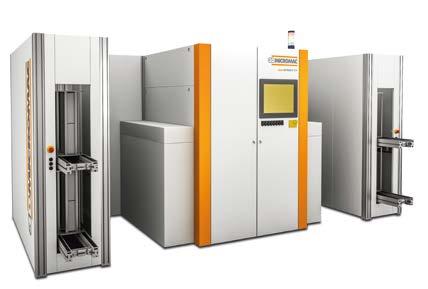
3 microdice system TLS-Dicing for separation of SiC wafers Courtesy of Infineon AG 3

4 Current situation by using dicing saws Cost High costs for saw blades Reduced uptime Quality Delamination of back-side metal Defects by chipping Speed 2-10 mm/s Limited throughput 4


5 Our solution TLS-Dicing with microdice System For excellent cleaving results and higher throughput 5

6 Your advantages using TLS-Dicing technology Cost reduction Minimal CoO due to contactless processing Increased yield by zero kerf Function Back-side metal can be separated without delamination Several wafer editable Speed Dicing speed up to 300 mm/s Higher throughput due the higher process speed 6


7 Advantages at a glance Free of residues Free of chipping Zero kerf Perfect sidewalls 7
8 microdice system Up to 300 mm (12 ) wafer size Integrated laser sources with long lifetime Integrated patented micro stretching function Automated wafer handling SECS / GEM interface Compatible with common SEMI standards Consumables: only DI-water microdice 8

9 Summary Significant cost reduction Higher throughput Increased yield Damage-free back-side metal 9
10 Product roadmap TLS-Dicing 2014 Q1/2014 Q3/2014 Q3/2014 Q4/2014 Q1/ Project Start Tool-Spec / Design Product launch 1 st serial tool Customer evaluatio n Application is possible all time! 1 st / 2 nd / side Semicon West TLS-Dicing TM for additional materials and applications TLS-Dicing with optimized yield 10
11 1 microdice - TLS-Dicing for separation of SiC 2 microprep - for high-throughput microstructure diagnostics 3 About 3D-Micromac AG 11
12 microprep New vistas for targeted and high-throughput microstructure diagnostics 12
13 Transmission Electron Microscopy (TEM) Classical ways Many ways to achieve electron transparency Grind up Ion beam etching Tripod grinding electrontransparent section Electrolytic etching Ultramicrotomy µcleave FIB processing In cooperation with 13

 10 µm FIB")

14 One common way to achieve electron transparency - FIB Lamella preparation with a focused ion beam (FIB) 10 µm FIB is a proven method, but the process is very complex 250 µm In cooperation with 14


15 Expanding the opportunities by using laser Laser processing as a all-new instrument to achieve electron transparency Grind up Laser processing Ion beam etching Tripod grinding electrontransparent section Electrolytic etching Ultramicrotomy µcleave FIB processing In cooperation with 15

16 Laser Properties High power densities Materials ablation Precise local delivery and focusing Just photons clean in terms of contamination Low running costs High fluences non-linear optics: Multi-photon absorption Machining of transparent-at-the-wavelength materials feasible Source: Scanlab Is structural damage an issue? In cooperation with 16

17 Laser Induced Structural Damage? Controllable! Silicon, laser machined with ultrashort pulses Recrystallization along flanks to a depth of 150 nm to 450 nm No significant changes to the bulk material beyond this depth detected (e.g., no dislocations, stacking faults etc.) Depth of the laser kerf > 15 µm Flanks of laser micromachining Recrystallized volume In cooperation with 17
18 Motivation using laser for TEM Very high ablation rates using FIB-technology not achievable Method Milling rate of silicon [µm³/s] Time needed to remove 0.3 mm³ Spot diameter (theory) Structural-damage depth [nm] FIB (Ga + ) High- Current FIB FIB plus GIS Plasma FIB (Xe + ) 355-nm DPSS Laser 2, years 116 days 14 days 1.7 days 5 min ca. 20 nm (@ 100 pa) ca. 200 nm (@ 100 pa) 500 nm 2-20 nm 2-20 nm < 2 4 µm In Parts after: Martens et al., EuroSimE, In cooperation with 18


19 microprep Process Flow Step 1 Step 2 Step 3 Step 4 Step 5 Step 6 Plane-parallel thinning to µm Assembling the plate on a flat mount Laser cutting of the base structure Transferring base structure to a dedicated clamping jig Local laser thinning of preselected areas Final thinning with Ar+ ion broad beam or FIB Preparation step microprep steps Follow-up step In cooperation with 19


20 microprep Process Flow Step1 Step 2 Step 3 Step 4 Step 5 Step 6 Steps 1 & 2 Providing a plane-parallel plate and firmly fixing it to a jig Parts of the jig In cooperation with 20


21 microprep Process Flow Step1 Step 2 Step 3 Step 4 Step 5 Step 6 Step 3 Laser cutting of the supporting base structure Examples of base structures Cutted base structure In cooperation with 21


22 microprep Process Flow Step1 Step 2 Step 3 Step 4 Step 5 Step 6 Step 3 Laser cutting of the supporting base structure As-cut flank in silicon Tomographic basic structure laser-machined into silicon In cooperation with 22


23 microprep Process Flow Step1 Step 2 Step 3 Step 4 Step 5 Step 6 Step 4 Transferring the supporting base structure to a dedicated clamping jig Clamping jig Basic structure fixed by the jig In cooperation with 23

")


24 microprep Process Flow Step1 Step 2 Step 3 Step 4 Step 5 Step 6 Step 5 Local laser thinning of preselected areas (high-throughput screening) Local thinning in a box-like manner Local thinning of multiple probing positions Automated preparation of a pillar array In cooperation with 24


25 microprep Process Flow Step1 Step 2 Step 3 Step 4 Step 5 Step 6 Step 5 Local laser thinning of preselected areas (high-throughput screening) Smooth flanks Local thinning in an open-box manner in copper Local thinning in an open-box manner in silicon In cooperation with 25


26 microprep Process Flow Step1 Step 2 Step 3 Step 4 Step 5 Step 6 Step 6 Final thinning with Ar + broad beam or FIB (TSV s) Side A Side B before polishing Side B after polishing In cooperation with 26


27 microprep Process Flow Step1 Step 2 Step 3 Step 4 Step 5 Step 6 Application for 3D-integrated Structures (TSV s) In cooperation with 27
28 Key features microprep Machine: Use of ultra-short pulse laser High target position accuracy (± 3 μm) User friendly control software including recipes Process: No sample drift due to charging Rugged support structure allows easy sample handling Suited for metals, semiconductors, ceramics, and compounds Multiple probing positions microprep - Stand-alone version 28
 analysing tool Reduces FIB capacity requirements microprep - Desktop-version High preparation quality in a fast time for lower cost per")
29 Summary microprep Low manpower requirement Risk minimation of sample lost Preparation quality less dependent on user skills Simple (machine-guided) usage High utilization of (TEM) analysing tool Reduces FIB capacity requirements microprep - Desktop-version High preparation quality in a fast time for lower cost per sample! 29


30 microprep - A machine for more than one application TEM TKD X-CT LEAP µ-mechanics Source: FEI Source: Bruker Source: Zeiss Source: Cameca Source: Keysight 30
31 1 microdice - TLS-Dicing for separation of SiC 2 microprep - for high-throughput microstructure diagnostics 3 About 3D-Micromac AG 31
32 3D-Micromac AG First Choice in micromachining 32


33 3D-Micromac - At a Glance Manufacturer and service provider of Laser micromachining systems and Equipment for printing and coating technologies Design of complete machining systems as stand alone devices, integrated modules and entire production lines Evaluation of processes, feasibility studies, development of technologies and machine solution on customer s demand Founded in
34 Company Headquarter 3D-Micromac AG Chemnitz, Germany Production area: 3 production halls with 4450 m 2 DEN. NETH. BEL. LUX. CZECH POLAND FRANCE SWITZ. AUSTRIA SPAIN - 7h - 5h - 4h +0h +7h +8h +9h 34


35 3D-Micromac s Portfolio Laser micromachining systems for R&D purposes Laser systems for machining of large panels Production equipment for laser machining tasks Roll to roll system for machining of flexible substrates 35


36 Branch Solutions Example Systems Ophthalmic marking systems Laser systems for engraving of eye glasses or contact lenses Digital printing machines for nonpermanent marking of eye glasses Equipment for SEMI/MEMS Fab equipment Manufacturing of inkjet nozzles Lab equipment TLS-Dicing Sample preparation for microstructure diagnostics Fab equipment PV On-the-fly laser processing of silicon solar cells, e.g. PERC solar cells, selectiveemitter, LFC, MWT, and EWT cells Medical device technology Manufacturing systems for welding of implants Machining in highly purified environment incl. process monitoring 36
37 Contact: 3D-Micromac AG Technologie-Campus Chemnitz Germany Phone: / Fax: / info@3d-micromac.com Internet: 37
High-Rate Laser Micro Machining Systems Using Ultrashort Pulsed Lasers Uwe Wagner, 3D-Micromac AG
 High-Rate Laser Micro Machining Systems Using Ultrashort Pulsed Lasers Uwe Wagner, 3D-Micromac AG Content 1. 3D-Micromac At a glance 2. Cluster market related machine requirements 3. Solution examples
microdice System for Separation of SiC Wafer Using Thermal Laser Separation
 microdice System for Separation of SiC Wafer Using Thermal Laser Separation - System Integration Technologies Fraunhofer ENAS - (Ronny Neubert, 3D-Micromac AG) 3D-Micromac At a Glance Manufacturer and
3D-Micromac AG. Micromachining Excellence
 3D-Micromac AG Micromachining Excellence Our international customers place great value on future-oriented and user-friendly processes. Our solutions help them increase production efficiency and lower cost.
High Yield Dicing of 100 mm and 150 mm SiC Wafer with High Throughput
 High Yield Dicing of 100 mm and 150 mm SiC Wafer with High Throughput Hans-Ulrich Zühlke (3D-Micromac, Chemnitz) Dirk Lewke (Fraunhofer IISB, Erlangen) Content 1. Motivation 2. Basics of TLS-Dicing 3.
Innovative Laser Processing Technologies
 Innovative Laser Processing Technologies Reinhard Ferstl Director Sales & Marketing EMEA / Asia Corning Laser Technologies September 21, 2016 2016 Corning Incorporated Corning Market Segments and Additional
TFS PRODUCTION SOLUTIONS. TFS Production Solutions. For thin-film solar modules
 TFS PRODUCTION SOLUTIONS TFS Production Solutions For thin-film solar modules 2 TFS PRODUCTION SOLUTIONS MANZ AG 3 TFS PRODUCTION SOLUTIONS MANZ AG GERMAN ENGINEERING INTERNATIONALLY STAGED GLOBAL REFERENCES
TFS PRODUCTION SOLUTIONS. TFS Production Solutions. For thin-film solar modules
 TFS PRODUCTION SOLUTIONS TFS Production Solutions For thin-film solar modules 2 TFS PRODUCTION SOLUTIONS MANZ AG 3 TFS PRODUCTION SOLUTIONS MANZ AG GERMAN ENGINEERING INTERNATIONALLY STAGED GLOBAL REFERENCES
Enabling Technology in Thin Wafer Dicing
 Enabling Technology in Thin Wafer Dicing Jeroen van Borkulo, Rogier Evertsen, Rene Hendriks, ALSI, platinawerf 2G, 6641TL Beuningen Netherlands Abstract Driven by IC packaging and performance requirements,
Specimen configuration
 APPLICATIONNOTE Model 1040 NanoMill TEM specimen preparation system Specimen configuration Preparing focused ion beam (FIB) milled specimens for submission to Fischione Instruments. The Model 1040 NanoMill
Micro Laser-Sintering by 3D MicroPrint GmbH
 Micro Laser-Sintering by 3D MicroPrint GmbH 3D MicroPrint GmbH at a glance 2006 2008 2009 2013 Q3/2014 3D-Micromac and EOS cooperate in Micro Laser Sintering (MLS) MLS technology demonstrator available
EV Group 300mm Wafer Bonding Technology July 16, 2008
 EV Group 300mm Wafer Bonding Technology July 16, 2008 EV Group in a Nutshell st Our philosophy Our mission in serving next generation application in semiconductor technology Equipment supplier for the
Preface Preface to First Edition
 Contents Foreword Preface Preface to First Edition xiii xv xix CHAPTER 1 MEMS: A Technology from Lilliput 1 The Promise of Technology 1 What Are MEMS or MST? 2 What Is Micromachining? 3 Applications and
Optimizing the processing of sapphire with ultrashort laser pulses
 Optimizing the processing of sapphire with ultrashort laser pulses Geoff Lott 1, Nicolas Falletto 1, Pierre-Jean Devilder, and Rainer Kling 3 1 Electro Scientific Industries, Eolite Systems, 3 Alphanov
Specimen Preparation Technique for a Microstructure Analysis Using the Focused Ion Beam Process
 Specimen Preparation Technique for a Microstructure Analysis Using the Focused Ion Beam Process by Kozue Yabusaki * and Hirokazu Sasaki * In recent years the FIB technique has been widely used for specimen
Silver Diffusion Bonding and Layer Transfer of Lithium Niobate to Silicon
 Chapter 5 Silver Diffusion Bonding and Layer Transfer of Lithium Niobate to Silicon 5.1 Introduction In this chapter, we discuss a method of metallic bonding between two deposited silver layers. A diffusion
Polymer Microfabrication (Part II) Prof. Tianhong Cui, Mechanical Engineering ME 8254
 Prof. Tianhong Cui, Mechanical Engineering ME 8254") Polymer Microfabrication (Part II) Prof. Tianhong Cui, Mechanical Engineering ME 8254 Other Polymer Techniques Embossing Low cost High throughput Structures as small as 25 nm Injection molding Features
Polymer Microfabrication (Part II) Prof. Tianhong Cui, Mechanical Engineering ME 8254 Other Polymer Techniques Embossing Low cost High throughput Structures as small as 25 nm Injection molding Features
PROVIDER OF BREAKTHROUGH TECHNOLOGY, PROCESSES AND EQUIPMENT FOR ENGINEERED SUBSTRATE SOLUTIONS. ...
 SEMICONDUCTOR SOLAR DISPLAY OPTOELECTRONIC PROVIDER OF BREAKTHROUGH TECHNOLOGY, PROCESSES AND EQUIPMENT FOR ENGINEERED SUBSTRATE SOLUTIONS........... A Look at Silicon Genesis 1997 Founded as a fabless
Microstructural Characterization of Materials
 Microstructural Characterization of Materials 2nd Edition DAVID BRANDON AND WAYNE D. KAPLAN Technion, Israel Institute of Technology, Israel John Wiley & Sons, Ltd Contents Preface to the Second Edition
Automation & Metrology Key technologies for high-tech production
 AUTOMATION & METROLOGY Automation & Metrology Key technologies for high-tech production 2 AUTOMATION & METROLOGY MANZ AG THE STANDARDS OF TOMORROW GROW FROM THE IDEAS AND ENTHUSIASM OF TODAY Manz AG Founded
Manipulation and control of spatial ALD layers for flexible devices. Aimcal Memphis 2016; Edward Clerkx
 Manipulation and control of spatial ALD layers for flexible devices Meyer Burger Netherlands Equipment manufacturer Functional inkjet printing Based in Eindhoven, the Netherlands Part of world-wide Meyer
High Throughput Laser Processing of Guide Plates for Vertical Probe Cards Rouzbeh Sarrafi, Dana Sercel, Sean Dennigan, Joshua Stearns, Marco Mendes
 High Throughput Laser Processing of Guide Plates for Vertical Probe Cards Rouzbeh Sarrafi, Dana Sercel, Sean Dennigan, Joshua Stearns, Marco Mendes IPG Photonics - Microsystems Division Outline Introduction
Laser Micromachining - Market Focus. Dr. Andrew Kearsley
 Laser Micromachining - Market Focus Dr. Andrew Kearsley Oxford Lasers Ltd. Moorbrook Park, Didcot OX11 7HP andrew.kearsley@oxfordlasers.com 5th CIR HVM-UK: South East Conference Harwell, 17 November 2005
PDF created with FinePrint pdffactory Pro trial version
 Benefits Damage-free dicing of thin silicon Capable of producing smallest street widths which in return provides additional space for more parts per wafer Single step process results in reduction of cost
Abstract. Introduction
 Accelerating Silicon Carbide Power Electronics Devices into High Volume Manufacturing with Mechanical Dicing System By Meng Lee, Director, Product Marketing and Jojo Daof, Senior Process Engineer Abstract
Laser Micromachining of Bulk Substrates and Thin Films Celine Bansal
 Laser Micromachining of Bulk Substrates and Thin Films Celine Bansal Oxford Lasers Ltd Moorbrook Park Didcot, Oxfordshire, OX11 7HP Tel: +44 (0) 1235 810088 www.oxfordlasers.com Outline Oxford Lasers Importance
Inline Sputtering System for Heterojunction Cells
 GENERIS PVD Inline Sputtering System for Heterojunction Cells GENERIS PVD Inline Sputter System for ITO and Ag Deposition on Heterojunction Solar Cells Sputtering Technology at a Glance has delivered far
Lasers in Advanced Packaging
 Lasers in Advanced Packaging Xiangyang Song, Cristian Porneala, Dana Sercel, Kevin Silvia, Joshua Schoenly, Rouzbeh Sarrafi, Sean Dennigan, Eric DeGenova, Scott Tompkins, Brian Baird, Vijay Kancharla,
Transzmissziós és pásztázó elektronmikroszkópos minták készítése ionsugaras vékonyítással
 Transzmissziós és pásztázó elektronmikroszkópos minták készítése ionsugaras vékonyítással Radi Zsolt Technoorg Linda Kft., Budapest Oktatói és Doktorandusz Konferencia Visegrád, 2012 State-of-the-art materials
csi PRODUCTION SOLUTIONS csi PRODUCTION SOLUTIONS FOR CRYSTALLINE SILICON SOLAR CELLS
 csi PRODUCTION csi PRODUCTION FOR CRYSTALLINE SILICON SOLAR CELLS 3 PASSION FOR EFFICIENCY PHOTOVOLTAICS CONTENT Process machines and automation systems by Manz offer many advantages for customers in the
PERFECT MARKS SHARP CUTS
 PERFECT MARKS SHARP CUTS SEMICONDUCTOR INDUSTRY LASER ROFIN WE THINK LASER High-precision semicon applications High-speed marking on different compounds High-quality isolation cut on TFT L = 36,125 μm
Atomic Layer Deposition(ALD)
") Atomic Layer Deposition(ALD) AlO x for diffusion barriers OLED displays http://en.wikipedia.org/wiki/atomic_layer_deposition#/media/file:ald_schematics.jpg Lam s market-leading ALTUS systems combine CVD
Atomic Layer Deposition(ALD) AlO x for diffusion barriers OLED displays http://en.wikipedia.org/wiki/atomic_layer_deposition#/media/file:ald_schematics.jpg Lam s market-leading ALTUS systems combine CVD
Microwave Plasma Processing
 Microwave Plasma Processing MUEGGE GMBH Hochstraße 4-6 64385 Reichelsheim Fon +49 (0) 6164-93 07 11 Fax +49 (0) 6164-93 07 93 info@muegge.de www.muegge.de Microwave Plasma Processing Microwave Plasma Technology:
Verfahrens- und Systemtechnik zum präzisen Hochleistungsabtrag mit UKP-Lasern
 Verfahrens- und Systemtechnik zum präzisen Hochleistungsabtrag mit UKP-Lasern Jens Holtkamp Motivation Ultra short pulsed lasers National Institute of Standards and Technology (NIST) Regional Laser and
Providing Technical Solutions for Biological Processes and Medical Devices
 Cooperations, clients and partners Our R&D services range from strategic background research and bilateral industrial projects to the coordination of industrial project consortia in, for instance, joint
ETIP-PV Manufacturing Conference Brussels, May 19 th Epitaxial Wafers: A game-changing technology on its way to mass production
 ETIP-PV Manufacturing Conference Brussels, May 19 th 2017 Epitaxial Wafers: A game-changing technology on its way to mass production NexWafe: producer of high-quality silicon wafers NexWafe will supply
STRUCTURAL ANALYSIS OF TSVS
 STRUCTURAL ANALYSIS OF TSVS HUGO BENDER CHRIS DRIJBOOMS, PATRICIA VAN MARCKE, JEF GEYPEN, OLIVIER RICHARD, PAOLA FAVIA EFUG2010 Gaeta, 11 October 2010 OUTLINE Introduction : 3D device stacking FIB analysis
We get small. Micron-scale Circuits and Structures from Prototype through Production
 We get small. Micron-scale Circuits and Structures from Prototype through Production Smaller, tighter, better. When you need to produce ultra-small electrical, mechanical and optical components to extreme
COLLABORATIVE PROJECT
 COLLABORATIVE PROJECT Collaborative pilot project: combination of advanced laser processes for the rapid fabrication of microfluidic devices made of polymer materials Kohler/KIT TABLE OF CONTENTS 1. Introduction...
Micromachining AMT 2505
 Micromachining AMT 2505 Shanmuga Raja.B (BVB0912004) Module leader : Mr. Raja Hussain Introduction Micromachining are inherently connected to the evolution of Micro Electro Mechanical Systems (MEMS). Decades
Applications Catheters. Polymer Tube Processing Catheter Hole Drilling
 Applications Catheters Polymer Tube Processing Catheter Hole Drilling Stainless Steel Tube Processing Laser Light Technologies can achieve virtually burr-free cuts in stainless steel tubing of various
Transmission Electron Microscopy (TEM) Prof.Dr.Figen KAYA
 Prof.Dr.Figen KAYA") Transmission Electron Microscopy (TEM) Prof.Dr.Figen KAYA Transmission Electron Microscope A transmission electron microscope, similar to a transmission light microscope, has the following components along
Transmission Electron Microscopy (TEM) Prof.Dr.Figen KAYA Transmission Electron Microscope A transmission electron microscope, similar to a transmission light microscope, has the following components along
MODEL PicoMill TEM specimen preparation system. Achieve ultimate specimen quality free from amorphous and implanted layers
 MODEL 1080 PicoMill TEM specimen preparation system Combines an ultra-low energy, inert gas ion source, and a scanning electron column with multiple detectors to yield optimal TEM specimens. POST-FIB PROCESSING
Solutions with Light. Energy and environment, Information and communication, Healthcare and medical technology, Safety and mobility.
 Fraunhofer Institute for Applied Optics and Precision Engineering Solutions with Light EXPERTISE in Optical system technology 2 Solutions with Light The Fraunhofer IOF conducts application oriented research
Impacts of Back Grind Damage on Si Wafer Thinning for 3D Integration
 Impacts of Back Grind Damage on Si Wafer Thinning for 3D Integration Tomoji Nakamura, Yoriko Mizushima, Young-suk Kim, Akira Uedono, and Takayuki Ohba Fujitsu Laboratories Ltd., University of Tsukuba Tokyo
LOW TEMPERATURE PHOTONIC SINTERING FOR PRINTED ELECTRONICS. Dr. Saad Ahmed XENON Corporation November 19, 2015
 LOW TEMPERATURE PHOTONIC SINTERING FOR PRINTED ELECTRONICS Dr. Saad Ahmed XENON Corporation November 19, 2015 Topics Introduction to Pulsed Light Photonic sintering for Printed Electronics R&D Tools for
Maxim Integrated Global Failure Analysis (FA)
") Maxim Integrated Global Failure Analysis (FA) Vision Empower industry leading technologies, protect product brand promises, and be the competitive advantage for Maxim Integrated. Mission Deliver timely,
Maxim Integrated Global Failure Analysis (FA) Vision Empower industry leading technologies, protect product brand promises, and be the competitive advantage for Maxim Integrated. Mission Deliver timely,
Si DRIE APPLICATION In Corial 210IL
 Si DRIE APPLICATION In Corial 210IL CORIAL 210IL ICP-RIE equipment for deep Si etching applications Enlarged functionality with capability to deep etch silicon, silicon carbide, glass, sapphire, and quartz
Solar cell technologies present and future
 Solar cell technologies present and future Joachim LUTHER, Armin ABERLE and Peter Wuerfel Solar Energy Research Institute of Singapore (SERIS) Nature Photonics Technology Conference, Tokyo, Japan 20 October
5. Packaging Technologies Trends
 5. Packaging Technologies Trends Electronic products and microsystems continue to find new applications in personal, healthcare, home, automotive, environmental and security systems. Advancements in packaging
Precision Optical Engineering
 Precision Optical Engineering Products: Prisms Windows Mirrors Flats and Master angles Sight Glasses Key Features: Prisms (Contacted, Cemented, AR coated, Mounted) Windows (Flat, wedged, curved, drilled,
Advanced Laser scribing of thin-film solar panels. LPKF Allegro
 Advanced Laser scribing of thin-film solar panels LPKF Allegro Optimal dynamics Maximal processing speed independent of the cell orientation on the module Efficient utilization of module area Successive
Confocal Microscopy of Electronic Devices. James Saczuk. Consumer Optical Electronics EE594 02/22/2000
 Confocal Microscopy of Electronic Devices James Saczuk Consumer Optical Electronics EE594 02/22/2000 Introduction! Review of confocal principles! Why is CM used to examine electronics?! Several methods
Industrial 3D-Printing of Metal Parts on a Micron Scale
 Optonet Industrial 3D-Printing of Metal Parts on a Micron Scale Jena, 2013/11/06 www.3dmicroprint.com joachim.goebner@3dmicroprint.com +49 (0)172 / 842 5378 Additive Manufacturing Miniaturization Overall
Graphite and C/C Products for Semiconductor & Solar Applications
 Graphite and C/C Products for Semiconductor & Solar Applications Graphite and C/C Products for Semiconductor & Solar Applications www.schunk-group.com SCHUNK GROUP HIGH TEMPERATURE APPLICATIONS Schunk
MODEL NanoMill TEM Specimen Preparation System. Ultra-low-energy, inert-gas ion source. Concentrated ion beam with scanning capabilities
 MODEL 1040 NanoMill TEM Specimen Preparation System The NanoMill system uses an ultra-low energy, concentrated ion beam to produce the highest quality specimens for transmission electron microscopy. Ultra-low-energy,
zyvex TEM Sample Lift-out Using the Zyvex Nanoprober System By Kimberly Tuck, Zyvex Corporation
 TEM Sample Lift-out Using the Zyvex Nanoprober System By Kimberly Tuck, Zyvex Corporation Introduction The Zyvex Nanoprober System, coupled with a focused ion beam (FIB) tool, is a complete solution for
BOROFLOAT & Glass Wafers: A Union of Inspiration & Quality
 Home Tech SCHOTT North America, Inc. 553 Shepherdsville Road Louisville, KY 4228 USA Phone: +1 (52) 657-4417 Fax: +1 (52) 966-4976 Email: borofloat@us.schott.com www.us.schott.com/borofloat/wafer BOROFLOAT
PRECISION MACHINING & FINISHING. Micron+ NE X T GENERATION MICRON+
 PRECISION MACHINING & FINISHING NE X T GENERATION MICRON+ Toolmakers can achieve highly consistent engineered abrasive tools using, which increases productivity and dramatically improves workpiece quality.
Advanced Manufacturing Choices
 Advanced Manufacturing Choices Table of Content Mechanical Removing Techniques Ultrasonic Machining (USM) Sputtering and Focused Ion Beam Milling (FIB) Ultrasonic Machining In ultrasonic machining (USM),
Quality in Electronic Production has a Name: Viscom. System Overview
 Quality in Electronic Production has a Name: Viscom System Overview Successful along the whole line with Viscom Circuit board manufacturing Paste print Finish S3070 AFI-Scan S3054QS Paste print Thick film
Glass Wafer. Specification
 Glass Wafer Specification Glass Wafer Specification SCHOTT Thin Glass and Wafer products are the result of deep technological expertise. With a product portfolio of more than 100 optical glasses, special
Microstructuring of Steel and Hard Metal using Femtosecond Laser Pulses
 Available online at www.sciencedirect.com Physics Procedia 12 (2011) 60 66 LiM 2011 Microstructuring of Steel and Hard Metal using Femtosecond Laser Pulses Manuel Pfeiffer a *, Andy Engel a, Steffen Weißmantel
Glass Wafer. Specification
 Glass Wafer Specification Glass Wafer Specification SCHOTT Thin Glass and Wafer products are the result of deep technological expertise. With a product portfolio of more than 100 optical glasses, special
Micro-Nano Fabrication Research
 Micro-Nano Fabrication Research Technical Education Quality Improvement Programme 22-23 December 2014 Dr. Rakesh G. Mote Assistant Professor Department of Mechanical Engineering IIT Bombay rakesh.mote@iitb.ac.in;
Chapter 3 Silicon Device Fabrication Technology
 Chapter 3 Silicon Device Fabrication Technology Over 10 15 transistors (or 100,000 for every person in the world) are manufactured every year. VLSI (Very Large Scale Integration) ULSI (Ultra Large Scale
MODEL 1051 TEM Mill ION MILLING. Ion milling is used on physical science. specimens to reduce thickness to electron
 MODEL 1051 TEM Mill A state-of-the-art ion milling and polishing system offering reliable, high performance specimen preparation. It is compact, precise, and consistently produces high-quality transmission
Custom Linear Motor Stages for High Precision Applications
 Custom Linear Motor Stages for High Precision Applications High Quality and Production Solutions for OEM s aerospace climate control electromechanical filtration fluid & gas handling hydraulics pneumatics
Spatter-Free Stable Conduction and Keyhole Welding of Copper with 275 Watt Blue Laser
 Spatter-Free Stable Conduction and Keyhole Welding of Copper with 275 Watt Blue Laser Abstract Laser welding of highly reflective materials such as copper has been problematic for infrared lasers due to
Broad Scale Commercial Adoption in Lighting and Electric Power Applications. Defense & Homeland Security Early Adopters
 1 #1 Our Mission Is To Develop Advanced Dual Use Materials Technologies to Support Defense and Homeland Security Needs and More Energy Efficient Lighting & Power Materials Technology Development Defense
Pulsed Fiber Laser on Flatbed Technology FP 100. High Performance Marking Solutions
 Pulsed Fiber Laser on Flatbed Technology FP 100 High Performance Marking Solutions FP 100 The Most Productive in Its Class Your Return Your Investment Your advantages at a glance The fastest laser in its
Lasers and Laser Systems for Micro-machining
 Lasers and Laser Systems for Micro-machining Martyn Knowles Oxford Lasers Ltd Unit 8, Moorbrook Park Didcot, Oxfordshire, OX11 7HP Tel: +44 (0) 1235 810088 www.oxfordlasers.com Lasers and Laser Systems
Industrial Applications. Cool Laser Machining.
 Industrial Applications Cool Laser Machining www.synova.ch Energy & Aerospace Synova s Laser MicroJet (LMJ) systems offer holedrilling and diffuser-machining solutions for the aerospace and power generation
Nanosecond Laser Processing of Diamond Materials
 Lasers in Manufacturing Conference 2015 Nanosecond Laser Processing of Diamond Materials Jan-Patrick Hermani a, *, Christian Brecher a, Michael Emonts a a Fraunhofer IPT, Steinbachstr. 17, 52074 Aachen,
Semicon Europa Wafer Chucks for Lithography. Berliner Glas KGaA Herbert Kubatz GmbH & Co. Sven Götze
 Semicon Europa 2011. Wafer Chucks for Lithography. Berliner Glas KGaA Herbert Kubatz GmbH & Co. Sven Götze 1 Export driven, medium-sized, innovative. Solutions in Optics High Tech in Glass Legal form:
Focused Ion Beam CENTRE INTERDISCIPLINAIRE DE MICROSCOPIE ELECTRONIQUE. Marco Cantoni, EPFL-CIME CIME ASSEMBLEE GENERALE 2007
 Focused Ion Beam @ CENTRE INTERDISCIPLINAIRE DE MICROSCOPIE ELECTRONIQUE Present situation and vision Marco Cantoni, EPFL-CIME Dual Beam Nova 600 Nanolab from FEI Company FE-SEM & FIB: Ga LMIS 4 Gas Injector
Applications Et Realisations De La Technologie Plasma Reactive Atom Plasma (RAP) Pour La Fabrication De Grands Optiques R. Jourdain, M. Castelli, P.
 Pour La Fabrication De Grands Optiques R. Jourdain, M. Castelli, P.") Applications Et Realisations De La Technologie Plasma Reactive Atom Plasma (RAP) Pour La Fabrication De Grands Optiques R. Jourdain, M. Castelli, P. Morantz, P. Shore Cranfield University, Precision Engineering
Applications Et Realisations De La Technologie Plasma Reactive Atom Plasma (RAP) Pour La Fabrication De Grands Optiques R. Jourdain, M. Castelli, P. Morantz, P. Shore Cranfield University, Precision Engineering
Gerhard Rauter, COO. Q-CELLS SE Leading edge photovoltaic technologies for Europe
 Gerhard Rauter, COO Q-CELLS SE Leading edge photovoltaic technologies for Europe Q-CELLS SE Foundation: November 1999 Core business: Si-Solar Cells Start of production: 2001 Production (2007): 389 MW Number
Studies Toward Improving the Laser Damage Resistance of UV Coatings. Authors: Samuel Pellicori and David Sanchez Materion Coating Materials News
 TECHNICAL PAPER Studies Toward Improving the Laser Damage Resistance of UV Coatings Authors: Samuel Pellicori and David Sanchez Materion Coating Materials News The shift in laser wavelength to UV is accompanied
International Technology Roadmap for Photovoltaic (ITRPV) - 4 th Edition - Results 2012
 - 4 th Edition - Results 2012") International Technology Roadmap for Photovoltaic (ITRPV) - 4 th Edition - Results 2012 Stephan Raithel, SEMI Europe, Director PV Europe 10 July, San Francisco AGENDA Introduction of the 4 th edition of
International Technology Roadmap for Photovoltaic (ITRPV) - 4 th Edition - Results 2012 Stephan Raithel, SEMI Europe, Director PV Europe 10 July, San Francisco AGENDA Introduction of the 4 th edition of
MATERIALS. Silicon Wafers... J 04 J 01. MATERIALS / Inorganics & thin films guide
 J MATERIALS SUBSTRATES Silicon Wafers... J 04 J J 01 MATERIALS SUBSTRATES NEYCO has a complete range of crystal substrates for a wide variety of applications, including Semiconductor, Biotechnology, Nanotechnology,
Activities in Plasma Process Technology at SENTECH Instruments GmbH, Berlin. Dr. Frank Schmidt
 Activities in Plasma Process Technology at SENTECH Instruments GmbH, Berlin Dr. Frank Schmidt The Company Company Private company, founded 1990 80 employees ISO 9001 Location Science & Technology Park,
11.3 Polishing with Laser Radiation
 196 E. Willenborg 11.3 Polishing with Laser Radiation Edgar Willenborg The surface roughness of a part or product strongly influences its properties and functions. Among these can be counted abrasion and
Tackling the optical interconnection challenge for the Integrated Photonics Revolution
 Tackling the optical interconnection challenge for the Integrated Photonics Revolution Dr. Ir. TU Delft, Precision and Microsystems Engineering m.tichem@tudelft.nl Microfabrication and MEMS Si microfabrication
Jewelry Laser Spot Welding Machine
 Jewelry Laser Spot Welding Machine This laser spot welding machines are used for perforation and spot welding of sand hole for gold and silver jewelleries. Laser spot welding is an important application
Newport Corporation. 10 th Annual Needham & Company Growth Conference January 8, 2008
 Newport Corporation 10 th Annual Needham & Company Growth Conference January 8, 2008 Forward Looking Statement Other than the historical financial data included in this presentation, we include a number
Introduction to Lithography
 Introduction to Lithography G. D. Hutcheson, et al., Scientific American, 290, 76 (2004). Moore s Law Intel Co-Founder Gordon E. Moore Cramming More Components Onto Integrated Circuits Author: Gordon E.
MTS Semiconductor Solution
 MTS 0 unplanned down time Solution Lowest operating Cost Solution Energy saving Solution Equipment Fine Pitch and UPH Upgrade solution Quality & Yield Improvement Solution Reliability Enhancement Solution
Various Techniques for Reliability Estimation and Failure Analysis of Electronic Products and Components
 JFE No. 13 2006 8 p. 97 102 Various Techniques for Reliability Estimation and Failure Analysis of Electronic Products and Components BAN Mitsuyuki SHIMAUCHI Yutaka JFE JFE JFE X IC Pb Abstract: JFE Techno-Research
Laser MicroJet. a technology for - prototyping - design innovation - mass customization - small / mid-sized manufacturing runs.
 Innovative Laser Systems Laser MicroJet a technology for - prototyping - design innovation - mass customization - small / mid-sized manufacturing runs Eric Krause EPMT EPHJ Swissphotonics seminar June
Advantages of picosecond laser machining for cutting-edge technologies
 Available online at www.sciencedirect.com Physics Procedia 41 (2013 ) 381 388 Lasers in Manufacturing Conference 2013 Advantages of picosecond laser machining for cutting-edge technologies Abstract C.
A DURABLE FIBER OPTIC END-FACE
 A Member of the Tyrex Technology Family A DURABLE FIBER OPTIC END-FACE John M. Culbert Dr. Robert Mays, Jr. INTRODUCTION The basic transmission premise is the ability to transmit a signal at point A and
Czochralski Crystal Growth
 Czochralski Crystal Growth Crystal Pulling Crystal Ingots Shaping and Polishing 300 mm wafer 1 2 Advantage of larger diameter wafers Wafer area larger Chip area larger 3 4 Large-Diameter Wafer Handling
EFFICIENCY AND PRODUCTIVITY INCREASE OF SOLAR-CELLS AND -MODULES BY INNOVATIVE LASER APPROACHES
 EFFICIENCY AND PRODUCTIVITY INCREASE OF SOLAR-CELLS AND -MODULES BY INNOVATIVE LASER APPROACHES PD Dr. Alexander Horn, V. Schütz, J. Gonzalez, C.C. Kalmbach Photovoltaics Group Dpt. for Production and
Your Supplier for Fused Silica
 Your Supplier for Fused Silica Characteristics Our Company successfully developed synthetic fused silica SK-1300 as a result of significant improvements made by the conventional VAD (vapor-phase axial
General Introduction to Microstructure Technology p. 1 What is Microstructure Technology? p. 1 From Microstructure Technology to Microsystems
 General Introduction to Microstructure Technology p. 1 What is Microstructure Technology? p. 1 From Microstructure Technology to Microsystems Technology p. 9 The Parallels to Microelectronics p. 15 The
Scribing-Cleaving-Passivation for High Energy Physics Silicon Sensors
 Scribing-Cleaving-Passivation for High Energy Physics Silicon Sensors Marc Christophersen 1, Bernard F. Phlips 1, Vitaliy Fadeyev 2, Scott Ely 2, Hartmut F.-W. Sadrozinski 2 (1) Code 7654, U.S. Naval Research
The Laser Machining Center
 The Laser Machining Center MetaBEAM/OmniBEAM/LightCELL Superior Reliability & Performance Advanced Laser Machining Centers Coherent s Laser Machining Centers are the most advanced laser cutting machine
Model TEM Mill. Tabletop precision preparation for producing high-quality TEM specimens from a wide variety of materials EXCELLENCE MAGNIFIED
 Model 1050 TEM Mill Tabletop precision preparation for producing high-quality TEM specimens from a wide variety of materials EXCELLENCE MAGNIFIED Modular design for basic instrument operation or fully
Micro and nano structuring of carbon based materials for micro injection moulding and hot embossing
 Micro and nano structuring of carbon based materials for micro injection moulding and hot embossing Victor Usov, Graham Cross, Neal O Hara, Declan Scanlan, Sander Paulen, Chris de Ruijter, Daniel Vlasveld,
Roll-to-roll Technology for Transparent High Barrier Films
 Roll-to-roll Technology for Transparent High Barrier Films Presented at the AIMCAL Fall Technical Conference, October 19-22, 2008, Myrtle Beach, SC, USA Nicolas Schiller, John Fahlteich, Matthias Fahland,