An Investigation of Reliability of High Density Electronic Package-to-Board Interconnections from the Perspective of Solder Joint Metallurgy
|
|
|
- Dale Reeves
- 6 years ago
- Views:
Transcription
1 Aalto University School of Science and Technology Faculty of Electronics, Communications and Automation Department of Electronics, Electronics Integration and Reliability Espoo, Finland, 2010 HUT-EPT-14 An Investigation of Reliability of High Density Electronic Package-to-Board Interconnections from the Perspective of Solder Joint Metallurgy Weiqun Peng Dissertation for the degree of Doctor of Science in Technology to be presented with due permission of the Faculty of Electronics, Communications and Automation, for public examination and debate in Auditorium S4 at Aalto University School of Science and Technology (Espoo, Finland) on the 13 th of December, 2010, at 12:00.
2 Distribution: Aalto University School of Science and Technology Department of Electronics Electronics Integration and Reliability P.O. Box FIN Aalto, Finland Tel: +358 (0) Fax: +358 (0) Weiqun Peng ISSN ISBN (printed) ISBN (PDF) Aalto Print Espoo 2010
3 5 Abstract The integration and miniaturization trend of the electronic packaging leads to much finer pitch of the device and package lead terminations. Several reliability concerns and issues that were previously not encountered are now surfacing. The objective of this thesis work is to investigate the reliability of the package-to-board interconnection from the perspective of solder joint metallurgy. It was carried out with several advanced packages such as CSP, WLCSP and leadless ceramic packages on organic laminate PWBs using tin-silver-copper based interconnection materials. The assemblies were subjected to several loading conditions and levels such as thermal, mechanical, and environmental stresses. As expected, the board level reliability (BLR) of electronic assemblies strongly depended on microstructure and morphology of the solder joints. Dispersion strengthening effect of the intermetallic compounds (IMCs), coarsening of the IMC particles, strain rate hardening, solder fatigue, and recrystallization of Sn grains in the highly stressed areas were observed. These were found to directly impact Pb-free solder joint reliability. Appropriate thermal aging can improve joint reliability up to 50% due to coarsening of the IMC particles. In addition, other factors such as dissolution of metals, interfacial reactions, IMC spalling, and cross interaction of surface materials on the two sides of the joints were also observed and discussed. The effects can be expressed as a series of interactive relationships: materials (pad surface materials and solder alloy composition) and/or soldering process lead to microstructure change in bulk solder and/or at interface, which in turn leads to joint reliability variation.
4 6 Preface This thesis has been carried out at the Faculty of Electronics, Communications and Automation at Aalto University School of Science and Technology. I warmly thank my supervisor Professor Mervi Paulasto-Kröckel for the guidance, support, the valuable discussions and the thesis structure. Her enthusiasm and expertise truly inspired me. I'm most grateful to my Professor emeritus Jorma Kivilahti, not only for his sound guidance, support and time, but also for introducing me to the world of materials, interconnection technologies and electronics manufacturing. His continuous reminding of the practical constrains and the applicability of this work prepared me for the practical soldering problems that I have encountered later on. I wish to thank the co-authors of my publications Dr. Eduardo Monlevade, Dr. Marco Marques, Dr. Puligandla Viswanadham, Dr. Jianjun Wang, Dr. Wei Ren, Mr. Steve Dunford, and Dr. Stephen Quander for their contributions and willingness for discussion at any time. Special thanks to Dr. Puligandla Viswanadham for his comments and feedbacks to the thesis. I am also grateful to my former Nokia managers Dr. Jukka Rantala, Dr. Arni Kujala, Dr. Ramin.Vatanparast and Dr. Tommi Reinikainen for their constant support and encouragement. I also thank my Texas Instruments managers Mr. David Walter, Mrs. Laura McLaughlin and Mr. Dan Corum for their kind understanding and great support. I thank Mrs. Pia.Holmberg, Dr. Vesa Vuorinen and Dr. Toni Mattila in the laboratory of Electronics Integration and Reliability in Aalto University for their constant help for so many years in administration and other things related with my PhD study. I dedicate this thesis to my father and greatly thank my mother for their continuous support and love. Finally I express my humble gratitude to my husband Dr. Kejun Zeng for his endless love and support. No words will ever be enough to thank him properly. And lastly, huge hugs for our lovely son Peng Zeng for endless encouragement and understanding. Dallas, Dec Weiqun Peng
5 7 Contents Abstract... 5 Preface... 6 Contents... 7 List of publications... 8 List of abbreviations and symbols Introduction Reliability challenges Metallurgical reactions Mechanical Electrical Environmental Mechanical reliability of solder joints Mechanical properties of SnAgCu solders Dispersion strengthening effect of IMCs Effect of thermal aging Strain rate hardening Solder fatigue Interfacial reaction IMC formation and morphology Micro voiding IMC growth in solid state Sn Pest of Pb-free solders Design of Pb-free solder alloys Alloy design considerations Sn-Ag-Cu solders Determination of eutectic composition Comparison of HUT alloy and Ames alloy Design of Sn-Ag-Cu solder composition Evaluation methods for package interconnection reliability Drop test Thermal aging Low temperature storage Thermal cycling Weibull analysis Reliability bathtub curve Weibull distribution Summary References... 66
6 8 List of publications Publication I Publication II Weiqun Peng and Marco E. Marques, Effect of Thermal Aging on Drop Performance of Chip Scale Packages with SnAgCu Solder Joints on Cu Pads, Journal of Electronic Materials, 36, 12, (2007), pp Weiqun Peng, Eduardo Monlevade, and Marco E. Marques, Effect of Thermal Aging on the Interfacial Structure of SnAgCu Solder Joints on Cu, Microelectronics Reliability, 47, 12, (2007), pp Publication III Eduardo Monlevade and Weiqun Peng, Failure Mechanisms and Crack Propagation Paths in Thermally Aged Pb-free Solder Interconnects, Journal of Electronic Materials, 36, 7, (2007), pp Publication IV Weiqun Peng, Steve Dunford, Puligandla Viswanadham, and Stephen Quander, Microstructure and Performance Implications of Gold in Sn-Ag-Cu-Sb Interconnections, The Proceedings of the 53rd Electronic Components and Technology Conference, San Diego, CA, USA, May 30 - June 2, 2003, IEEE, (2003), pp Piblication V Weiqun Peng, An Investigation of Sn Pest in Pure Sn and Sn-based Solders, Microelectronics Reliability, 49, 1, (2009), pp Publication VI Jianjun Wang, Weiqun Peng, and Wei Ren, Power Amplifier (PA) Transistors Fatigue Life Prediction under Thermo-Mechanical Cyclic Loading, The Proceedings of EUROSIME 2006, Como, Italy, April 23-26, 2006, IEEE, (2006), pp. 1-8.
7 9 The research program was planned and the theoretical aspects were discussed by the author with the co-authors. The author as a project manager in Nokia planned the experimental work and carried out the statistical analyses, failure analyses and theoretical explanations of the reliability data. The author wrote the manuscript, which has been discussed in detail with the co-authors. The drop test was carried out by Cleber Pagliosa and Jose Erick Lima, and mechanical modeling by co-author Dr. Jianjun Wang. In addition to the six publications, some additional research results from author s licentiate thesis are also included.
8 8 List of abbreviations and symbols A Ag Al at. % Au BCT BGA Bi BLR CSP CTE Cu D DTA EDX FCBGA FCC FIB GPa HUT IMCs In IPC JEDEC K KJ/mol Mn MP N Ni OSP P PA Pb PCB Pd POP Ppm Pt PWB Q QFN Sb Ampere Silver Aluminum Atomic percent Gold Body Centered Tetragonal Ball Grid Array Bismuth Board Level Reliability Chip Scale Package Coefficient Thermal Expansion Copper Diffusion coefficient Differential Thermal Analysis Energy Dispensive X-Ray Flip Chip Ball Grid Array Face Centered Cubic Focused Ion Beam Giga Pascal Helsinki University of Technology Intermetallic Compounds Indium Institute for Interconnecting and Packaging Electronic Circuits Joint Electron Device Engineering Council Kelvin Kilo joule per mole Manganese Melting Point Newton Nickel Organic Solderability Preservative Phosphorus Power Amplifier Lead Printed Circuit Board Palladium Package on Package Parts per million Platinum Printed Wiring Board Activation energy Quad Flat No leads Antimony
9 9 SEM Si SIP Sn TEM UBM V WLCSP wt. % Zn Ω Scanning Electronic Microscope Silicon System in Package Tin Transmission Electronic Microscope Under Bump Metallurgy Vanadium Wafer Level Chip Scale Package Weight percent Zinc Ohm
10 10 1. Introduction Consumer electronics are becoming increasingly portable with ever increasing functionalities. This is being accomplished through concepts of convergence, integration, and miniaturization. Appliances are becoming smaller, cheaper, lighter, faster and better. Portable electronics in addition are becoming personalized in terms of their design and visual appeal. Attendant with their high functionality, a high level of performance and reliability is expected. They are intended to function under a variety of environmental conditions and mechanical loads. From a user point of view, they need to operate satisfactorily under a multitude of user conditions. There are several levels of interconnections among the various constituents of the appliance. These include internal connections on the silicon, the silicon to the carrier, carrier to the substrate, interconnections among the various sub-elements and subassemblies. Failure of an appliance is often associated with failure of an interconnection. For example, the functionality of a mobile phone or other portable devices is realized through thousands of solder joints between the silicon device and its substrate, or between the packages or modules and the printed wiring board (PWB) interconnections. The interconnection of the silicon device to the substrate pads is generally either through wire bonding with a gold or copper wire or a flip chip interconnection where the silicon with its I/Os bumped with solder balls are attached to the substrate, with the active face down. This is called first level interconnection. The packages themselves are attached to the PWB using a surface mount assembly process wherein the interconnections between the leaded, leadless or grid-array terminations are made with a suitable solder alloy. Thus, a solder interconnection not only provides the electrical connection but also provides a good mechanical connection for the integrity of the product. An electrical failure may indicate or imply an interconnection failure. A package-to-board interconnection failure may generally involve a solder joint failure. Hence, the performance and reliability of an electronic appliance very much depends on the solder interconnection quality and integrity.
11 11 There are different types of packages with different functionalities that are involved in the fabrication of electronic appliances. The packages come in different form factors, and different lead or termination configurations. Some of the lead or termination formats include, J-leads, gull wing leads, area array solder balls, leadless flat land terminations, land grid arrays, etc. Some of the advanced package/modules include: Quad Flat No leads (QFN), Flip Chip Ball Grid Array (FCBGA), Chip Scale Package (CSP), Wafer Level Chip Scale Package (WLCSP), Package on Package (POP), System-in- Package (SIP), stacked die, etc. The functionality of microelectronics packages or microsystem modules is getting more and more sophisticated. The high functionality and integration also increases the I/Os of some of these packages. The space constraints and miniaturization of these devices lead to finer lead and termination pitches. For instance, the pitch in the current flip-chip technology is 150 μm [1,2]. It will continue to get smaller [3,4] and the smallest flip chip solder bumps reported in the literature so far is 30 μm in diameter [5,6]. Reliability of interconnections with such small solder joints is one of the major concerns for the high density package assemblies. In addition, the implementation of lead (Pb)-free alloys, replacing the traditional Sn/Pb eutectic alloy, has increased the complexity of interconnection metallurgies. Many reliability issues that have hither to not been encountered have now become issues and concerns. It is important to be cognizant that, even if a single joint of a device fails, the entire product fails. A solder joint involves not only the solder alloy, but also the surface materials of the soldering pads. During bonding process, the molten solder dissolves metals from the soldering pads. During field applications, the solder joints are exposed to high temperatures, resulting in accelerated solid-state interfacial reactions between solder and pads. These will bring changes to the composition and microstructure of the solder joints and, more importantly, the microstructure of the interfaces on the two sides of the joints. It is well known that the properties of an alloy depends not only the alloy composition but also the microstructure. The objective of this dissertation, therefore, is to investigate the reliability of solder interconnections of high density advanced
12 12 packages and PWB assemblies from the viewpoint of interconnection material metallurgy under different loading conditions. The material comprising this dissertation is organized as follows. In Chapter 2 are described the joint reliability challenges from a metallurgical, mechanical, electrical, and environmental perspectives. In Chapter 3 are summarized the effects of microstructure on solder joint mechanical reliability. The design of solder alloys for different applications in electronic assembly and packages is addressed in Chapter 4. This is followed by a description of board level reliability (BLR) test methods in Chapter 5 that were employed in this study. Statistical analysis of test data utilizing Weibull distribution is also discussed. The significant conclusions of this investigation are then summarized. 2. Reliability challenges In wafer level chip scale packages (WLCSP) or flip chip ball grid array (FCBGA) packages, solder joints are fabricated between two metal systems. On the die side, it is called under bump metallization (UBM) and consists of one or more layers of metals. On the other side, namely, on PWB or BGA substrate, the metal system is usually Cu with protective coatings such as organic solderability preservative (OSP) or Ni/Au plating. Fig. 2-1 shows a schematic of such a multilayer systems on an FR-4 substrate and semiconductor chip. Reliability of such a joint is directly affected by solder composition, nature and thickness of UBM, pad finish, package size, environment, service conditions, etc. These aspects can be addressed in four convenient categories: 1) metallurgical, 2) mechanical, 3) electrical, and 4) environmental. A brief description of each of these factors is given below. 2.1 Metallurgical reactions During the reflow process, solder is melted at about degrees above its melting temperature. A series of metallurgical events occur in the reflow process. UBM or pad


13 13 surface finish material is partially dissolved into the molten solder. One or more intermetallic compounds (IMCs) or phases form at the interface. Spalling of IMC layers may happen, depending on the reflow time and thickness of the surface finishes. After solidification, the interfacial IMCs may grow thicker, microstructure of the bulk solder may coarsen, and a new IMC layer may form at the interface, depending on the temperature to which the assemblies are exposed. Cross interaction of the metals on the two sides of the joint is another influential factor that could be easily overlooked. Dissolution of metals: After solidification, diffusion continues in the solid state, but the material transport takes place at a much slower rate. Fig. 2-2 shows the thermodynamically calculated solubility of metals in eutectic SnPb and SnAg solders. The solubility ranking, namely, the decreasing order of solubility is Au, Ag, Pd, Cu, Ni for SnPb solder and Au, Cu, Pd, Ni for SnAg solder. Higher solubility of a metal results in a greater gradient of its concentration in the molten solder and thus a greater dissolution rate of the metal. It is well known that the dissolution rate of Ni is the slowest in both solders. Because of this, Ni is widely used as a barrier layer between the Cu pad and solder. The solubility of Cu and Ni in lead free solders are known to be much greater than in the eutectic SnPb solder, which results in higher dissolution rates [7]. Fig. 2-1 Schematic view of one example multi-layer system of a CSP joint. (Figure not to scale!)
")

14 14 Fig. 2-2 Solubility of Cu & Ni in eutectic Sn-Ag are much greater than in eutectic Sn-Pb solder. This will result in greater dissolution rates [Courtesy by K. Zeng] Interfacial reactions: During the reflow process, when the concentration of metal exceeds its solubility in the molten solder at the given temperature, intermetallic phases or compounds (IMC) form on the UBM or pad surface. The IMCs are usually those with Sn, such as AuSn 4, Cu 6 Sn 5, and Ni 3 Sn 4. During reliability tests, such as high temperature storage and thermal cycling, or high temperature field applications, interfacial reactions continue. The IMC layer that is formed by solid state diffusion, or Cu 3 Sn in the Cu/SnAgCu joints, continues to grow thicker, whereas the first IMC layer that formed when the solder was in the molten state, or Cu 6 Sn 5 in the Cu/SnAgCu joints, is relatively flattened. The inter-diffusion rates of elements within the solder matrix are different. One element may diffuse faster than the other, leaving behind tiny vacancies. Fig. 2-3 depicts the evolution of micro-voiding in interfacial structures with aging temperature and time on the CSP side [8]. The microvoiding level increases with temperature and time. IMC spalling: The interfacial IMC layer may migrate from the interface towards the bulk solder. This is called spalling. This phenomenon has been observed in SnAgCu solder joints on NiAu UBM [9-11]. In this system, after multiple reflows, a two-layer
15 15 structure of Ni3Sn4 and Cu6Sn5 form at the interface as mentioned above. Because of the weak bonding between these two IMCs, Cu6Sn5 layer may spall due to its internal compressive stress. See Fig If the Ni plating also has compressive stress, the two layers of IMCs can easily separate from each other and cause interfacial failure. Fig. 2-3 Evolution of interfacial structure with aging temperature and time on CSP side. Aging temperature: Upper row C, middle row C, lower row C. Cross interactions: Because of the fast migration of some metals into the molten solder, such as Au and Cu, and the small size or volume of solder joints in advanced packages, metallization on one side of the joints can influence the solder reaction on the other side. One example is the flip chip package with Ni(V)/Cu UBM mounted on a Ni(P)/Au plated Cu pad. The size of the joints was 100 μm in diameter. During reflow, Au on the substrate migrated to the die side and enhanced the dissolution of Ni from the UBM system, leading to IMC spalling from UBM much earlier than expected [12].
 or a combination.")
![Its distribution across the interconnections depends on the test involved. In a drop test, joints are mainly under tensile stress because of bending of PWB under drop loading [13,14].](/docs-images/74/69954372/images/16-1.jpg "In a thermal cycling test, however, due to CTE mismatch between die and BGA substrate or PWB, solder joints are under shear stress (compressive or tensile), depending on their locations.")
16 16 Fig. 2-4 NiAu brittle failure mechanism 2.2 Mechanical Examples of mechanical loading comprise monotonic or cyclic bending, torque, drop, etc. Mechanical loading during board level reliability test is the major source of stress in solder joints. The stress can be shear, tensile (peel) or a combination. Its distribution across the interconnections depends on the test involved. In a drop test, joints are mainly under tensile stress because of bending of PWB under drop loading [13,14]. In a thermal cycling test, however, due to CTE mismatch between die and BGA substrate or PWB, solder joints are under shear stress (compressive or tensile), depending on their locations. For the joints in the central area of the die, the major component of stress is tensile, but for those in the periphery shear stress is dominant. The farther a joint is located from the die center, the greater the shear stress it has. CTE mismatch Δμ of two different materials is calculated as Δμ = Δe x L x ΔT (1) where Δe = the difference in CTE between the materials L = the longest dimension of the component (often the diagonal)


17 17 ΔT = the temperature change Fig. 2-5 shows a schematic illustration of WLCSP and BGA mounted on PWB. The number in each material is its CTE in ppm/ºc. According to the above equation, for a 10 mm long package, the CTE mismatch μ for WLCSP is ppm.mm.ºc, but only 4950 for BGA. Because of this, the solder joints in WLCSP are under much higher stress than in BGA. Obviously, to improve reliability of solder joints in WLCSP is very challenging for reliability engineering of the entire WLCSP. Fig. 2-5 Schematic illustration of WLCSP and BGA mounted on PCB. The number in each material is its CTE in ppm/ºc. 2.3 Electrical Electromigration, electrochemical migration and thermal migration are the failure mechanisms or phenomena that occur when solder joints are under high electrical stress, high humidity and/or high temperature gradient due to joule heating [15,16]. Hu et al. reported that a 14 μm thick Cu stud disappeared from a flip chip solder joint and left a large void there after 95 min at 100ºC with a current density of 2.5x10 4 A/cm 2 [17]. Cu atoms were dissolved from the Cu stud, moved into the bulk solder and formed Cu-Sn
18 18 IMC on the other side of the solder joint under a driving force of electric current plus joule heating. During current stressing, heat is generated due to joule heating. The joule heating from the silicon die may maintain a huge thermal gradient in the solder joint, causing migration of atoms. Thermal migration has been reported by Ye et al. in SnPb solder alloy at a gradient of 1500 C/cm [16]. Further, if a package or its assembly is not only under high current density but also under high humidity or in the presence of mixed corrosive gases, electrochemical migration can occur. This is especially the case for fine pitch solder joints [18]. Therefore, if a package interconnection is designed to work under a high density of electric current, it should be kept in mind that it may suffer from failures by electromigration, electrochemical migration, or thermal migration. 2.4 Environmental The environment for solder joints in advanced package interconnections may be harsh. It can be high humidity, too cold or too hot, and even a corrosive environment. If the package-to-board interspaces are not completely filled or has flux residue around the solder joints, the situation becomes even more complex. It has been reported that solder joints failed the temperature humidity and bias test because of the flux residue [18,19]. It is well known that moisture absorption is one of the main contributors to the failure of adhesive joints [20]. Moisture can also contribute to the failure of solder joints because, when electrical current is applied and there is adequate flux residue around the joints, moisture bridges between fine pitch joints, can cause electrical shorts. Another issue is tin pest which is the result of an allotropic transformation of Sn from white β-sn to grey α-sn at 13ºC [21,22]. The transformation is very slow at the equilibrium temperature. If the temperature goes to 10ºC or below, the transformation is faster. Since Sn-based Pb-free solders are Sn-rich, the industry is concerned by this phenomenon for products that are to be used outdoor in the cold regions such as the Nordic countries where the temperature in winter can approach 40ºC.
19 19 3. Mechanical reliability of solder joints Mechanical reliability of solder joints is the joint result of the bulk solder and interfaces on two sides. In this chapter, we will discuss the influential factors for mechanical properties of SnAgCu solders, including tin pest, and the interfacial phenomena in SnAgCu solder joints. 3.1 Mechanical properties of SnAgCu solders It is well known that mechanical properties of metallic materials are very much dependent on the microstructure, composition, and fabrication process. Once the composition of alloy and its process are determined, a specific and characteristic type of microstructure is obtained. As a result, the mechanical properties of the alloy are largely determined by the microstructure. Changes in microstructure in solder joints directly impact their reliability, and thus the operational life of electronic packages. Therefore, reliability engineering of solder joints from a metallurgical perspective is all about how to control the microstructure by designing solder composition, selecting surface materials on both sides, and optimizing the manufacturing process Dispersion strengthening effect of IMCs The eutectic composition of SnAgCu solder is about 3.4Ag and 0.8Cu (wt.%) [23-25]. Because of the low Ag and Cu solubility in solid Sn, most of the Ag and Cu in SnAgCu solder react with Sn to form Ag 3 Sn and Cu 6 Sn 5 in the matrix of βsn. In the eutectic structure of Ag 3 Sn + Cu 6 Sn 5 + βsn, these two phases are in the form of fine fibers and rods [26-28]. In metallurgical cross sections, they appear as finely dispersed particles (Hereafter, they will be referred as particles instead of fibers or rods). The presence of the fine IMC crystals has both advantages and disadvantages for interconnection reliability. On the one hand, they increase the fatigue resistance of the bulk solder, which is desired for thermal cycling performance of package interconnections. On the other hand, because of their strengthening effect, the SnAgCu solder is much stiffer than
20 20 SnPb solder. This renders it more difficult to deform the solder joints. As a result, mechanical stress is not easily relieved or relaxed, resulting in more interfacial failures in drop test [29]. The low drop performance of Pb-free package interconnections has been a hot topic of considerable interest in Pb-free packaging reliability [30-33]. It has been reported in the literature that by cycling, either thermally or mechanically, SnAgCu solder joints develop cracks predominantly along the grain boundaries by grain boundary sliding [34-43]. Therefore, anything that can slow down grain boundary sliding can improve the fatigue resistance of SnAgCu solders. By using TEM (transmission electron microscope), Kerr and Chawla observed that the fine and homogeneous dispersion of Ag 3 Sn particles in the eutectic structure pinned the grain boundaries [44]. The Cu 6 Sn 5 particles in the eutectic structure have a similar effect, but less significant because usually the Cu 6 Sn 5 crystals in the eutectic structure are larger than Ag 3 Sn [45]. Therefore, the Ag-containing solders (Sn-Ag and Sn-Ag-Cu) exhibited higher thermal fatigue resistance than the Sn-Cu solders [46]. Performance of SnAgCu solder joints in thermal cycling improves as the Ag content increases, but the Ag content should not exceed 3.0 wt.%. Large plate-like Ag 3 Sn crystals grow from the interface when the Ag content is higher than 3 wt.% [47-49]. The Ag 3 Sn plates provide easy channels or pathways for crack propagation, degrading the fatigue resistance [12,49,50]. The rank of thermal cycling performance vs Ag content was determined as 2.5>2.0>1.5>1.0>3.0 (wt.% Ag) [51]. This is consistent with findings by Lee and Subramanian that SnAgCu solder joints with 2.5% Ag was better than with 4.0% Ag during thermal cycling between 15 and 150ºC [52]. Under mechanical loading, the finely dispersed Ag 3 Sn particles also act as pins to hinder the motion of dislocations in the solder, as confirmed by TEM observations [44]. It is known that the ability of an alloy to deform plastically depends on the ability of dislocations to move within it. According to the Orowan model [53], the yield stress (τ ) of an alloy has the following relationship with the dispersed particles that cannot be cut but bypassed by dislocations:
21 21 1/ 2 Gbf 2r τ ln( ) r r 0 α f 1/2 r 1 (2) where G is the shear modulus, b is the Burgers vector, f is the volume fraction and r is the radius of the dispersed particles, and α is a constant for the type of dislocation (0.093 for edge dislocation, 0.14 for screw dislocation). It can be seen from this equation that the more Ag the SnAgCu solder contains, the more difficult it is to deform. Indeed, experimental measurement found that the higher the Ag content in a SnAgCu solder, the higher the elastic modulus and hardness [54]. SnAgCu solder with 1.0 wt.% Ag was able to accommodate more deformation than with 3.8 wt.% Ag before the interfacial strength was reached by a bending test [55]. Consequently, lower Ag solder joints perform better in drop, impact, and high speed bending, shearing, and pulling tests [30-33,55,56]. Therefore, for BGA packages, if a drop test or high speed tests (pull, shear, bending) is the main requirement, a low Ag (<1.2Ag) content is preferred. But if thermal cycling (T/C) is the main requirement, a relatively higher Ag percentage will be better. It should be pointed out that the composition of SnAgCu solder should be selected based on the stress situation in the solder joints, rather than simply based on the test methods. If the dominant component of the stress is tensile, a low Ag solder is preferred to avoid interfacial cracking irrespective of the kind of test the package is undergoing. On the other hand, if shear stress is dominant, a high Ag solder should be used to retard the propagation of fatigue cracks in the bulk solder. The stress situation in a solder joint depends on many factors such as PWB thickness, die size, die thickness, single sided or double sided assembly, test method, and etc. Stress distribution across the whole package interconnections should be modeled before a proper solder composition is selected.
22 Effect of thermal aging According to the Orowan model, the strengthening effect of dispersive particles depends on the volume fraction f and the average diameter of the particles r. See Fig From this, it is easier to understand the effect of thermal aging on solder joint reliability. After reflow, phases in the solder joint are not in an equilibrium state because of the cooling rate of the reflow process of BGA packages is high for the small joints. The Sn matrix of the eutectic structure is supersaturated with Ag and Cu in a metastable state at room temperature. Since the solubilities of Cu and Ag in Sn are very low, there is a driving force for the nucleation of Cu 6 Sn 5 and Ag 3 Sn precipitates. When sufficient thermal energy is put into the system, for instance by aging at 100ºC, the contents of Cu and Ag in the Sn matrix are decreased by precipitation of Ag 3 Sn and Cu 6 Sn 5. This process requires the atoms to diffuse over short distances, and the thermal activation energy needed is low. The precipitates of Cu 6 Sn 5 and Ag 3 Sn from a solid solution of Sn are very small and need high magnification TEM to observe. With the help of TEM, it was found that the tiny Cu 6 Sn 5 precipitates with grain size around 50 nm are dispersed in the Sn matrix and a lot of dislocations pile-up inside Ag 3 Sn particles [57]. More interestingly, Fouassier et al. observed that after annealing at 125ºC for 600 hours, not only Ag 3 Sn but also Ag 4 Sn formed in the Sn matrix. They were homogeneously distributed inside the eutectic matrix together with Cu 6 Sn 5 [58]. Since the precipitation of these compound phases is by solid state diffusion, they are very small and thus have significant strengthening effect. These fine precipitates strengthen the bulk solder by imposing themselves as obstacles to the dislocation glide in the Sn matrix, either by pinning or by differences in Burgers vectors along nearly coherent lattices. As a result, this process helps build up stress in the interfacial region, degrading drop performance, especially at low temperature aging such as 100ºC. After 200 hours of aging at 100ºC, drops to the first failure were decreased from 60 to 30 (Fig. 3-2). The drop test samples were CSPs, with Sn3.8Ag0.7Cu solder balls, assembled on
23 23 the test boards. The soldering pads on both package side and board side were coated with OSP [8]. The test conditions were described in Section 5.1. Fig. 3-1 Orowan model of dislocation strengthening. a) Schematic illustration of a dislocation bypassing dispersive particles, where d is the distance between two particles. b) Calculated shear strength as a function of the particles size. With longer aging times, another change occurs in the microstructure coarsening of the IMC particles. Driven by the surface energy, the precipitate particulates merge into larger ones. After aging at 100ºC for 14 days the precipitates coarsened significantly, with the Cu 6 Sn 5 particles having coarsened more than Ag 3 Sn [59]. In addition to the general coarsening of Ag 3 Sn particles, aging at 150 C for 24 hours caused the formation of contiguous Ag 3 Sn boundaries in the eutectic regions [60]. According to Eq. (2), the larger the dispersive particles, the smaller their strengthening effect. Different from the precipitation, the coarsening process requires the atoms to diffuse over longer distances and thus takes longer time. High temperature can significantly enhance this process. It was recorded that the degrading effect of thermal aging at 100ºC on drop performance of SnAgCu joints faded with aging time after 500 hours (Fig. 3-3). In contrast, aging at 125 and 150ºC did not have the degrading effect on drop performance. At these
 [8]. Fig.")
24 24 temperatures, coarsening of Cu 6 Sn 5 and Ag 3 Sn particles was apparent as shown in Fig As expected from the Orowan model, after aging at these temperatures, the solder became softer. The shocking energy by drop tests was absorbed by plastic deformation of the solder ball, resulting in better drop performance (Fig. 3-2) [8]. Fig. 3-2 Weibull plotting of drop test data at time 0 and after thermal aging at 100, 125, and 150 C for 200 hours. Similar results have been reported of the other mechanical properties. After aging at 150 C up to 1000 hours, micro-hardness of Sn-4.0Ag-0.5ACu solder was reduced from 0.27 GPa to 0.12 GPa [61]. Xiao et al. [62] took more measurements in the early stage of aging at 180ºC and found that the thermally aged Sn3.9Ag0.6Cu alloy was initially softened more than after longer time aging. The minimum tensile strength was reached after one day. This softening correlated with the growth of relatively large Sn-rich crystals and with the coarsening of Ag 3 Sn particles. When aged at 180ºC beyond one day, the Sn3.9Ag0.6Cu alloy recovered part of its lost strength, but was still weaker than as-reflowed state. The rebounding of tensile strength correlated with the precipitation of Ag 3 Sn particles in Sn-rich crystals. It is expected that the strength of the
25 25 solder will decrease with aging time again if the aging time is long enough for the precipitation process to be completed. Fig. 3-3 Weibull plots of drop test data at time 0 and after aging at 100ºC for 200, 400, 600 and 1,000 h. Though it is not practical in the industrial production to apply thermal aging to improve drop performance of portable devices, the finding of the effect of thermal aging on SnAgCu solder joint reliability in this investigation still has important practical implications. First, it indicates that the drop performance of Pb-free packages cannot be properly characterized by drop test at room temperature because, during application, the solder joints are exposed to high temperature. The actual drop reliability of the packages may be better or worse than the drop test data demonstrated, depending on the thermal environment in which the solder joints are located. Second, in a mechanical model of Pb-free packages if the effect of the thermal environment on the microstructural evolution of the solder joints is not taken into consideration, any prediction of lifetime of the package from the model will have great deviation from the reality. Therefore, it would be better if the drop test is performed at the maximum working temperature of


26 26 the device and the mechanical modeling is based on the data from the high temperature drop test. Fig. 3-4 Microstructures of solder joints at time 0 and after thermal aging for 200 hours. After aging at 125 and 150 C, the eutectic structure was significantly coarsened and the dendrite structure disappeared Strain rate hardening The test methods that are widely used to assess solder joint reliability are solder ball pull and shear at component level, and thermal cycling and drop test at board level. During these tests solder deforms, generating dislocations. The dislocations interact with each other and with obstacles which impede their motion through the crystal lattice, resulting in hardening of the bulk solder. This is known as work hardening or strain hardening. On the other hand, since the homologous temperature of Sn at room temperature in Kelvin is >0.59T mp, the rate of diffusion of Sn atoms in the lattice becomes appreciable. This allows dislocations to climb over obstacles such as the fine IMC crystals. Then recovery occurs, resulting in the reduction of dislocation density and
27 27 work hardening. Recovery is a time-dependant processes because it is determined by the rate of diffusion and the time allowed for diffusion, such as the period of a thermal cycle. The strength at a given strain rate is a balance between recovery and work hardening. The strength, which increases with strain rate, is thus very much a function of strain rate. This phenomenon is known as strain rate hardening. Strain rate hardening has been observed in both SnPb and Pb-free solders, but the two types of solders have shown different sensitivities to strain rate. SnPb is more sensitive to strain rate than SnAg [63,64]. After work hardening in the very early stage of deformation, SnPb softens with strain at a low strain rate [64-67], but no such behavior of SnAg-based Pb-free solders has been reported [63,64,66-68]. At a high strain rate, SnAg solder gets more work hardening than SnPb [63,66,67]. These differences between SnPb and SnAg-based solders are due to the impeding effect of Ag 3 Sn on the motion of dislocations. Ag 3 Sn is a complex orthorhombic phase and is not likely to be shearable. Dislocations that encounter these particles will either climb over or bypass the obstacles by the Orowan mechanism. One result of Orowan looping is an increase in the dislocation density and thus more work hardening of SnAg-based solder alloys. Without Ag 3 Sn particles, the density of dislocations and substructures (cells and subgrains) in the SnPb alloy is more easily reduced by the thermally activated processes as mentioned above, leading to higher sensitivity to strain rate. The fact that SnAg-based solders get more work hardening than SnPb at a high strain rate is an important consideration to the manufacturers of portable electronic devices that are usually required to pass a drop test. It is estimated that the strain rate by a drop test is about 10 3 %/sec, much higher than that of thermal cycling tests (~10 3 %/sec). The flow stresses of solders are expected to be about 2 to 3 times higher in drop tests than in the thermal cycling test and more concentrated in the corner regions of solder joints [68]. Under the conditions of a drop test, SnAgCu solders will become even stronger than SnPb solder, resulting in a lower performance of package assembly because of the higher rate of interfacial failure. As discussed above, this is because of the presence of Ag 3 Sn particles in the SnAgCu solders. To improve drop performance
28 28 of Pb-free package interconnections, one of the effective approaches is to decrease the Ag content in the solder joints, as discussed earlier. Because of the strain rate hardening, the results of ball pull and shear tests are dependant of the test speed. Below a critical speed where the failure mode of solder joints is the fracture of bulk solder, the higher the test speed, the higher the pull or shear force will be [69]. If the test speed is above the critical speed so that interfacial fracture becomes dominant, because of the strain rate hardening, the higher the test speed, the more joints will be broken by interfacial fracture. Therefore, to make the test results comparable, the test speed should be the same. Further, if ball pull or shear is to be used to evaluate the interfacial reliability of solder joints, for example to assess the reliability of different surface finish materials, the test should be performed at a high speed above the critical speed to generate as many interfacial failures as possible so that the bonding strength of interface can be measured. Since the failure mode of a solder joint depends not only on the mechanical properties of solder, but also the pad surface finish and the materials beneath the pad, the critical test speed varies with packages. It should be determined by analyzing the failure modes of solder joints after tests at different speeds [70,71]. The situation in thermal cycling is more complicated. Solder balls get work hardened because of the CTE mismatch between silicon and package substrate or between package substrate and PWB. Concurrently, their mechanical properties are also affected by the exposure to temperatures. Therefore, both ramping rate and dwell time during thermal cycling have significant influences on package interconnection performance. At a higher ramping rate, solder joints are deformed at a higher strain rate and the bulk solder becomes stronger, causing higher stress at the solder/pad interface. This is why packages perform worse in thermal shock test than normal thermal cycling test [72]. The dwell time on package assembly reliability is associated with the results of recovery process. When the temperature increases to above 0.5T mp, i.e. 28ºC for eutectic SnAgCu solder, the recovery process, including recrystallization, is activated during testing. The recovery process changes the deformed grains into finer grains that are free
29 29 of dislocations and thus reduces the strain hardening. As a result, at a same strain rate, solder that is deformed at higher temperatures will be softer than deformed at lower temperatures [64,65,73,74]. It should be recognized that recovery is a time dependant process because it involves the diffusion of atoms. The shorter the dwell time is at the high temperature extreme, the less the recovery proceeds and thus the less softening the solder can get. Consequently, a package assembly that performs high in the thermal cycling of short dwell time can perform low if the dwell time is increased [72,75,76] Solder fatigue Solder fatigue is a typical failure mechanism of solder joints in an electronic assembly by drop or thermal cycling tests. During drop test, the test board, on to which the components are mounted, is subject to repeated bending and thus cyclic stress, but the bending amplitude dampens after each impact [77]. During thermal cycling, due to thermal expansion mismatches between different materials, the solder joints are under cyclic stress. Their fatigue resistance depends on the initial microstructure of the bulk solder as well as the damage evolution during test. While fatigue behavior of SnAgCu solders is largely determined by the Sn-rich phase, because of the low alloying contents, the roles of the IMCs and the phase boundaries should not be neglected. The eutectic or near-eutectic SnAgCu solders can be solidified into equiaxed or dendritic microstructures, depending on the cooling rate and solidification conditions. The equiaxed microstructures consist of equiaxed Sn-rich grains and dispersive IMC crystals. On the other hand the dendritic microstructures have dendrites of β-sn surrounded by the fine eutectic structure (Fig. 3-5). In the solder joints of electronic assemblies, dendritic microstructure is usually observed. Cyclic deformation tends to concentrate in the dendritic phase, which has been confirmed by the numerous slip bands in the Sn-rich phase [41,46]. Although equiaxed structure of SnAgCu solder is rarely observed in electronic packages after assembly, the dendritic microstructure by solidification can evolve into an equiaxed microstructure upon recrystallization after thermal cycling or a drop test, as clearly shown in Refs. [78-80]. In equiaxed
30 30 microstructures, slip bands are also evident in the Sn grains, but grain boundary sliding and microcrack develop early (<5% of the life) in the fatigue life along the grain boundaries [43]. It can be seen from Fig. 3-6 that cracking of solder joints after the drop test occurred in the recrystallized area near the interface. Korhonen et al. [81] confirmed that during thermal cycling the solder joint fatigue process was often initiated with recrystallization of the Sn grains at the stressed area like the neck of the solder joint, resulting in a smaller grain size in the deformed area. Grain boundary sliding in the recrystallized area enhanced nucleation and propagation of cracks, leading to early fatigue failure. Similar observations have also been reported by Mattila et al. [82,83]. Fig. 3-5 Two kinds of microstructure of SnAgCu solder as solidified: a) equiaxed and b) Dendritic. In dendritic microstructures, accumulation of cyclic deformation in the β-sn dendrite leads to fatigue crack initiation along the boundary between the β-sn dendrite and the eutectic structure or inside the β-sn dendrite. Cracks can propagate trans-granually through the eutectic structure [84,85]. In equiaxed microstructures, fatigue cracks tend to initiate in the grain boundaries [38,39,43] and prefer high angle grain boundaries [35]. The subsequent crack growth may follow a mixture of trans-granular and inter-granular path [84]. Early in the fatigue life, the individual microcracks are isolated and widely separated. As the density of microcracks increases with continued cycling and approaches the percolation threshold, individual microcracks may coalesce together to form a fatigue crack whose subsequent growth leads to eventual fatigue failure of the
![31 solder. Coalescence of the grain boundary cracks can be blocked by needle-like Ag 3 Sn crystals [42].](/docs-images/74/69954372/images/31-0.jpg "Hence, in a thermal cycling test SnAgCu solder joints with high Ag content perform better than those with low Ag content [86]. Fig.")

31 31 solder. Coalescence of the grain boundary cracks can be blocked by needle-like Ag 3 Sn crystals [42]. Hence, in a thermal cycling test SnAgCu solder joints with high Ag content perform better than those with low Ag content [86]. Fig. 3-6 Recrystallized Sn grain boundaries in the neck area and cracks initiated and propagated through the grain boundaries during drop test after thermal aging. Polarized picture. However, the content of Ag in SnAgCu solder should be lower than the eutectic composition of 3.4 wt.% so that the plate-like primary Ag 3 Sn crystals would not precipitate [23]. Because of the smooth surface of Ag 3 Sn plates, the interface between solder and Ag 3 Sn plates is an easy path for crack propagation (Fig. 3-7). The SEM image in Fig. 3-8 is representative of crack initiation and propagation in SnAgCu solder joints by drop tests. Cracks initiated from the edge and propagated towards the center. Evidence of crack propagation in the ductile solder is clearly seen in the direction indicated by the arrows. It is very likely that there were several initial spots of cracking. In some areas, brittle fracture of IMC crystals also occurred. Exposure of the large

32 32 Ag 3 Sn crystal in the fracture surface indicates that, if a Ag 3 Sn plate is oriented at a small angle to the interface, cracks can initiate at the boundary and easily propagate along the Ag 3 Sn/Sn interface, reducing the lifetime of the joint. Fig. 3-7 A crack along the interface between Ag 3 Sn plate and Sn grain after drop test. The sample was a CSP assembled on a test board and annealed at 150 C for 200 hours before drop test. Solder ball composition Sn3.8Ag0.7Cu. The sample failed on the component side after 89 drops. Fig. 3-8 Top view of fractured surface of a solder joint on the ball side after drop test. The sample was a CSP assembled on a test board and annealed at 150 C for 100 hours before drop test. It failed on the component side after 71 drops. Solder ball composition Sn3.8Ag0.7Cu. Cracks were initiated from the edge and propagated inwards due to cyclic loading by drop impact (cyclic bending).
33 Interfacial reaction In section 3.1, the mechanical properties of SnAgCu solder alloys were discussed. Clearly, the bulk solder plays a critical role in joint reliability. Equally important is the interfacial reaction of solder with the surface materials of bonding pads. During the soldering process, the surface materials of bonding pads are partially dissolved into molten solder resulting in the formation of intermetallic compounds at the interface as well as in the bulk solder. The interfacial bonding strength is greatly affected by the interfacial structure, i.e. the type and morphology of the IMC layers. In addition, the mechanical properties of the bulk solder are modified by the dissolved surface metallurgies. The effects of the UBM of flip chip joints and the pad surface finish of BGA joints on solder joint reliability are discussed. Since the most commonly used surface finish materials for soldering pads are OSP-Cu and Ni/Au plating, we will focus on these two systems IMC formation and morphology OSP-Cu and Cu-Sn IMCs The organic solderability preservative (OSP) vaporizes at about 150ºC. Therefore, during reflow, the molten solder is in direct contact with the Cu pad. In SnAgCu solder joints with OSP-Cu, Cu 6 Sn 5 is the first intermetallic phase to form during soldering. After dipping into pure molten Sn for only one second, the surface of the Cu strip was covered with Cu 6 Sn 5 crystals [87]. Formed by reaction of molten solder with Cu, the interfacial Cu 6 Sn 5 crystals are hemispherical or rounded (Fig. 2-3). If the solder is removed by chemical etching to expose the interfacial Cu 6 Sn 5 layer, scallop-like crystals are observed [88]. However, if the Cu content in the molten solder is higher than the eutectic composition of the Sn-Ag-Cu system, which is the case after extended reflow, the primary Cu 6 Sn 5 phase will precipitate as rods, needles, or whiskers [28,89]. After Cu 6 Sn 5 formation, Cu 3 Sn forms by solid state reaction to satisfy the requirements of thermodynamic equilibrium. It is very thin and layer-like after the reflow process, but
34 34 it can grow to be easily visible by mean of SEM after high temperature storage. Fig. 2-3 shows these two IMC layers after annealing at different temperatures. The Cu 6 Sn 5 layer has been greatly flattened to reduce the surface energy, but its thickness has not changed significantly. The thickness of Cu 3 Sn increased with time and temperature. Kirkendall type of voiding has occurred at the Cu/Cu 3 Sn interface and in the Cu 3 Sn layer, which will be discussed later. Ni/Au plating The dissolution of Au by and the diffusion of Au into the molten solder is very fast [90,91]. In order to avoid the reliability issues caused by the formation of AuSn 4 the thickness of Au plating is kept very thin on soldering pads. During reflow of solder joints on Ni/Au plated pads or UBM, Au plating is completely dissolved into the bulk solder. An interfacial reaction occurs between Ni and Sn in the solder. The interfacial reaction in SnAgCu solder joints on Cu is simple as described earlier, but it becomes complex when the UBM or pad finish is a Ni/Au bi-layer. The type of IMCs formed at the interface between Ni and solder depends on the Cu content of the solder. It was thermodynamically estimated that there would be a critical content of Cu in SnAgCu solder joints, below which the interfacial IMC on Ni would be a Ni 3 Sn 4 -type as observed in SnPb joints, but above that it would be Cu 6 Sn 5 -type [92]. Experimental studies indicate that if Cu content of solder was less than 0.3 wt.%, the IMC formed on Ni/Au plating was Ni 3 Sn 4. When the Cu content was more than 0.6 wt.%, Cu 6 Sn 5 formed at the interface. While the Cu content was in the range of wt.%, both kinds of IMCs are formed, but Cu 6 Sn 5 did not form as a continuous layer [9-11,93,94]. The observation that the composition of the interfacial IMC in SnAgCu solder joints on Ni matched the formula of Cu 6 Sn 5 came as a surprise earlier because it was well known that the interfacial IMC layer in SnPb solder joints was Ni 3 Sn 4. Frear et al. suggested that the interfacial IMC in the joints of Sn-0.7Cu and Sn-3.8Ag-0.7Cu on Ni UBM was Ni 3 Sn 4 [95]. Later, by electron diffraction analysis, Zeng et al. confirmed that the interfacial IMC in the Sn3.8Ag0.7Cu solder joints on Ni/Au plating was a hexagonal
35 35 phase with the lattice parameters corresponding to Cu 6 Sn 5. It was because of the existence of Cu in the solder [92]. Recently, Nogita and Nishimura performed further TEM study of the intermatallic phase in the alloy of Sn-0.7Cu-0.06Ni (wt.%) and it was revealed that the IMC in the alloy was hexagonal Cu 6 Sn 5 containing Ni [96]. The interfacial IMCs in SnAgCu solder joints on a Ni/Au plated pad or UBM are actually not pure Ni 3 Sn 4 or Cu 6 Sn 5. They contain the alloying elements of Cu and Au or Ni and Au, respectively. Thermodynamic calculation of the Sn-Cu-Ni phase diagram predicted that the solubility of Ni in Cu 6 Sn 5 could be as high as 20 at.% [92]. This has been widely confirmed in the industry by high temperature storage tests at 150ºC for 1000 hours. Similarly, Ni 3 Sn 4 can contain Cu. In electronic packages after assembly, up to 9 at.% Cu was detected in the interfacial Ni 3 Sn 4 in solder joints whose solder had only 0.2 wt.% Cu. Though the Au plating is completely dissolved into the bulk solder during reflow, as mentioned above, a small amount of Au is also taken into the interfacial IMC layer. Since Cu, Ni, and Au are all face centered cubic (FCC) metals, they can substitute for each other in the lattice of Cu 6 Sn 5 and Ni 3 Sn 4. Hence, the formulas of the interfacial IMCs in SnAgCu solder joints on Ni/Au plated pads or UBM can be written as (Cu,Ni,Au) 6 Sn 5 and (Ni,Cu,Au) 3 Sn 4. The morphology of (Cu,Ni) 6 Sn 5 on Ni is different from that of Cu 6 Sn 5 on Cu. In the solder joint of SnAgCu on Cu, the interfacial IMC is Cu 6 Sn 5 and the crystals have the shape of scallop [88]. But, the (Cu,Ni) 6 Sn 5 on Ni is in the form of fine rods or whiskers [97]. The root of the rod contains more Ni than the tip. If exposed to high temperature, more Ni is dissolved into the (Cu,Ni) 6 Sn 5 layer and more Cu diffuses toward the interface from bulk solder, resulting in the growth of the IMC layer. In addition, coarsening and flattening of the IMC crystals occur. After 1025 thermal cycles between 40 and 125ºC, the whisker-like (Cu,Ni) 6 Sn 5 crystals have been changed to the equiaxed structure, and a large amount of Cu 6 Sn 5 crystals in the bulk solder near the interface has been re-deposited to the interface (Fig. 3-9).
 6 Sn 5 and Ni as required by the local interfacial equilibrium.")
36 36 Fig. 3-9 Interfacial structure of Sn-1.2Ag-0.5Cu solder joint on Ni/Au after 1025 thermal cycles between -40 and 125ºC. According to the phase diagram of the Ni-Cu-Sn system as presented in Fig [98], a Ni-rich IMC layer should form between (Cu,Ni) 6 Sn 5 and Ni as required by the local interfacial equilibrium. Indeed, a layer of (Ni,Cu) 3 Sn 4 formed beneath (Cu,Ni) 6 Sn 5 after 10 min of soldering at 250ºC [9]. TEM images by Chin et al. revealed that the thickness of this layer could even be comparable to that of the (Cu,Ni) 6 Sn 5 layer [99]. Observation of the dual IMC layer structure in SnAgCu solder joints on Ni/Au plated pads is an important one to the industry from the perspective of solder joint reliability. For long time, the industry has seen high rate of interfacial failure of solder joints in package reliability tests at both component and board levels. Fig shows such an example after a drop test. It was cracked between Ni 3 Sn 4 and (Cu,Ni) 6 Sn 5. Intel has reported similar observation [33]. In the literature, it has been proposed that it is because the (Cu,Ni) 6 Sn 5 layer in Pb-free solder joints is more brittle than Ni 3 Sn 4 in SnPb solder joints. But, the finding of Ni 3 Sn 4 beneath (Cu,Ni) 6 Sn 5 might have indicated, with more confidence, that the high interfacial failure rate is due to the weak interface between Ni 3 Sn 4 beneath (Cu,Ni) 6 Sn 5. Further investigations are needed to confirm this.
![37 Fig. 3-10 Thermodynamically calculated Ni-Cu-Sn phase diagram at 240ºC. [Courtesy by H. Yu] Fig. 3-11 A cracked Sn-1.2Ag-0.](/docs-images/74/69954372/images/37-0.jpg "5Cu solder joint in Ni/Au plated pad after drop test. There are three layers of IMCs: Layer 1 - Ni 3 Sn 4, Layer 2 - (Cu,Ni) 6 Sn 5, Layer 3 - (Cu,Ni) 6 Sn 5.")
37 37 Fig Thermodynamically calculated Ni-Cu-Sn phase diagram at 240ºC. [Courtesy by H. Yu] Fig A cracked Sn-1.2Ag-0.5Cu solder joint in Ni/Au plated pad after drop test. There are three layers of IMCs: Layer 1 - Ni 3 Sn 4, Layer 2 - (Cu,Ni) 6 Sn 5, Layer 3 - (Cu,Ni) 6 Sn 5. Layer 2 contains more Ni than Layer 3.
38 Micro voiding Interfacial reaction between solder and pad does not stop after the reflow process. It continues by solid state diffusion, resulting in growth of the interfacial IMC layers and micro voiding at the Cu 3 Sn/Cu interface and within the Cu 3 Sn layer [100,101]. Based on the measured IMC thickness and position of Kirkendall markers (ThO 2 ) after annealing at 215 C for 225 hours, the ratio of the volumes, the ratio of intrinsic fluxes of Sn over Cu in the Cu 3 Sn layer was found to be [102]: J J Sn Cu = 0.9 (3) This indicates that Cu is the dominant diffusing species and interdiffusion of Cu and Sn through the Cu 3 Sn layer is not balanced, as reported earlier by Tu and Thompson [103] and agreed in a recent study of solid state reaction between Cu-Ni alloys and Sn by Vuorinen et al. [104]. According to the theory of diffusion, the most prominent diffusion mechanisms are the vacancy mechanism and the direct interstitial mechanism. Since the sizes of both Cu and Sn atoms are large, it is assumed that the interdiffusion of Cu and Sn through the interface proceeds by the vacancy mechanism. By the vacancy mechanism there is a flux of vacancies in the opposite direction of the flux of metal atoms. Because of the unbalanced atomic diffusion of Cu and Sn, atomic-level vacancies left by the migrating Cu atoms on the bare Cu side are not immediately filled by Sn atoms. Coalescence of these vacancies can give rise to the so called Kirkendall voids at Cu-Cu 3 Sn interface. However, since the intrinsic flux of Sn is not significantly smaller than that of Cu, as shown in Eq. (3) above, the high level of micro voiding observed in Refs. [8,100,105] was a surprise. Investigations have been performed to study the root cause for such a fast and high level of voiding process. Yin et al. studied the influence of plating parameters and chemistry on the micro voiding [ ]. As Cu deposition proceeds, the absorbed species on cathode surface are supposed to be desorbed. If not desorbed, they are incorporated in
39 39 the Cu plating. Fragments of the organic additives and their breakdown products are often incorporated in the Cu grains and boundaries. At a high temperature, such as 150ºC for the high temperature storage test of electronic packages, these impurities are vaporized or decomposed, resulting in the formation of voids in grain boundaries of Cu. The voids and some other impurities act as a sink for vacancies generated by interdiffusion of Cu and Sn through the interfacial region, promoting formation of micro-voids. These findings are consistent with the results by other groups. Vuorinen found that the voiding level was different on commercial electrolytic Cu, lab-made electrolytic Cu, and lab-made Cu with brightener addition [27]. After annealing at 125ºC for 500 hours, the Cu plating with brightener showed the highest level of voiding but the commercial electrolytic Cu had the lowest level. Yu and Kim found that additions of SPS (bis-sodium sulfopropyldisulfide, C 6 H 12 O 6 S 4 Na 2 ) to the Cu electroplating bath strongly affected the characteristics of micro- void formation in Sn3.5Ag solder joints on Cu plated pads after baking [109,110]. Without SPS in the plating bath, voids were observed only in the Cu 3 Sn layer of solder joints. In great contrast, with SPS added to the plating bath, voids formed not only in the Cu 3 Sn layer but also at the interface between Cu 3 Sn and Cu pad. More importantly is that the density of void distribution at the interface was so high that they formed a continuous crack-like defect along the interface. Auger analysis detected sulphur in the cracked interface, which suggests that sulphur from SPS had segregated to the Cu/Cu 3 Sn interface and void surfaces. In a production plating bath, there are many additives. The balance of these additives is affected by more factors than in a laboratory bath, for example, leaching from photo resist, contamination from solder mask, and products of additive breakdown during bath idle time. Though only one additive of SPS has been found so far to be responsible for micro voiding in solder/cu joints, some other additive may play a similar role in the phenomenon of interfacial voiding if the balance among the additives is broken. It can be concluded that the Kirkendall type effect is not the major contributor to the microvoiding along the interface between solder and Cu pad, but impurities entrapped in the Cu plating are.
40 IMC growth in solid state After the Cu atoms arrive at the interface of Cu 3 Sn/Cu 6 Sn 5 by diffusion through the grain boundaries of the Cu 3 Sn layer, Cu 6 Sn 5 is converted to Cu 3 Sn at the interface, resulting in the growth of Cu 3 Sn towards Cu 6 Sn 5. Because of this, the amount of Cu atoms that can further diffuse into the interface of Cu 6 Sn 5 /solder is greatly reduced. The growth of Cu 6 Sn 5 on the solder side mainly depends on the availability of Cu atoms in the solder. Since most of the Cu atoms in the bulk solder have been consumed to form Cu 6 Sn 5 particles in the eutectic structure, the amount of free Cu atoms that can diffuse to the solder/cu 6 Sn 5 interface is very limited. Therefore, during thermal aging, the Cu 3 Sn layer expands on both sides, with the Cu/Cu 3 Sn interface shifting towards Cu pad and the Cu 3 Sn/Cu 6 Sn 5 interface towards the Cu 6 Sn 5. Generally, the growth kinetic parameters of an IMC layer can be determined by plotting its measured thickness as a function of the exposure time at given temperatures. For the growth of the IMC layer, its thickness as a function of the time can be expressed as Y = Y 0 + Dt (4) where Y is the IMC layer thickness at time t, Y 0 is the initial IMC layer thickness after soldering, and D is the diffusion coefficient as a function of temperature, which is defined by the Arrhenius equation: Q RT D = D0 e (5) where D 0 is the diffusion constant, Q is the activation energy for the growth of the interfacial IMC layer, T is the temperature in Kelvins (K), and R is the gas constant, J/mol-K.
41 41 From the measured thickness data, D can be determined for each experimental temperature. Using Eq. (5), the activation energy Q can be determined from the slope of the straight line obtained by plotting Ln(D) against 1/T: Ln Q 1 0 (6) R T ( D) = Ln( D ) This approach was taken to study the growth kinetics of Cu 3 Sn and Cu 6 Sn 5 in Sn3.8Ag0.7Cu solder joints in a PWB assembly after thermally aged at 100, 125, and 150 C for up to 1000 hours. The surface finish of the soldering pads on both component side and PWB side was OSP-Cu. The size of the solder balls was 250 μm in diameter. It was found that the Cu 3 Sn thickness significantly increased with aging time at 125 and 150 C, but changed only a little at 100 C. However, the thickness of Cu 6 Sn 5 increased only um after 1000 hours at 125 and 150 C. Obviously, the increase of total IMC thickness is mainly due to the growth of Cu 3 Sn rather than Cu 6 Sn 5. At time-0, Cu 6 Sn 5 was about 0.5 µm thicker on the component side than PWB side because of the one more reflow the interface on the component side had undergone in the component manufacturing. Except for this, everything was similar on both component and PWB sides: a very similar and clear trend of Cu 3 Sn growth with aging time, and very similar Cu 3 Sn thickness as reported in Publication II of this dissertation. 3.3 Sn Pest of Pb-free solders Most of the Pb-free solders that are now widely used for electronic manufacturing are Sn-based, for example, the eutectic Sn-Ag, Sn-Cu, and Sn-Ag-Cu alloys whose contents of Sn are 96.5, 99.3, and 95.8 wt.%, respectively. Concern of Sn pest emerges for the reliability of electronic devices that are to be used in cold regions such as the Nordic countries. Pure Sn has an allotropic transformation at 13 C, i.e. from white β-sn to grey α-sn. White Sn has body centered tetragonal (bct) structure and its density is 7.29g/cm 3. Grey

42 42 Sn has diamond structure and its density is 5.77g/cm 3. The transformation is accompanied by a volume increase of 27%. For a cubic unit of material to do that, if it expands in x, y, and z directions at a same rate, its dimension needs to increase by 8.3%. Obviously, in order for the transformation to proceed, a softer matrix of β-sn is preferred. Otherwise, it can occur only in the free surface [21,22]. Although the transformation is sluggish, it is promoted at lower temperatures. When this occurs, warts and surface cracking are observed. Eventually, the bulk Sn will disintegrate into powders. This is known as tin pest. If the Sn pest happens to the solder joints in electronic package interconnections, obviously it would cause the device to fail. Four solders Sn-0.7Cu, Sn-3.4Ag-0.8Cu, Sn-3.5Ag and Sn-36Pb-2Ag have been compared with pure Sn at low temperatures for tin pest. The samples were stored at o C for 50 hours, -40 o C for 4 years, and finally -17 o C for 1.5 years. Sn pest occurred in pure Sn plate only, not in any of the solder alloys (Fig. 3-12). Tin pest is less likely to cause failure of Pb-free solder joints in electronic devices, but pure tin may [111]. Fig Sn pest in pure Sn plate after 50 hours at -196ºC plus 4 years at 40ºC and plus 1.5 years at 17ºC.
43 43 The reason for the effect of alloy elements on the transformation of white β-sn to grey α-sn have been discussed from a theoretical basis [21]. Lead was very effective at inhibiting the transformation [112]. Thus, there has been no concern of Sn pest for SnPb soldering. Silver is also known to retard the transformation [113,114]. Though Sn pest was found in cast Sn-0.5Cu solder [115] and Sn-0.8Cu alloy that was melted in graphite crucible [116], it was not observed in our experiments with rolled Sn-0.7Cu alloy foil [111]. Even more interesting, after 7 years of storage at 18 o C, two samples from the investigation of Ref. [115] with the same nominal composition of Sn-0.5Cu showed totally different results: One was unaffected by this exposure, but the other one had completely transformed into brittle α-sn [117]. Compositional analysis revealed statistically significant differences in the concentrations of 10 trace elements between the two samples, with the higher always associated with the untransformed sample. The reason for different levels of trace elements in the samples was that the starting materials used for their synthesis were taken from different lots of the same supplier. It was concluded that elements that were soluble in solid Sn suppressed the formation of tin pest. Therefore, while the effect of alloying element Cu on tin pest is not clear yet and further investigation is needed before a definitive conclusion can be reached, it is generally accepted that any factor that strengthens the tin matrix can increase the resistance to tin pest. The influential factors are solder element, composition, and temperature. A possible explanation is that these elements decorate dislocations and other defects within the alloy matrix, thereby impeding the transformation by inhibiting stress relaxation ahead of the expanding α-sn [118]. 4. Design of Pb-free solder alloys In this chapter, we will first review different Pb-free solders to see why Sn-Ag-Cu was selected for this study. Then we will summarize how the eutectic composition of the Sn- Ag-Cu alloy was determined and how to use this composition as a reference in selecting Sn-Ag-Cu solder for an electronic package.
44 Alloy design considerations When developing new lead-free solder materials to replace Pb containing solder, it is necessary to first check if it would meet, at least in principle, all the following basic requirements: melting temperature or temperature range (and undercooling) solderability, especially wettability electrical and thermal (conductivity and heat capacity) properties thermal expansion coefficient mechanical strength and ductility creep resistance thermal-fatigue resistance corrosion resistance manufacturability availability of alloying elements joint stress situation compatibility with surface metallurgies Until now there are no known lead-free solder alloys that meet all these requirements in such an optimal manner as the eutectic or near-eutectic Sn-Pb alloys do. In addition, the choice of a flux, assembly method, solder composition and PWB thickness can influence the properties and performance of the interconnections, greatly complicating matters. Hence, the development of a lead-free solder that has all the desirable properties and allows robust assembling is really a challenging task, the solution of which also demands a systematic study of the processing parameters for defining acceptable process windows for high yields and reliability. The eutectic 96.5Sn-3.5Ag solder alloy has been used for years in certain electronic applications. A lot of tests have already been completed [ ]. The conclusion was
.")
45 45 that the eutectic Sn-Ag alloy provided acceptable properties. The electrical conductivity, surface tension, thermal conductivity, and coefficient of thermal expansion of Sn-Ag solder were all claimed as comparable with those of the Sn-Pb solder (see Table 4-1). The most obvious limitation of 96.5Sn-3.5Ag solder is its melting temperature (221 C), which is 38 C higher than that of the eutectic Sn-Pb solder (183 C), and hence increases demands for heat resistance of components, especially some temperature-sensitive components. However, by adding small amount of a third element such as Cu, Bi, In or Zn, the melting point can be lowered to be 210ºC for Sn-Ag-(In or Bi) and 217ºC for Sn-Ag-(Cu or Zn). Their mechanical, physical, chemical properties are also changed. The characteristics of the four lead-free solder systems, in comparison with the Sn-Pb solder, are summarized in Table 4-2. From the literature data, the following conclusions can be drawn: Table 4-1 Properties of the eutectic Sn-Ag solder compared with the eutectic Sn-Pb solder Indium seems to be the most effective element for reducing the melting point of Sn- 3.5Ag. It also has exceptional attributes of physical and wetting properties [122,125, ]. However, indium is not abundant in nature and is too expensive to be considered for broad application. For these reasons, alloys containing indium is excluded from further considerations. Indium alloys may be perfect candidates for special applications, but are not appropriate for high volume consumer electronics. Zinc is inexpensive, readily available, and extremely effective in reducing the melting point in tin alloys. SnAgZn eutectic point is 198ºC. The challenges associated with zinc are related to its rapid reaction with oxygen. It quickly forms a stable oxide. The effect of this reactivity is excessive drossing during soldering and, more problematically, very
![46 poor wetting due to the stable oxide formation [132-135]. Perhaps these technical problems can be overcome with the use special flux formulations.](/docs-images/74/69954372/images/46-0.jpg "However, at the current time, a workable system with zinc has not been demonstrated. For these reasons, zinc alloys are excluded from our further consideration.")

46 46 poor wetting due to the stable oxide formation [ ]. Perhaps these technical problems can be overcome with the use special flux formulations. However, at the current time, a workable system with zinc has not been demonstrated. For these reasons, zinc alloys are excluded from our further consideration. Table 4-2 Material characteristics of the Sn-Ag based ternary solder systems in comparison with Sn-Pb solder. Bismuth is effective in reducing the solidus temperature of tin alloys, but is not as effective in reducing the liquidus temperature, which results in a broader mushy or freezing range. Bismuth also demonstrates very good wetting properties and good physical properties [23,122,123,125, , ]. However, the availability of Bi could be limited by restrictions on lead because, at this time, the primary source of bismuth is a by-product of lead refining. By restricting the use of lead, much less bismuth will be available. Bismuth reserves that are directly mined are available, but the cost can be prohibitive. For these reasons, bismuth can only be considered as a minor additive in Sn-Ag based solders.

 are compatible if Cu composition is appropriately selected [27,139]. 4.")
47 47 Therefore, only the Sn-Ag-Cu ternary system is left as a candidate. Compared to the Sn- Ag-Bi system, Sn-Ag-Cu eutectic has more benefits because at the same superheating above the solidus temperature, Sn-Ag-Cu eutectic has lower viscosity and better fluidity. From metallurgical point of view Sn-Ag-Cu eutectic solder alloy is also a promising candidate. Its microstructure presents a fine equiaxed homogeneous grain structure. Its joint reliability with different surface finishes such as Ni/Au and OSPs (Organic Solderability Preservatives) are compatible if Cu composition is appropriately selected [27,139]. 4.2 Sn-Ag-Cu solders Sn-Ag-Cu alloy wets and forms good quality of joints with copper. It is a promising solder for replacing the conventional Sn-Pb eutectic solder in avionics and automotive applications where the solder joints are subjected to numerous thermal cycles and mechanical vibrations, and are expected to sustain operational temperatures up to 150 C [140,141]. Its thermomechanical property is even better than those of the conventional Sn-Pb solders [142]. Since eutectic solders possess overall better mechanical properties, efforts were expended to determine the eutectic composition of the Sn-Ag-Cu system in the 90s. The eutectic compositions studied by some institutions are listed in Table 4-3. Table 4-3 Sn-Ag-Cu solder eutectic compositions
48 48 An alloy with the eutectic composition starts to melt at the eutectic temperature and becomes fully molten or solidified at the same temperature. Its microstructure consists of only fine eutectic structures because no primary or secondary phases can precipitate during solidification. Any deviation from the eutectic composition will result in an increase in the liquidus temperature and appearance of primary and/or secondary phases. If a non-eutectic solder is taken as eutectic, the selected soldering temperature may not be high enough to fully melt it. The un-melted crystals float in the molten solder and will decrease the wettability. Besides, if a solder alloy contains a primary phase that is harmful to the mechanical properties of the bulk materials, the mechanical properties of the solder joint and its reliability will be degraded. Therefore, the importance of determination of the eutectic composition of the Sn-Ag-Cu solder alloy is that it provides a reference composition for solder design. If the effects of the three primary phases, namely, solid solution (Sn), intermetallic compounds Ag 3 Sn and Cu 6 Sn 5, are clear on the mechanical behavior of the bulk alloy and the interfacial region, and specific requirements have been defined for soldering process and solder joint reliability, it will be possible to quickly determine the proper composition of the solder alloy Determination of eutectic composition In Table 4-3 are listed some eutectic compositions by several investigators. Fig. 4-1 shows the locations of the eutectic composition listed in Table 4-3. It is generally accepted that the eutectic temperature is 217 C, but the eutectic composition is still in question. Richards [143] proposed that the alloy with Sn-4Ag-0.5Cu (wt.%) would become the most widely used because this particular composition was suggested as the ternary eutectic by Gebhardt and Petzow fifty years ago [144]. By quenching alloy samples into ice water, Ames Laboratory got a completely eutectic microstructure in the alloy of Sn-4.7Ag-1.7Cu (wt.%) and thus this composition was reported as the eutectic composition [140,141]. However, we found that, when a sample of this composition of Sn-Ag-Cu alloy in a Pyrex tube was cooled in vacuum at a rate of about 0.1 C/s (see Fig. 4-2), primary Cu 6 Sn 5 formed (Fig. 4-3a and c). The reaction is L Cu 6 Sn 5 at point A in Fig As the alloy was cooled down from point A to B, secondary Ag 3 Sn and
.")
 [141], the sample was quickly cooled down below the eutectic temperature and the precipitation of Cu 6 Sn 5 and Ag 3 Sn from the liquid phase was")
49 49 ternary eutectic structures formed (Fig. 4-3b). The reaction at point B is L Cu 6 Sn 5 +Ag 3 Sn and at eutectic point E is L Sn+Cu 6 Sn 5 +Ag 3 Sn. Ag 3 Sn and Cu 6 Sn 5 were recognized in the fine ternary eutectic structure (Fig. 4-3). The different microstructures of the same composition of alloys observed are due to the different cooling rates. By quenching into ice water (cooling rate is > 1ºC/s) [141], the sample was quickly cooled down below the eutectic temperature and the precipitation of Cu 6 Sn 5 and Ag 3 Sn from the liquid phase was kinetically suppressed. Fig. 4-1 Modified Sn-corner of the liquidus surface projections of the Sn-Ag-Cu system in accordance with HUT experimental results [23]. The "eutectic" data in the literature in Table 4-3 are plotted for comparison. Arrows from A through B to E are solidification path of Ames alloy imposed on the calculated Sn-corner of the liquidus surfaces surface projection of the Sn-Ag-Cu phase diagram An effective approach for determining the eutectic composition of an alloy system is to combine experimental study with thermodynamic calculations. In our investigation, by extrapolation from the binary thermodynamic data, the eutectic point of the Sn-Ag-Cu solder alloy was estimated at 0.69Cu, 3.3Ag (wt.%), and 218 C. The estimated eutectic
![50 temperature was very close to the experimental one, 216.8 C, which was measured with DTA at a heating rate of 5 C/min [141].](/docs-images/74/69954372/images/50-0.jpg "Therefore, it was believed that the true eutectic composition of the Sn-Ag-Cu solder alloy was not far away from this estimated composition.")
 was taken as a reference. The alloys samples were made from pure (>99.99%) commercial metals. They were sealed in vacuum Pyrex tubes and melted in a muffle furnace.")
50 50 temperature was very close to the experimental one, C, which was measured with DTA at a heating rate of 5 C/min [141]. Therefore, it was believed that the true eutectic composition of the Sn-Ag-Cu solder alloy was not far away from this estimated composition. Then eight compositions of alloys were selected around the estimated eutectic point to experimentally check the microstructures (Table 4-4). The alloy with a composition of Sn-4.7Ag-1.7Cu (Ames alloy) was taken as a reference. The alloys samples were made from pure (>99.99%) commercial metals. They were sealed in vacuum Pyrex tubes and melted in a muffle furnace. In order for Cu and Ag to be completely dissolved into molten Sn, the alloys were held at 315 C for 45 min. After that, they were taken out and shaken to mix the metals. Then they were held at 270 C for 15 mins. In order to let the primary phases precipitate, alloys were cooled within the furnace with the furnace door open so that the cooling rate is about 0.1 C/s (Fig. 4-2). It was found that the sample of Sn-3.4Ag-0.8Cu (wt.%) was full of ternary eutectic microstructure without primary and secondary IMCs (Fig. 4-4). Though the real equilibrium state might have never been reached by usual laboratory experiments, it was believed that under the experimental conditions described above the alloy samples were close to the equilibrium state. Therefore, we suggest that Sn-3.4Ag-0.8Cu is close to the eutectic point as plotted in Fig. 4-1 [23]. Fig. 4-2 Melting and solidification process of the alloys in six alloys and Ames alloy, cooling rate 0.1ºC/s.

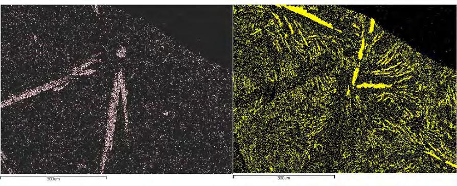
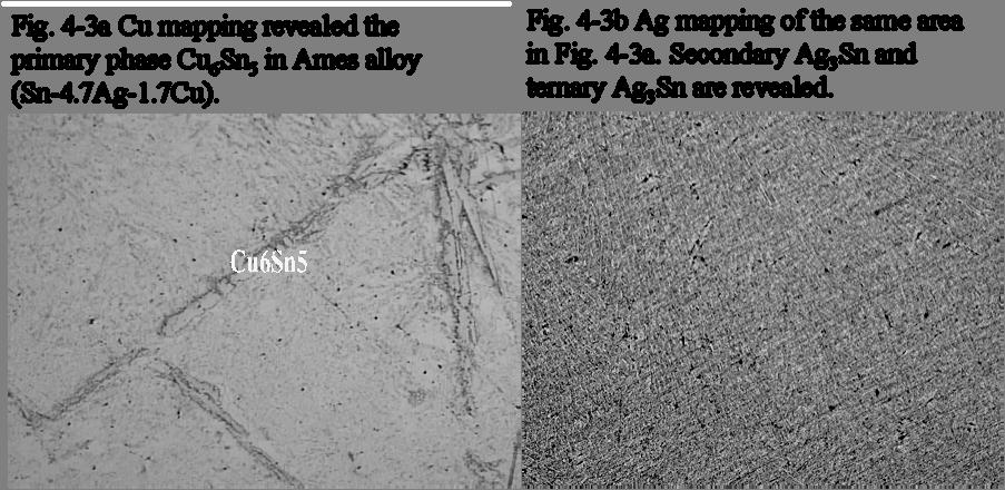
51 51 Table 4-4 Compositions of Sn-Ag-Cu alloys investigated in this work
52 Comparison of HUT alloy and Ames alloy In order to see the effects of composition on mechanical properties, Sn-Ag-Cu alloys with the eutectic composition of Sn-3.4Ag-0.8Cu determined by Helsinki University of Technology (HUT) (referred as HUT alloy hereafter) and Ames Lab (Sn-4.7Ag-1.7Cu [140,141], referred as Ames alloy hereafter) were compared in terms of shear strength, creep behavior, and microstructure. Rigid low carbon steel was used to make pins for the grooved lap joints. Solder joints were cooled in glycerol at a cooling rate that was slow enough to let IMC crystals form and grow. Fig. 4-5 shows the joint appearance of the two alloys. HUT alloy has fine eutectic microstructure but Ames alloy has the plate like IMCs inside the joint. The plate-like IMC crystals make the material and hence the solder joints harder and more brittle. Fig. 4-6 and Fig. 4-7 present the shear strength and creep behavior of the two alloys. Each alloy had two samples. HUT alloy had higher shear strength. It should be noted that the shear strength is variable with the change of shear speed and the cooling rate after reflow. Thermal aging also has influence on the shear strength [23]. HUT alloy also had better creep behavior than the Ames alloy. This difference is not surprising because the coarsened primary and secondary IMCs in the Ames alloy degrades the creep property of the joints. The creep behavior is not greatly dependent on cooling rate or external conditions. 4.3 Design of Sn-Ag-Cu solder composition Although the eutectic SnAgCu solder possesses overall good mechanical properties, it is not necessarily the best for all applications. To design a solder alloy for a specific application one needs to consider several factors such as surface finish materials, substrate and/or PWB thicknesses, package structures, die size and thickness which could change the joint stress situations.
53 53 Fig. 4-5 External appearance (upper pictures) and cross section of Sn-Ag-Cu solder joints bottom pictures). Left column: Ames solder. Plate-like IMC are clearly seen. Right column: HUT solder joint. No plate-like IMC was found. Both joints were cooled in Glycerol. Elastic modulus of the SnAgCu solder increases with Ag content. The elastic modulus of Sn4.0Ag0.5Cu solder is 53.3 GPa, but it is 47 GPa for Sn1.0Ag0.5Cu. In comparison, it is 40.2 GPa for SnPb eutectic solder [54]. This indicates that the lower the Ag content, the softer the SnAgCu solder balls. During drop tests of BGA package assemblies (Fig. 2-5b), a PWB assembly experiences high frequency bending [13] and the solder joints are under tensile stress. Under this condition, if the bulk solder is stiff, the stress is concentrated in the corner area between solder ball and UBM pad, and leads to interfacial fracture. If the solder can deform to such an extent that the stress is at least partially released, the joints will fail at a later time at the interface or within the bulk solder by ductile fracture. However, during thermal cycling, the BGA joints are mainly under shearing stress due to the smaller CTE mismatch between PWB and BGA substrate. The failure mode is usually fatigue of bulk solder. In this situation, high Ag solder has a higher thermal cycling (T/C) performance. This is because more Ag 3 Sn particles in solder slow down the propagation of the micro cracks and the solder is more resistant to thermal fatigue. Therefore, for BGA assembly interconnections whose main requirement is thermal
54 54 cycling performance, a high Ag content solder is preferred, but it should be lower than 3.5 wt. % to avoid formation of large plates of Ag 3 Sn. The low Ag solder is better for drop performance of BGA package assemblies [51]. Fig. 4-6 Shear stress at room temperature. Joint cooled in Glycerol. Fig. 4-7 Creep behavior of joints tested under 350N at room temperature. Joints cooled in Glycerol


55 55 For WLCSP, the situation is somewhat different. The solder joints are located between two materials that have a larger CTE mismatch (see Fig. 2-5a). Since the Si die is rigid, when the temperature increases, the PWB bends much more than in a BGA-PWB assembly and causes higher stress on solder joints. After multiple reflows, the PWB warpage will increase. As a result, the solder balls of WLCSP are under much higher tensile stress than BGA solder balls during reflow and thermal cycling, as schematically illustrated in Fig Therefore, the thermal cycling performance of WLCSP was mainly determined by the tensile stress in the solder joints rather than the shear stress as in the BGA packages. Consequently, the effect of Ag content of solder joints on thermal cycling performance of WLCSP was similar to that on drop performance of BGA packages. A low Ag solder gave better thermal cycling performance. Fig. 4-8 Schematic illustration of stress situation in solder joints at the high temperature dwell of thermal cycling. PWB thickness in WLCSP also plays an important role. At a given temperature, the stress caused by PWB warpage strongly depends on its thickness. It is more difficult to bend a thick PWB to the same level of warpage than a thinner PWB. As a result, the PWB warpage resulted in high tensile stress in solder joints. In order to improve the package reliability, a soft solder is required to release the tensile stress. Similar to Ag content, high Cu content in solder increases Cu 6 Sn 5 IMC and thus increases the elastic module of the solder balls. If Ni/Au plating is used as discussed in section 3.2.1, a small variation of Cu content in the range of wt.% can alter
56 56 interfacial IMC formation, morphology, thickness and eventually the joint reliability [9-11,145]. 5. Evaluation methods for package interconnection reliability Evaluation methods for package interconnection reliability usually have their standard specifications published by JEDEC ( and IPC ( Companies like Nokia and Motorola have their own test specifications with special objectives. The test plans are typically constructed with many variables so that the reliabilities of different combinations of the variables can be compared. Mechanical loading stress and temperature are most common variables used for reliability tests. The raw data obtained from the tests can be analyzed by statistical methods such as Weibull analysis. In this study, JEDEC standard drop test was carried out and Weibull analysis was employed to analyze the raw data of Pb-free assembly performance. Isothermal aging at different temperatures was applied to solder joints to examine the effect of temperature on joint microstructure and reliability. To study potential risks of Sn-pest in Pb-free solders, low temperature storage was selected. In addition, a thermal cycling test was used to compare Pb-free and Sn-Pb solder joint ability of withstanding thermo-mechanical stresses induced by high and low temperature extremes. Given below are brief descriptions of the drop test, thermal aging, low temperature storage, thermal cycling and Weibull statistic analysis. 5.1 Drop test Drop test is a technique for measuring the durability of an assembly or device by subjecting it to a free fall from a predetermined height to a surface under prescribed conditions. Fig. 5-1 shows the schematic view of a drop tester with the sample mounted and the layout of the test board in this work. The test board is screw-mounted to the drop table at 4 corners with the packages facing downwards (Fig. 5-1b). Integrity of interconnection in the test board is monitored by in-situ measurement of electrical
![57 resistivity. The test specifications and criteria for failure, based on JEDEC standard JESD22-B111 [146], are listed below: Peak acceleration: 1500 g +/- 10 % Pulse duration: 1.](/docs-images/74/69954372/images/57-0.jpg "0 ms +/- 10 % Pulse shape: Half-sine waveform Failure criteria: Electric resistance >1500Ω Drop height: 1.4 m Failed daisy chain: Electric resistance >1500Ω for more than 3 drops in a roll of 5 Fig.")

57 57 resistivity. The test specifications and criteria for failure, based on JEDEC standard JESD22-B111 [146], are listed below: Peak acceleration: 1500 g +/- 10 % Pulse duration: 1.0 ms +/- 10 % Pulse shape: Half-sine waveform Failure criteria: Electric resistance >1500Ω Drop height: 1.4 m Failed daisy chain: Electric resistance >1500Ω for more than 3 drops in a roll of 5 Fig. 5-1 Schematic view of the drop tester with sample mounted and the layout of test board. a) Top view of test board and location of the components. b) Test board mounted on the drop tester. JESD22-B111 is a board level drop test standard. Many drop test studies are carried out with this specification. Marjamäki and Kivilahti [13] measured the longitudinal strain in the middle of the board layout on the opposite side of the board from the components
Effect of local grain distribution and Enhancement on edgebond applied wafer-level chip-scale package (WLCSP) thermal cycling performance
 thermal cycling performance") Effect of local grain distribution and Enhancement on edgebond applied wafer-level chip-scale package (WLCSP) thermal cycling performance 1 Tae-Kyu Lee, 2 Weidong Xie, 2 Steven Perng, 3 Edward Ibe, and
Effect of local grain distribution and Enhancement on edgebond applied wafer-level chip-scale package (WLCSP) thermal cycling performance 1 Tae-Kyu Lee, 2 Weidong Xie, 2 Steven Perng, 3 Edward Ibe, and
Effect of Process Variations on Solder Joint Reliability for Nickel-based Surface Finishes
 Effect of Process Variations on Solder Joint Reliability for Nickel-based Surface Finishes Hugh Roberts Atotech USA Inc., Rock Hill, SC, USA Sven Lamprecht, Gustavo Ramos and Christian Sebald Atotech Deutschland
Thermal cyclic test for Sn-4Ag-0.5Cu solders on high P Ni/Au and Ni/Pd/Au surface finishes
 Journal of Mechanical Engineering and Sciences (JMES) ISSN (Print): 2289-4659; e-issn: 2231-8380; Volume 9, pp. 1572-1579, December 2015 Universiti Malaysia Pahang, Malaysia DOI: http://dx.doi.org/10.15282/jmes.9.2015.4.0152
Future Electronic Devices Technology in Cosmic Space and Electroless Ni/Pd/Au Plating for High Density Semiconductor Package Substrate
 JAXA 25 rd Microelectronics Workshop Future Electronic Devices Technology in Cosmic Space and Electroless Ni/Pd/Au Plating for High Density Semiconductor Package Substrate November 2, 2012 Yoshinori Ejiri
Traditional Solder Materials
 Traditional Solder Materials Characteristics of tin-lead solders In Metal basics we showed how cooling curves are used to produce a composite thermal equilibrium (or phase ) diagram of the tin-lead system.
Ball shear strength and fracture mode of lead-free solder joints prepared using nickel nanoparticle doped flux
 Ball shear strength and fracture mode of lead-free solder joints prepared using nickel nanoparticle doped flux G. K. Sujan a, A. S. M. A. Haseeb a, *, Chong Hoe Jian b, Amalina Afifi a a Department of
The Morphology Evolution and Voiding of Solder Joints on QFN Central Pads with a Ni/Au Finish
 The Morphology Evolution and Voiding of Solder Joints on QFN Central Pads with a Ni/Au Finish Julie Silk 1, Jianbiao Pan 2, Mike Powers 1 1 Agilent Technologies, 1400 Fountaingrove Parkway, Santa Rosa,
A study aimed at characterizing the interfacial structure in a tin silver solder on nickel-coated copper plate during aging
 Sādhanā Vol. 33, Part 3, June 2008, pp. 251 259. Printed in India A study aimed at characterizing the interfacial structure in a tin silver solder on nickel-coated copper plate during aging D C LIN 1,
Chapter Outline Dislocations and Strengthening Mechanisms. Introduction
 Chapter Outline Dislocations and Strengthening Mechanisms What is happening in material during plastic deformation? Dislocations and Plastic Deformation Motion of dislocations in response to stress Slip
Composition/wt% Bal SA2 (SABI) Bal SA3 (SABI + Cu) Bal
 Bal SA3 (SABI + Cu) Bal") Improving Thermal Cycle and Mechanical Drop Impact Resistance of a Lead-free Tin-Silver-Bismuth-Indium Solder Alloy with Minor Doping of Copper Additive Takehiro Wada 1, Seiji Tsuchiya 1, Shantanu Joshi
Improving Thermal Cycle and Mechanical Drop Impact Resistance of a Lead-free Tin-Silver-Bismuth-Indium Solder Alloy with Minor Doping of Copper Additive Takehiro Wada 1, Seiji Tsuchiya 1, Shantanu Joshi
System Level Effects on Solder Joint Reliability
 System Level Effects on Solder Joint Reliability Maxim Serebreni 2004 2010 Outline Thermo-mechanical Fatigue of solder interconnects Shear and tensile effects on Solder Fatigue Effect of Glass Style on
Reliability of Pb-Free Solder Alloys in Demanding BGA and CSP Applications
 Reliability of Pb-Free Solder Alloys in Demanding BGA and CSP Applications Ranjit Pandher and Robert Healey Cookson Electronics 109 Corporate Blvd. South Plainfield, NJ 07080, USA Email: rpandher@cooksonelectronics.com
ENHANCING WLCSP RELIABILITY THROUGH BUILD-UP STRUCTURE IMPROVEMENTS AND NEW SOLDER ALLOYS
 ENHANCING WLCSP RELIABILITY THROUGH BUILD-UP STRUCTURE IMPROVEMENTS AND NEW SOLDER ALLOYS B. Rogers, M. Melgo, M. Almonte, S. Jayaraman, C. Scanlan, and T. Olson Deca Technologies, Inc 7855 S. River Parkway,
Welcome to SMTA Brazil Chapter Brook Sandy-Smith Dr. Ron Lasky Tim Jensen
 Welcome to SMTA Brazil Chapter 2013 Presented by Authors Ivan Castellanos Edward Briggs Brook Sandy-Smith Dr. Ron Lasky Tim Jensen Advantages / Concerns HP testing Mechanical properties New work Area ratio
MT 348 Outline No MECHANICAL PROPERTIES
 MT 348 Outline No. 1 2009 MECHANICAL PROPERTIES I. Introduction A. Stresses and Strains, Normal and Shear Loading B. Elastic Behavior II. Stresses and Metal Failure A. ʺPrincipal Stressʺ Concept B. Plastic
Study of the Interface Microstructure of Sn-Ag-Cu Lead-Free Solders and the Effect of Solder Volume on Intermetallic Layer Formation.
 Study of the Interface Microstructure of Sn-Ag-Cu Lead-Free Solders and the Effect of Solder Volume on Intermetallic Layer Formation. B. Salam +, N. N. Ekere, D. Rajkumar Electronics Manufacturing Engineering
ENHANCING MECHANICAL SHOCK PERFORMANCE USING EDGEBOND TECHNOLOGY
 ENHANCING MECHANICAL SHOCK PERFORMANCE USING EDGEBOND TECHNOLOGY Steven Perng, Tae-Kyu Lee, and Cherif Guirguis Cisco Systems, Inc. San Jose, CA, USA sperng@cisco.com Edward S. Ibe Zymet, Inc. East Hanover,
Reflow Profiling: Time a bove Liquidus
 Reflow Profiling: Time a bove Liquidus AIM/David Suraski Despite much research and discussion on the subject of reflow profiling, many questions and a good deal of confusion still exist. What is clear
Lead-Free Solder Bump Technologies for Flip-Chip Packaging Applications
 Lead-Free Solder Bump Technologies for Flip-Chip Packaging Applications Zaheed S. Karim 1 and Jim Martin 2 1 Advanced Interconnect Technology Ltd. 1901 Sunley Centre, 9 Wing Yin Street, Tsuen Wan, Hong
CREEP CREEP. Mechanical Metallurgy George E Dieter McGraw-Hill Book Company, London (1988)
") CREEP CREEP Mechanical Metallurgy George E Dieter McGraw-Hill Book Company, London (1988) Review If failure is considered as change in desired performance*- which could involve changes in properties and/or
CREEP CREEP Mechanical Metallurgy George E Dieter McGraw-Hill Book Company, London (1988) Review If failure is considered as change in desired performance*- which could involve changes in properties and/or
RELIABILITY OF DOPED LEAD-FREE SOLDER JOINTS UNDER ISOTHERMAL AGING AND THERMAL CYCLING
 As originally published in the SMTA Proceedings RELIABILITY OF DOPED LEAD-FREE SOLDER JOINTS UNDER ISOTHERMAL AGING AND THERMAL CYCLING Cong Zhao, Thomas Sanders, Chaobo Shen, Zhou Hai, John L. Evans,
IMC Layers Formed with Various Combinations of Solders and Surface Finishes and Their Effect on Solder Joint Reliability
 IMC Layers Formed with Various Combinations of Solders and Surface Finishes and Their Effect on Solder Joint Reliability Per-Erik Tegehall, Swerea IVF 4 th Electronic Materials and Assembly Processes for
Characterization of Coined Solder Bumps on PCB Pads
 Characterization of Coined Solder Bumps on PCB Pads Jae-Woong Nah, Kyung W. Paik, Won-Hoe Kim*, and Ki-Rok Hur** Department of Materials Sci. & Eng., Korea Advanced Institute of Science and Technology
BOARD LEVEL RELIABILITY COMPARISON OF LEAD FREE ALLOYS
 BOARD LEVEL RELIABILITY COMPARISON OF LEAD FREE ALLOYS Robert Darveaux, Corey Reichman, Sabira Enayet, Wen-Sung Hsu, and Win Thandar Swe Amkor Technology, Inc. Chandler, AZ, USA rdarv@amkor.com ABSTRACT
REWORKABLE EDGEBOND APPLIED WAFER-LEVEL CHIP-SCALE PACKAGE (WLCSP) THERMAL CYCLING PERFORMANCE ENHANCEMENT AT ELEVATED TEMPERATURE
 THERMAL CYCLING PERFORMANCE ENHANCEMENT AT ELEVATED TEMPERATURE") REWORKABLE EDGEBOND APPLIED WAFER-LEVEL CHIP-SCALE PACKAGE (WLCSP) THERMAL CYCLING PERFORMANCE ENHANCEMENT AT ELEVATED TEMPERATURE Tae-Kyu Lee, Ph.D. Portland State University Portland, OR, USA taeklee@pdx.edu
REWORKABLE EDGEBOND APPLIED WAFER-LEVEL CHIP-SCALE PACKAGE (WLCSP) THERMAL CYCLING PERFORMANCE ENHANCEMENT AT ELEVATED TEMPERATURE Tae-Kyu Lee, Ph.D. Portland State University Portland, OR, USA taeklee@pdx.edu
Solder Alloy Evolution and Development
 Solder Alloy Evolution and Development SMTA Boston November 4, 2018 Presented by Timothy O Neill, Technical Marketing Manager, AIM A Brief Review of Electronic Solders 1960 s to 2006 Tin/Lead (Sn/Pb) Solder
Adaption to scientific and technical progress under Directive 2002/95/EC
 . Adaption to scientific and technical progress under Directive 2002/95/EC Results previous evaluation Exemption No. 15 Lead in solders to complete a viable electrical connection between semiconductor
Phase Transformations in Metals Tuesday, December 24, 2013 Dr. Mohammad Suliman Abuhaiba, PE 1
 Ferrite - BCC Martensite - BCT Fe 3 C (cementite)- orthorhombic Austenite - FCC Chapter 10 Phase Transformations in Metals Tuesday, December 24, 2013 Dr. Mohammad Suliman Abuhaiba, PE 1 Why do we study
Adaption to scientific and technical progress under Directive 2002/95/EC
 . Adaption to scientific and technical progress under Directive 2002/95/EC Results previous evaluation Exemption No. 7 a a) Lead in high melting temperature type solders (i.e. lead-based alloys containing
Future Electronic Devices Technology in Cosmic Space and Lead-free Solder Joint Reliability
 The 22nd Microelectronics Work Future Electronic Devices Technology in Cosmic Space and Lead-free Solder Joint Reliability Key Points (1) High Speed Solder Ball Shear Test (2) Relationship between Surface
EFFECT OF THERMAL AGING ON THE IMC LAYER BETWEEN SnAgSb SOLDER AND Cu SUBSTRATE. Universiti Kebangsaan Malaysia, 43600, Bangi, Selangor, Malaysia
 EFFECT OF THERMAL AGING ON THE IMC LAYER BETWEEN SnAgSb SOLDER AND Cu SUBSTRATE W. Shualdi 1, I. Ahmad 1, G. Omar 2 and A. Isnin 3 1 Department of Electrical, Electronic and System, Faculty of Engineering,
WF6317. A superactive low-volatile/high heat-resistant water-soluble flux for ball soldering
 WF637 A superactive low-volatile/high heat-resistant water-soluble flux for ball soldering Low viscosity and high tacking power stabilize ball holding force and ensures excellent solder wettability Easy
ME 254 MATERIALS ENGINEERING 1 st Semester 1431/ rd Mid-Term Exam (1 hr)
") 1 st Semester 1431/1432 3 rd Mid-Term Exam (1 hr) Question 1 a) Answer the following: 1. Do all metals have the same slip system? Why or why not? 2. For each of edge, screw and mixed dislocations, cite
1 st Semester 1431/1432 3 rd Mid-Term Exam (1 hr) Question 1 a) Answer the following: 1. Do all metals have the same slip system? Why or why not? 2. For each of edge, screw and mixed dislocations, cite
Sample Preparation for Mitigating Tin Whiskers in alternative Lead-Free Alloys
 As originally published in the IPC APEX EXPO Conference Proceedings. Sample Preparation for Mitigating Tin Whiskers in alternative Lead-Free Alloys Mehran Maalekian Karl Seelig, V.P. Technology Timothy
Evaluation of Pb-free BGA Solder Joint Reliability on Ni-based Surface Finishes using Alternative Shear and Pull Metrologies
 Evaluation of Pb-free BGA Solder Joint Reliability on Ni-based Surface Finishes using Alternative Shear and Pull Metrologies Kuldip Johal and Hugh Roberts Atotech USA Inc., Rock Hill, SC Sven Lamprecht,
EFFECT OF Ag COMPOSITION, DWELL TIME AND COOLING RATE ON THE RELIABILITY OF Sn-Ag-Cu SOLDER JOINTS. Mulugeta Abtew
 EFFECT OF Ag COMPOSITION, DWELL TIME AND COOLING RATE ON THE RELIABILITY OF Sn-Ag-Cu SOLDER JOINTS Mulugeta Abtew Typical PCB Assembly Process PCB Loading Solder Paste Application Solder Paste Inspection
Australian Journal of Basic and Applied Sciences. Pb-Free Solder Ball Robustness Comparison under AC and TC Reliability Test
 AENSI Journals Australian Journal of Basic and Applied Sciences ISSN:1991-8178 Journal home page: www.ajbasweb.com Pb-Free Solder Ball Robustness Comparison under AC and TC Reliability Test 1,2 Tan Cai
Reliability of RoHS-Compliant 2D and 3D 1С Interconnects
 Reliability of RoHS-Compliant 2D and 3D 1С Interconnects John H. Lau, Ph.D. New York Chicago San Francisco Lisbon London Madrid Mexico City Milan New Delhi San Juan Seoul Singapore Sydney Toronto Foreword
Thermo-Mechanical FEM Analysis of Lead Free and Lead Containing Solder for Flip Chip Applications
 Thermo-Mechanical FEM Analysis of Lead Free and Lead Containing Solder for Flip Chip Applications M. Gonzalez 1, B. Vandevelde 1, Jan Vanfleteren 2 and D. Manessis 3 1 IMEC, Kapeldreef 75, 3001, Leuven,
Reliability of Lead-Free Solder Connections for Area-Array Packages
 Presented at IPC SMEMA Council APEX SM 2001 For additional information, please email marketing@amkor.com Reliability of Lead-Free Solder Connections for Area-Array Packages Ahmer Syed Amkor Technology,
TEMPERATURE CYCLING AND FATIGUE IN ELECTRONICS
 TEMPERATURE CYCLING AND FATIGUE IN ELECTRONICS Gilad Sharon, Ph.D. DfR Solutions Beltsville, MD, USA gsharon@dfrsolutions.com Greg Caswell DfR Solutions Liberty Hill, TX, USA gcaswell@dfrsolutions.com
Mean-time-to-failure study of flip chip solder joints on CuÕNi V ÕAl thin-film under-bump-metallization
 JOURNAL OF APPLIED PHYSICS VOLUME 94, NUMBER 9 1 NOVEMBER 2003 Mean-time-to-failure study of flip chip solder joints on CuÕNi V ÕAl thin-film under-bump-metallization W. J. Choi, a) E. C. C. Yeh, b) and
The Development of the High Strength Aluminum Alloy Wire
 Special Issue OneF Automotive Technology The Development of the High Strength Aluminum Alloy Wire Sho Yoshida *, Shigeki Sekiya *, Kengo Mitose * The development of the high strength aluminum alloy wire,
Introduction to Engineering Materials ENGR2000 Chapter 7: Dislocations and Strengthening Mechanisms. Dr. Coates
 Introduction to Engineering Materials ENGR2000 Chapter 7: Dislocations and Strengthening Mechanisms Dr. Coates An edge dislocation moves in response to an applied shear stress dislocation motion 7.1 Introduction
SCV Chapter, CPMT Society, IEEE September 14, Voids at Cu / Solder Interface and Their Effects on Solder Joint Reliability
 Voids at / Solder Interface and Their Effects on Solder Joint Reliability Zequn Mei, Mudasir Ahmad, Mason Hu, Gnyaneshwar Ramakrishna Manufacturing Technology Group Cisco Systems, Inc. Acknowledgement:
Strengthening Mechanisms
 ME 254: Materials Engineering Chapter 7: Dislocations and Strengthening Mechanisms 1 st Semester 1435-1436 (Fall 2014) Dr. Hamad F. Alharbi, harbihf@ksu.edu.sa November 18, 2014 Outline DISLOCATIONS AND
HOW THE MOLD COMPOUND THERMAL EXPANSION OVERRULES THE SOLDER COMPOSITION CHOICE IN BOARD LEVEL RELIABILITY PERFORMANCE
 HOW THE MOLD COMPOUND THERMAL EXPANSION OVERRULES THE SOLDER COMPOSITION CHOICE IN BOARD LEVEL RELIABILITY PERFORMANCE AUTHORS: B. VANDEVELDE, L. DEGRENDELE, M. CAUWE, B. ALLAERT, R. LAUWAERT, G. WILLEMS
Fracture. Brittle vs. Ductile Fracture Ductile materials more plastic deformation and energy absorption (toughness) before fracture.
 before fracture.") 1- Fracture Fracture: Separation of a body into pieces due to stress, at temperatures below the melting point. Steps in fracture: 1-Crack formation 2-Crack propagation There are two modes of fracture depending
1- Fracture Fracture: Separation of a body into pieces due to stress, at temperatures below the melting point. Steps in fracture: 1-Crack formation 2-Crack propagation There are two modes of fracture depending
Shear Strength in Solder Bump Joints for High Reliability Photodiode Packages
 Materials Transactions, Vol. 44, No. 10 (2003) pp. 2163 to 2168 #2003 The Japan Institute of Metals Shear Strength in Solder Bump Joints for High Reliability Photodiode Packages Chong-Hee Yu 1, Kyung-Seob
Chapter 8 Strain Hardening and Annealing
 Chapter 8 Strain Hardening and Annealing This is a further application of our knowledge of plastic deformation and is an introduction to heat treatment. Part of this lecture is covered by Chapter 4 of
1) Fracture, ductile and brittle fracture 2) Fracture mechanics
 Fracture, ductile and brittle fracture 2) Fracture mechanics") Module-08 Failure 1) Fracture, ductile and brittle fracture 2) Fracture mechanics Contents 3) Impact fracture, ductile-to-brittle transition 4) Fatigue, crack initiation and propagation, crack propagation
Module-08 Failure 1) Fracture, ductile and brittle fracture 2) Fracture mechanics Contents 3) Impact fracture, ductile-to-brittle transition 4) Fatigue, crack initiation and propagation, crack propagation
Chapter 7 Dislocations and Strengthening Mechanisms. Dr. Feras Fraige
 Chapter 7 Dislocations and Strengthening Mechanisms Dr. Feras Fraige Chapter Outline Dislocations and Strengthening Mechanisms What is happening in material during plastic deformation? Dislocations and
THE EFFECTS OF Bi AND AGING ON THE MICROSTRUCTURE AND MECHANICAL PROPERTIES OF Sn-RICH ALLOYS
 THE EFFECTS OF Bi AND AGING ON THE MICROSTRUCTURE AND MECHANICAL PROPERTIES OF Sn-RICH ALLOYS André Delhaise and Doug Perovic University of Toronto Toronto, ON, Canada andre.delhaise@mail.utoronto.ca Polina
Effects of Lead on Tin Whisker Elimination
 Effects of Lead on Tin Whisker Elimination Wan Zhang and Felix Schwager Rohm and Haas Electronic Materials Lucerne, Switzerland inemi Tin Whisker Workshop at ECTC 0 May 30, 2006, in San Diego, CA Efforts
Composition/wt% Bal SA2 (SABI) Bal SA3 (SABI + Cu) Bal
 Bal SA3 (SABI + Cu) Bal") Improving Thermal Cycle and Mechanical Drop Impact Resistance of a Lead-free Tin-Silver-Bismuth-Indium Solder Alloy with Minor Doping of Copper Additive Takehiro Wada 1, Seiji Tsuchiya 1, Shantanu Joshi
Improving Thermal Cycle and Mechanical Drop Impact Resistance of a Lead-free Tin-Silver-Bismuth-Indium Solder Alloy with Minor Doping of Copper Additive Takehiro Wada 1, Seiji Tsuchiya 1, Shantanu Joshi
Growth Kinetics of Reaction Layers in Flip Chip Joints with Cu-cored Lead-free Solder Balls
 Materials Transactions, Vol. 5, No. 3 () pp. 75 to 75 Special Issue on Lead-Free Soldering in Electronics # The Japan Institute of Metals Growth Kinetics of Reaction Layers in Flip Chip Joints with Cu-cored
Design for Plastic Ball Grid Array Solder Joint Reliability. S.-W. R. Lee, J. H. Lau*
 Page 1 of 9 Design for Plastic Ball Grid Array Solder Joint Reliability The Authors S.-W. R. Lee, J. H. Lau* S.-W. R. Lee, Department of Mechanical Engineering, The Hong Kong University of Science and
Tutorial 2 : Crystalline Solid, Solidification, Crystal Defect and Diffusion
 Tutorial 1 : Introduction and Atomic Bonding 1. Explain the difference between ionic and metallic bonding between atoms in engineering materials. 2. Show that the atomic packing factor for Face Centred
3D-WLCSP Package Technology: Processing and Reliability Characterization
 3D-WLCSP Package Technology: Processing and Reliability Characterization, Paul N. Houston, Brian Lewis, Fei Xie, Ph.D., Zhaozhi Li, Ph.D.* ENGENT Inc. * Auburn University ENGENT, Inc. 2012 1 Outline Packaging
Gold to gold thermosonic bonding Characterization of bonding parameters
 Gold to gold thermosonic bonding Characterization of bonding parameters Thi Thuy Luu *1, Hoang-Vu Nguyen 1, Andreas Larsson 2, Nils Hoivik 1 and Knut E.Aasmundtveit 1 1: Institute of Micro and Nanosystems
Micro-Impact Test on Lead-Free BGA Balls on Au/Electrolytic Ni/Cu Bond Pad
 Micro- Test on Lead-Free BGA Balls on Au/Electrolytic Ni/Cu Bond Pad Shengquan Ou*, Yuhuan Xu and K. N. Tu Department of Materials Science and Engineering, UCLA, Los Angeles, CA, 90095-1595 M. O. Alam,
The Effects of Aging on the Reliability of Lead Free Fine-Pitch Electronics Packaging. Jiawei Zhang
 The Effects of Aging on the Reliability of Lead Free Fine-Pitch Electronics Packaging by Jiawei Zhang A dissertation submitted to the Graduate Faculty of Auburn University in partial fulfillment of the
Simulations and Characterizations for Stress Reduction Designs in Wafer Level Chip Scale Packages
 Simulations and Characterizations for Stress Reduction Designs in Wafer Level Chip Scale Packages by Ming-Che Hsieh STATS ChipPAC Taiwan Co. Ltd. Copyright 2013. Reprinted from 2013 International Microsystems,
Fundamentals of Plastic Deformation of Metals
 We have finished chapters 1 5 of Callister s book. Now we will discuss chapter 10 of Callister s book Fundamentals of Plastic Deformation of Metals Chapter 10 of Callister s book 1 Elastic Deformation
T/C stress resistant high reliability solder alloy SB6NX / SB6N. Patented by Panasonic
 T/C stress resistant high reliability solder alloy X / Patented by Panasonic Sn 3.5Ag 0.5Bi 6.0In 0.8Cu Sn 3.5Ag 0.5Bi 6.0In X & solder alloy X alloy is Panasonic patented Conventional (Sn3.5Ag0.5Bi6In)
Learning Objectives. Chapter Outline. Solidification of Metals. Solidification of Metals
 Learning Objectives Study the principles of solidification as they apply to pure metals. Examine the mechanisms by which solidification occurs. - Chapter Outline Importance of Solidification Nucleation
Interfacial Reactions between the Sn-9Zn Solder and Au/Ni/SUS304 Multi-layer Substrate
 , July 6-8, 2011, London, U.K. Interfacial Reactions between the Sn-9Zn Solder and Au/Ni/SUS304 Multi-layer Substrate *Yee-Wen Yen 1, Chien-Chung Jao 2, Kuo-Sing Chao 1, Shu-Mei Fu Abstract Sn-9Zn lead-free
Reaction of Sn-Bearing Solders with Nickel-based Under Bump Metallisations
 STR/03/069/ST Reaction of Sn-Bearing Solders with Nickel-based Under Bump Metallisations G. Qi, M. He and Z. Chen Abstract This work relates to wafer bumping technologies for flip chip packaging applications
Thermal Fatigue Evaluation of Pb-Free Solder Joints: Results, Lessons Learned, and Future Trends
 JOM, Vol. 67, No. 10, 2015 DOI: 10.1007/s11837-015-1595-1 2015 The Minerals, Metals & Materials Society Thermal Fatigue Evaluation of Pb-Free Solder Joints: Results, Lessons Learned, and Future Trends
Effects of Bi Content on Mechanical Properties and Bump Interconnection Reliability of Sn-Ag Solder Alloys
 Effects of Bi Content on Mechanical Properties and Bump Interconnection Reliability of Sn-Ag Solder Kazuki Tateyama, Hiroshi Ubukata*, Yoji Yamaoka*, Kuniaki Takahashi*, Hiroshi Yamada** and Masayuki Saito
THE EFFECTS OF INTERNAL STRESSRS IN BGA Ni LAYER ON THE STRENGTH OF Sn/Ag/Cu SOLDER JOINT
 THE EFFECTS OF INTERNAL STRESSRS IN BGA Ni LAYER ON THE STRENGTH OF Sn/Ag/Cu SOLDER JOINT C.H. Chien 1, * C.J. Tseng 1,2 T.P. Chen 1,3 1 Department of Mechanical and Electro-Mechanical Engineering, National
Development and characterization of novel metallic joint in power electronic device
 Development and characterization of novel metallic joint in power electronic device Guillaume LACOMBE 1-a, Jean-Marc HEINTZ 1-b, Akira KAWASAKI 2-c, Jean-François SILVAIN 1-d 1 CNRS, Université de Bordeaux,
Chapter Outline: Failure
 Chapter Outline: Failure How do Materials Break? Ductile vs. brittle fracture Principles of fracture mechanics Stress concentration Impact fracture testing Fatigue (cyclic stresses) Cyclic stresses, the
Strengthening Mechanisms. Today s Topics
 MME 131: Lecture 17 Strengthening Mechanisms Prof. A.K.M.B. Rashid Department of MME BUET, Dhaka Today s Topics Strengthening strategies: Grain strengthening Solid solution strengthening Work hardening
IMPACT OF LEAD-FREE COMPONENTS AND TECHNOLOGY SCALING FOR HIGH RELIABILITY APPLICATIONS
 IMPACT OF LEAD-FREE COMPONENTS AND TECHNOLOGY SCALING FOR HIGH RELIABILITY APPLICATIONS Chris Bailey, Ph.D. University of Greenwich London, United Kingdom c.bailey@gre.ac.uk ABSTRACT Semiconductor technology
Recrystallization of Sn Grains due to Thermal Strain in Sn-1.2Ag-0.5Cu-0.05Ni Solder
 Materials Transactions, Vol. 45, No. 4 (2004) pp. 1383 to 1390 #2004 The Japan Institute of Metals EXPRESS REGULAR ARTICLE Recrystallization of Sn Grains due to Thermal Strain in Sn-1.2Ag-0.5Cu-0.05Ni
Materials Science and Engineering: An Introduction
 Materials Science and Engineering: An Introduction Callister, William D. ISBN-13: 9780470419977 Table of Contents List of Symbols. 1 Introduction. 1.1 Historical Perspective. 1.2 Materials Science and
CHAPTER 3 SELECTION AND PROCESSING OF THE SPECIMEN MATERIAL
 54 CHAPTER 3 SELECTION AND PROCESSING OF THE SPECIMEN MATERIAL 3.1 HIGH STRENGTH ALUMINIUM ALLOY In the proposed work, 7075 Al alloy (high strength) has been identified, as a material for the studies on
MECHANICAL PROPERTIES OF Sn3.5Ag AND Sn3.8Ag0.7Cu SOLDER BALLS FOR BGA PACKAGE
 221 MECHANICAL PROPERTIES OF AND Sn3.8Ag0.7Cu SOLDER BALLS FOR BGA PACKAGE A. Jalar 1, B.Y. Majlis 2, I.Ahmad 2 and E.P. Leng 3 1 School of Applied Physics, University Kebangsaan Malaysia, Selangor, Malaysia
Silver Diffusion Bonding and Layer Transfer of Lithium Niobate to Silicon
 Chapter 5 Silver Diffusion Bonding and Layer Transfer of Lithium Niobate to Silicon 5.1 Introduction In this chapter, we discuss a method of metallic bonding between two deposited silver layers. A diffusion
STRENGTHENING MECHANISM IN METALS
 Background Knowledge Yield Strength STRENGTHENING MECHANISM IN METALS Metals yield when dislocations start to move (slip). Yield means permanently change shape. Slip Systems Slip plane: the plane on which
Lead Free Soldering Technology
 Lead Free Soldering Technology Chung-Ang University Young-Eui Shin Trend of Package Small, Light, High performance High speed, Large capacity High integrity, High density Comparison of package size 45mm
Grain Refinement for Improved Lead-Free Solder Joint Reliability
 Grain Refinement for Improved Lead-Free Solder Joint Reliability K. Sweatman 1, S. D. McDonald 2, M. Whitewick 2, T. Nishimura 1, and K. Nogita 2 1. Nihon Superior Co., Ltd, Osaka, Japan 2. University
Solder joint reliability of plastic ball grid array with solder bumped flip chip
 ball grid array with solder bumped Shi-Wei Ricky Lee Department of Mechanical Engineering, The Hong Kong University of Science and, Kowloon, Hong Kong John H. Lau Express Packaging Systems, Inc., Palo
Title. CitationElectronics Goes Green (EGG 2004) September 6- Issue Date Doc URL
 September 6- Issue Date Doc URL") Title Development of Micro-structured Sn-2Ag-0.1Al Solder Author(s)Tanaka, Junichi; Takashima, Toshiyuki; Yoshimi, Kenj CitationElectronics Goes Green 2004+ (EGG 2004) September 6- Issue Date 2004-09 Doc
Title Development of Micro-structured Sn-2Ag-0.1Al Solder Author(s)Tanaka, Junichi; Takashima, Toshiyuki; Yoshimi, Kenj CitationElectronics Goes Green 2004+ (EGG 2004) September 6- Issue Date 2004-09 Doc
Lead-Contamination in Lead-Free Electronics Assembly Karl Seelig and David Suraski AIM
 Lead-Contamination in Lead-Free Electronics Assembly Karl Seelig and David Suraski AIM The question of what happens to a lead-free solder joint if it becomes contaminated with lead is important because
Lecture 12: High Temperature Alloys
 Part IB Materials Science & Metallurgy H. K. D. H. Bhadeshia Course A, Metals and Alloys Lecture 12: High Temperature Alloys Metallic materials capable of operating at ever increasing temperatures are
THE EFFECTS OF PLATING MATERIALS, BOND PAD SIZE AND BOND PAD GEOMETRY ON SOLDER BALL SHEAR STRENGTH
 THE EFFECTS OF PLATING MATERIALS, BOND PAD SIZE AND BOND PAD GEOMETRY ON SOLDER BALL SHEAR STRENGTH Keith Rogers and Craig Hillman CALCE Electronic Products and Systems Center University of Maryland College
New Assembly Technologies for T jmax =175 C Continuous Operation Guaranty of IGBT Module
 New Assembly Technologies for T jmax =175 C Continuous Operation Guaranty of IGBT Module MOMOSE Fumihiko SAITO Takashi NISHIMURA Yoshitaka ABSTRACT In order to meet the needs for miniaturization and cost
Schematic representation of the development of microstructure. during the equilibrium solidification of a 35 wt% Ni-65 wt% Cu alloy
 Schematic representation of the development of microstructure during the equilibrium solidification of a 35 wt% Ni-65 wt% Cu alloy At 1300 ºC (point a) the alloy is in the liquid condition This continues
TIN-BASED LEAD-FREE SOLDER BUMPS FOR FLIP-CHIP APPLICATION. S. Yaakup, H. S. Zakaria, M. A. Hashim and A. Isnin
 TIN-BASED LEAD-FREE SOLDER BUMPS FOR FLIP-CHIP APPLICATION S. Yaakup, H. S. Zakaria, M. A. Hashim and A. Isnin Advanced Materials Research Centre (AMREC), SIRIM Berhad, Lot 34, Jalan Hi-Tech 2/3, Kulim
Discrete Capacitor & Resistor Issues. Anthony Primavera Boston Scientific CRM 11/13/06
 Discrete Capacitor & Resistor Issues Anthony Primavera Boston Scientific CRM 11/13/06 Goal: Drive the Industry towards common test methods and best practices in manufacturing to reduce and or eliminate
Introduction to Materials Science
 EPMA Powder Metallurgy Summer School 27 June 1 July 2016 Valencia, Spain Introduction to Materials Science Prof. Alberto Molinari University of Trento, Italy Some of the figures used in this presentation
Combined Thermodynamic-Kinetic Analysis of the Interfacial Reactions between Ni Metallization and Various Lead-Free Solders
 Materials 2009, 2, 1796-1834; doi:10.3390/ma2041796 Review OPEN ACCESS materials ISSN 1996-1944 www.mdpi.com/journal/materials Combined Thermodynamic-Kinetic Analysis of the Interfacial Reactions between
This document is downloaded from DR-NTU, Nanyang Technological University Library, Singapore.
 This document is downloaded from DR-NTU, Nanyang Technological University Library, Singapore. Title Author(s) Citation Effect of post-reflow cooling rate on intermetallic compound formation between Sn
Analysis of plating grain size effect on whisker
 Journal of Mechanical Science and Technology 23 (2009) 2885~2890 Journal of Mechanical Science and Technology www.springerlink.com/content/1738-494x DOI 10.1007/s12206-009-0720-x Analysis of plating grain
Diffusion controlled growth of phases in metal tin systems related to microelectronics packaging. Guides: Prof. Aloke Paul and Prof.
 Diffusion controlled growth of phases in metal tin systems related to microelectronics packaging Ph.D. thesis Varun A Baheti, Department of Materials Engineering, Indian Institute of Science Guides: Prof.
Improving mechanical and electrical properties of Cu/SAC305/Cu solder joints under electromigration by using Ni nanoparticles doped flux
 https://doi.org/10.1007/s10854-017-8252-0 Improving mechanical and electrical properties of Cu/SAC305/Cu solder joints under electromigration by using Ni nanoparticles doped flux M. Nasir Bashir 1 A. S.
Comparative study of the dissolution kinetics of electrolytic Ni and electroless Ni P by the molten Sn3.5Ag0.5Cu solder alloy
 Microelectronics Reliability 43 (2003) 2031 2037 www.elsevier.com/locate/microrel Comparative study of the dissolution kinetics of electrolytic Ni and electroless Ni P by the molten Sn3.5Ag0.5Cu solder
Intermetallic Reactions in a Sn-20In-2.8Ag Solder Ball-Grid-Array Package with Au/Ni/Cu Pads
 Journal of ELECTRONIC MATERIALS, Vol. 34, No. 11, 2005 Regular Issue Paper Intermetallic Reactions in a Sn-20In-2.8Ag Solder Ball-Grid-Array Package with Au/Ni/Cu Pads HUI-MIN WU, 1,2 FENG-CHIH WU, 1 and