3D-EBSD an CrossBeam-Systemen
|
|
|
- Zoe McDowell
- 6 years ago
- Views:
Transcription


1 FIB- Workshop July D-EBSD an CrossBeam-Systemen Ulrike Zeile 1, Ali Gholinia 2 and Frank Bauer 3 Arbeitskreis FIB SSOM DGM/DGE ASEM Hotel Seeburg, Luzern, Switzerland 1. Carl Zeiss NTS 2. Oxford Instruments HKL A/S 3. OXFORD Instruments GmbH NanoAnalysis - Wiesbaden Fbauer07/2008


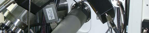
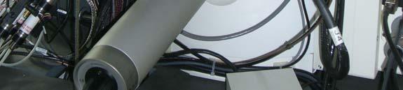


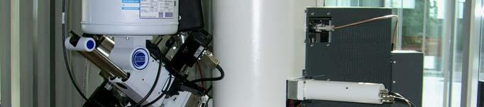
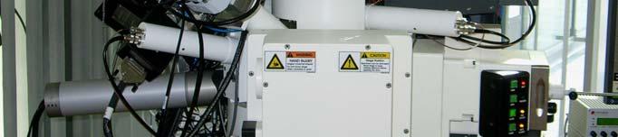
2 Nordlys Camera mounted on Crossbeam 1540EsB
3 NordlysF 400 advantages for 3-D EBSD Fastest EBSD detector available Drift mitigation Time for EBSD mapping portion of 3-D acquisition minimized 3-D EBSD can take tens of hours to days EBSD mapping is a major portion of that time Currently, only available with Zenith (thus Zeiss)


4 EBSD-Phosphor screen with forescatter-detectors ED-Detector: element analysis SEM pole piece Sample: tilted by 70 to improve interference contrast of scattered electrons Lower diode: Mainly orientation contrast, large angle scattered electrons Phosphor screen: converting electrons to photons Lowest diode: orientation contrast

5 Column and detector arrangement XB1540EsB 3-D EBSD requires very small working distances (~5 mm). SE FIB SEM The Nordlys design, especially the tapered nose, is a BIG advantage here EBSD -> ideale for 3D- EBSD


6 Forescatter Detector (FSD) BSE / FSE imaging with up to 6 detectors First information on phases and/or grain orientation BSE Z-contrast for phase differentiation (upper detectors). FSE orientation contrast for grain size and /or stress and strain imaging ( lower detectors)
7 Scheme of 3D-EBSD analysis Single image Acquisition Multiple image Acquisition Material Characterization and Conditioning Image Acquisition Multiple Image Acquisition Pattern Recognition & Analysis Software Image alignment FIB and image alignment Electron optic FIB equipment for Cross sections Image: BSE, FSE or SE Motorized sample stage Sample alignment Axes x,y,r,z,z Sample FIBing Cut- and polishing EBSD Camera: Pattern Acquisition Microscope or X-beam and Analysis Hardware Polished Samples, Stubs or other kind of material
 relative precision better than 1 absolute precision depends on correlation between sample CS and stage CS (>2 ) R Z")
8 Sample mounting in SEM Image coordination system Y Beam R X Y Randle, (1992) Microtexture Determination Institute of Materials Stage coordination system Orientation depends on the definition of cartesian coordination system (CS) relative precision better than 1 absolute precision depends on correlation between sample CS and stage CS (>2 ) R Z X
9 3D EBSD steps to go 1. Data acquisition and FIB control with the HKL Fast Acquisition Software 2. Data evaluation with HKL 3D-Viewer
10 Fast Acquisition : Data Collection easy control with Fast-Acquisition-Software Automized EBSD- Mapping and FIBing during complete time of acquisition and pattern interpretation High speed EBSD- Mapping by NordlysF400 camera on-line drift correction for automatic alignment of slides during acquisition and/or interpretation
11 Fast Acquisition : Data Collection No limitation in number of cuttings, of course dependend on thickness and sample size ( more than 12o slides tested ) Continued measuring, e.g. after interrupted acquisition No limitation in detection volume ( recommended volume less than 8000µm 3 ). High spatial resolution with EBSD, FIB and Alignment (20nm in x, y and z).
12 flexible EBSD stage Schematic view of the 55 pre-tilt sample holder

13 Chamber view

14 Chamber view during process ESV3.avi


15 Chamber view FIB position EBSD position EBSD

16 CrossBeam 3D-EBSD at Work
17 Software - Dialogue and Evaluation Carl-Zeiss (API) FIB SmartSEM OI-HKL (UIF) EBSD Acquisition Fast Acquisition OI-HKL (UIF) EBSD Post-Processing 3D Viewer Results
18 3D Viewer : Data processing and presentation Combining and cropping data of all individual slides Refinement and adjustment of layer positions ( Alignment ) Data presentation and export for individual grains
19 3D Viewer : Data processing and presentation 3D and free using 2D-planes in x,y and z with classical data presentations of EBSD-results and pole figures 3D noise reduction, based on voxels. 3D grain boundary reconstruction and visualization of grains. 3D orientation ellipsoidal sphere fitting on grains. 3D presentations and movies.


20 3D EBSD with Fast EBSD mapping Sample: Copper 51 layers 0.2µm resolution in X, Y and Z Number of voxels: 101x91x µm EBSD speed: 200^pic/s, 50 sec. per layer FIB speed: about 45 minutes per layer Total EBSD time: about 1 hour Total FIB time: about 38 hours Number of sessions/interupptions: 3


21 3D EBSD Data Presentation Note the blue grain in the next slide X Z Y Cross-sections in X, Y and Z planes Select and highlight a grain
 Y Y Coherent twin boundary")
22 Grain Boundary Analysis Z (2-11) (111) Y Y Coherent twin boundary Z
23 Grain Segmentation Data Region No. of Voxels Volume 1000x µm 3 Surface area µm 2 Mean Orientation, Euler angles, Mean Misorien -tation, Ellipsoid radii µm , 41.3, , 0.283, , 25.4, , 0.304, , 39.9, , 0.323, , 25.6, , 0.240, , 40.9, , 0.099, 0.054
24 Misorientation Data Regions Angle Axis X Axis Y Axis Z Direction Angle from <111> [1-1-1] [1-11] [-111] [1-11] 0.24 All misorientations are very close to 60 <111>
25 Dominant Axes Regions Dom. Axis X Dom. Axis Y Dom. Axis Z The table shows the direction of the boundary plane normal with respect to the sample coordinate system When converted to the crystal coordinate system, these are near to <111>. Therefore the boundary plane is near to {111}.

26 Fast Acquisition Program Pt - Draht

27 Data acquisition HKL Fast Acquisition Interface Pt-wire FIBcontrol

28 Data processing HKL 3D Viewer Pt-Wire IPF & Segments
29 Cropped Sections of Ti-Sample


30 Data processing HKL 3D Viewer individual grains Pt-pole figure of grain #1991
31 3D-View single grain
32 Conclusion 3D EBSD is a universal extensive tool for: 3D measurements for complete description of all grain / inclusion / particle form factors 3D characterization of grain boundaries 3D Analysis of micro texturs Vicinity effects of grains due to deformation or recrystallization Nucleation on recrystallization or phase transformation Epitaxy on CVD, PvD, LPE, etc. close to final end...
33 Possible limitations? Costs (SEM-FIB cross beam with 3D-EBSD Analysis) Practical limitations (time consuming analysis, analysis volumina, Isolators, material degradation from ions (FIB ), etc...) System stability over a long time period ( hours, days,...) Destructive method Huge data sets (3 dimensional data), for example 56MB for Pt-wire (42Schnitte)
EBSD Electron BackScatter Diffraction Principle and Applications
 EBSD Electron BackScatter Diffraction Principle and Applications Dr. Emmanuelle Boehm-Courjault EPFL STI IMX Laboratoire de Simulation des Matériaux LSMX emmanuelle.boehm@epfl.ch 1 Outline! Introduction!
Observation in the GB (Gentle Beam) Capabilities
 Capabilities") A field-emission cathode in the electron gun of a scanning electron microscope provides narrower probing beams at low as well as high electron energy, resulting in both improved spatial resolution and
A field-emission cathode in the electron gun of a scanning electron microscope provides narrower probing beams at low as well as high electron energy, resulting in both improved spatial resolution and
In-situ Heating Characterisation Using EBSD
 Webinar In-situ Heating Characterisation Using EBSD Speakers Dr. Ali Gholinia Dr. Neil Othen Dr. Jenny Goulden Topics Introduction to EBSD Why do in-situ experiments? EBSD equipment requirements for in-situ
Introduction to Electron Backscattered Diffraction. TEQIP Workshop HREXRD Feb 1 st to Feb 5 th 2016
 Introduction to Electron Backscattered Diffraction 1 TEQIP Workshop HREXRD Feb 1 st to Feb 5 th 2016 SE vs BSE 2 Ranges and interaction volumes 3 (1-2 m) http://www4.nau.edu/microanalysis/microprobe/interact-effects.html
Diffraction Contrast Tomography. Unlocking Crystallographic Information from Laboratory X-ray Microscopy. Technical Note
 Diffraction Contrast Tomography Unlocking Crystallographic Information from Laboratory X-ray Microscopy Technical Note Diffraction Contrast Tomography Unlocking Crystallographic Information from Laboratory
EBSD Basics EBSD. Marco Cantoni 021/ Centre Interdisciplinaire de Microscopie Electronique CIME. Phosphor Screen. Pole piece.
 EBSD Marco Cantoni 021/693.48.16 Centre Interdisciplinaire de Microscopie Electronique CIME EBSD Basics Quantitative, general microstructural characterization in the SEM Orientation measurements, phase
Texture Analysis in MSE
 Texture Analysis in MSE 집합조직제어연구실 서울대학교재료공학부 Texture (Preferred Orientation) Similarity of Texture E.T?! 한쪽을쳐다보고있는사람들여러방향을쳐다보는 Randomly Preferred Oriented What a Wonderful & Beautiful Life! Scientific
NEMI Sn Whisker Modeling Group Part 2:Future Work
 NEMI Sn Whisker Modeling Group Part 2:Future Work IPC/NEMI Meeting Maureen Williams, NIST Irina Boguslavsky, NEMI Consultant November 7, 2002 New Orleans, LA Capabilities of NEMI Modeling Group NEMI Fundamental
Mambo is the perfect tool for viewing EBSD data in pole and inverse pole figures.
 Mambo Pole figure and inverse pole figure software The physical properties of many samples are dependent on the common alignment of particular crystallographic directions: one of the easiest ways to view
Crystallographic Textures Measurement
 Crystallographic Textures Measurement D. V. Subramanya Sarma Department of Metallurgical and Materials Engineering Indian Institute of Technology Madras E-mail: vsarma@iitm.ac.in Macrotexture through pole
Applications of EBSD
 Applications of EBSD Dr. V. Subramanya Sarma Department of Metallurgical and Materials Engineering Indian Institute of Technology Madras E-mail: vsarma@iitm.ac.in Applications of EBSD Grain size distribution
Microstructural Controls on Trace Element Variability in Ore Minerals
 2 Microstructural Controls on Trace Element Variability in Ore Minerals Question: Does EBSD provide new insight into ore mineral microstructure and the chemical enrichment of elements in hydrothermal ore
ORIENTATION DETERMINATION BY EBSP IN AN ENVIRONMENTAL SCANNING ELECTRON MICROSCOPE
 Pergamon PII S1359-6462(99)00086-X Scripta Materialia, Vol. 41, No. 1, pp. 47 53, 1999 Elsevier Science Ltd Copyright 1999 Acta Metallurgica Inc. Printed in the USA. All rights reserved. 1359-6462/99/$
Focused Ion Beam CENTRE INTERDISCIPLINAIRE DE MICROSCOPIE ELECTRONIQUE. Marco Cantoni, EPFL-CIME CIME ASSEMBLEE GENERALE 2007
 Focused Ion Beam @ CENTRE INTERDISCIPLINAIRE DE MICROSCOPIE ELECTRONIQUE Present situation and vision Marco Cantoni, EPFL-CIME Dual Beam Nova 600 Nanolab from FEI Company FE-SEM & FIB: Ga LMIS 4 Gas Injector
Carnegie Mellon MRSEC
 Carnegie Mellon MRSEC Texture, Microstructure & Anisotropy, Fall 2009 A.D. Rollett, P. Kalu 1 ELECTRONS SEM-based TEM-based Koseel ECP EBSD SADP Kikuchi Different types of microtexture techniques for obtaining
Supplementary Materials for
 www.sciencemag.org/cgi/content/full/336/6084/1007/dc1 Supplementary Materials for Unidirectional Growth of Microbumps on (111)-Oriented and Nanotwinned Copper Hsiang-Yao Hsiao, Chien-Min Liu, Han-wen Lin,
THREE DIMENSIONAL MICROSTRUCTURAL CHARACTERIZATION OF CATHODE DEGRADATION IN SOFCS USING FOCUSED ION BEAM AND SEM
 THREE DIMENSIONAL MICROSTRUCTURAL CHARACTERIZATION OF CATHODE DEGRADATION IN SOFCS USING FOCUSED ION BEAM AND SEM Joshua Taillon, Christopher Pellegrinelli, Yilin Huang, Eric Wachsman, and Lourdes Salamanca-Riba
Multiphase analysis - combining EDS and EBSD
 Multiphase analysis - combining EDS and EBSD Outline Review: Conventional materials characterisation: Analysing polyphase materials using EDS Analysing polyphase materials using EBSD Combined EDS and EBSD
Liverpool, UK, L69 3GP
 Materials Science Forum Vols. 467-470 (2004) pp. 573-578 online at http://www.scientific.net 2004 Trans Tech Publications, Switzerland Using electron backscatter diffraction (EBSD) to measure misorientation
In-situ Observation of Microstructure Change in Steel by EBSD
 NIPPON STEEL & SUMITOMO METAL TECHNICAL REPORT No. 114 MARCH 2017 Technical Report UDC 621. 785. 36 In-situ Observation of Microstructure Change in Steel by EBSD Masayuki WAKITA* Seiichi SUZUKI Abstract
QUANTAX CrystAlign. Innovation with Integrity. Reinventing EBSD EBSD
 Reinventing EBSD QUANTAX CrystAlign Innovation with Integrity EBSD CrystAlign the User-friendly EBSD System Bruker s QUANTAX CrystAlign EBSD analysis system is the easy-to-use, multi-purpose tool for users
JSM-7800F Field Emission Scanning Electron Microscope
 JSM-7800F catalogue JSM-7800F Field Emission Scanning Electron Microscope We provide high performance The Ultimate Research Tool for Multi-Disciplinary Research Institutions Extreme resolution The super
LECTURE 7. Dr. Teresa D. Golden University of North Texas Department of Chemistry
 LECTURE 7 Dr. Teresa D. Golden University of North Texas Department of Chemistry Diffraction Methods Powder Method For powders, the crystal is reduced to a very fine powder or microscopic grains. The sample,
Electron Microscopy Studies of Niobium Thin Films on Copper
 Electron Microscopy Studies of Niobium Thin Films on Copper Roy Crooks 1, Greg Thompson 2, Robb Morris 2, Michelle Adams Hughes 3, Daudi Waryoba 3, and Peter Kalu 3 1 Black Laboratories, L.L.C., Newport
Grain Contrast Imaging in UHV SLEEM
 Materials Transactions, Vol. 51, No. 2 (2010) pp. 292 to 296 Special Issue on Development and Fabrication of Advanced Materials Assisted by Nanotechnology and Microanalysis #2010 The Japan Institute of
Fundamentals of X-ray diffraction and scattering
 Fundamentals of X-ray diffraction and scattering Don Savage dsavage@wisc.edu 1231 Engineering Research Building (608) 263-0831 X-ray diffraction and X-ray scattering Involves the elastic scattering of
AN INTRODUCTION TO OIM ANALYSIS
 AN INTRODUCTION TO OIM ANALYSIS Raising the standard for EBSD software The most powerful, flexible, and easy to use tool for the visualization and analysis of EBSD mapping data OIM Analysis - The Standard
> 3d imaging of ceramic CMC for numerical modelling - 91st annual meeting of the DKG - 8. March 2016
 www.dlr.de Chart 1 > 3d imaging of ceramic CMC for numerical modelling - 91st annual meeting of the DKG - 8. March 2016 3-dimensional microstructure characterization of porous ceramic matrix composites
Electron microscopy II
 Electron microscopy II Nanomaterials characterization I RNDr. Věra Vodičková, PhD. Interaction ction: electrons solid matter Signal types SE.secondary e - AE Auger s e - BSE back scattered e - X-ray photons,
Empirical constraints of shock features in monazite using shocked zircon inclusions
 GSA Data Repository 2016205 Empirical constraints of shock features in monazite using shocked zircon inclusions Erickson et al. DR 1 Analytical methods Identification of Shocked Monazites and Imaging External
ELECTRON BACKSCATTER DIFFRACTION (EBSD) THE METHOD AND ITS APPLICATIONS IN MATERIALS SCIENCE AND ENGINEERING
 THE METHOD AND ITS APPLICATIONS IN MATERIALS SCIENCE AND ENGINEERING") ELECTRON BACKSCATTER DIFFRACTION (EBSD) THE METHOD AND ITS APPLICATIONS IN MATERIALS SCIENCE AND ENGINEERING P. Cizek UNIVERSITY OF OXFORD, Department of Materials, Parks Road, Oxford OX1 3PH, GB Abstract
ELECTRON BACKSCATTER DIFFRACTION (EBSD) THE METHOD AND ITS APPLICATIONS IN MATERIALS SCIENCE AND ENGINEERING P. Cizek UNIVERSITY OF OXFORD, Department of Materials, Parks Road, Oxford OX1 3PH, GB Abstract
Changes in Microstructure of Al/AlN Interface during Thermal Cycling
 Materials Transactions, Vol. 49, No. 12 (2008) pp. 2808 to 2814 #2008 The Japan Institute of Metals Changes in Microstructure of / Interface during Thermal Cycling Yoshiyuki Nagatomo 1, Takeshi Kitahara
Appendix 1 TEXTURE A1.1 REPRESENTATION OF TEXTURE
 Appendix 1 TEXTURE The crystallographic orientation or texture is an important parameter describing the microstructure of a crystalline material. Traditionally, textures have been determined by x-ray diffraction
Analysis of inhomogeneous samples and trace element detection in alloys using QUANTAX Micro-XRF on SEM
 Analysis of inhomogeneous samples and trace element detection in alloys using QUANTAX Micro-XRF on SEM Bruker Nano Analytics, Berlin, Germany Webinar, June 02, 2016 Innovation with Integrity Presenters
Low kv EBSD using AZtecHKL and NordlysNano: Characterisation of a mollusc shell
 Introduction Marine shells are of high interest to environmental sciences as they are excellent archives of past environmental change to geosciences as the fundamental material carrying the fossil record
8.4 BACKSCATTERED ELECTRON IMAGING OF POLISHED SECTIONS
 8.4 BACKSCATTERED ELECTRON IMAGING OF POLISHED SECTIONS [ ] 8.4.1.2 Polishing 8.4.1.3 Coating It is very important to keep the sample in the desiccator to avoid carbonation. [. ]carbonate crystals formed
Evolution of Microstructure and Texture Associated with Ridging in Ferritic Stainless Steels
 , pp. 100 105 Evolution of Microstructure and Texture Associated with Ridging in Ferritic Stainless Steels SooHo PARK, KwangYuk KIM, YongDeuk LEE and ChanGyung PARK 1) Stainless Steel Research Group, Technical
Precision Without Compromise
 D1 EVOLUTION Precision Without Compromise Versatile and user-friendly high resolution and multipurpose X-ray diffractometer for the characterization of advanced materials www.jvsemi.com D1 Overview Introduction
In Situ Observation of Dislocation Nucleation and Escape in a Submicron Al Single Crystal
 Supplementary Information for In Situ Observation of Dislocation Nucleation and Escape in a Submicron Al Single Crystal Sang Ho Oh*, Marc Legros, Daniel Kiener and Gerhard Dehm *To whom correspondence
Good Practice Guide for nanoindentation of nanoparticles embedded in a layer using an SEM in situ technique
 Sample preparation The particles to be tested were two sizes of silica spherical particles, nominally sized 300 nm and 100 nm in diameter, gold spherical particles, nominally sized 60 nm in diameter, and
Kinematical theory of contrast
 Kinematical theory of contrast Image interpretation in the EM the known distribution of the direct and/or diffracted beam on the lower surface of the crystal The image on the screen of an EM = the enlarged
Analyses on Compression Twins in Magnesium
 aterials Transactions, Vol. 49, No. 4 (2008) pp. 710 to 714 #2008 The Japan Institute of etals Analyses on Compression Twins in agnesium L. eng 1, P. Yang 1; *, Q. Xie 1 and W. ao 1;2 1 School of aterials
3D EBSD of SOEC materials at Risoe DTU
 3D EBSD of SOEC materials at Risoe DTU Nath Saowadee nasao@risoe.dtu.dk Risø-DTU National Laboratory for Sustainable Energy Fuel cell and solid state chemistry Division topics Electron Backscattered Diffraction
Three-Dimensional Microstructure Reconstruction Using FIB-OIM
 Materials Science Forum Vols. 558-559 (2007) pp. 915-920 online at http://www.scientific.net (2007) Trans Tech Publications, Switzerland Three-Dimensional Microstructure Reconstruction Using FIB-OIM S.-B.
Workshop of Electron backscatter diffraction (EBSD) in Scanning Electron Microscope
 in Scanning Electron Microscope") Workshop of Electron backscatter diffraction (EBSD) in Scanning Electron Microscope 12 13 July 2017 School of Physics, Universiti Sains Malaysia Electron backscatter diffraction (EBSD) in scanning electron
Workshop of Electron backscatter diffraction (EBSD) in Scanning Electron Microscope 12 13 July 2017 School of Physics, Universiti Sains Malaysia Electron backscatter diffraction (EBSD) in scanning electron
Specimen configuration
 APPLICATIONNOTE Model 1040 NanoMill TEM specimen preparation system Specimen configuration Preparing focused ion beam (FIB) milled specimens for submission to Fischione Instruments. The Model 1040 NanoMill
3. EDS support during phase assignment
 Microstructure investigations of iron meteorites by EBSD and EDS analysis G. Nolze, R. Saliwan Neumann, M. Buchheim, E. Payton Federal Institute for Materials Research and Testing (BAM), Berlin, Germany
 LA-UR-01-3685 Approved for public release; distribution is unlimited. Title: USING A MULTI-DISCIPLINARY APPROACH, THE FIRST ELECTRON BACKSCATTERED KIKUCHI PATTERNS WERE CAPTURED FOR A PLUTONIUM ALLOY Author(s):
Stress Mitigation of X-ray Beamline Monochromators using a Topography Test Unit
 128 Stress Mitigation of X-ray Beamline Monochromators using a Topography Test Unit J. Maj 1, G. Waldschmidt 1 and A. Macrander 1, I. Koshelev 2, R. Huang 2, L. Maj 3, A. Maj 4 1 Argonne National Laboratory,
Microtexture measurement of copper damascene line with EBSD
 Material Science Forum Vols. 408-412(2002) pp. 529-534 2002 Trans Tech Publications, Switzerland Microtexture measurement of copper damascene line with EBSD Dong-Ik Kim 1*, Jong-Min Paik 1, Young-Chang
John de Laeter Centre
 John de Laeter Centre Major research infrastructure hub at Curtin University, Perth, W.A. ~$30M worth of microscopes, spectrometers, diffractometers and experimental facilities AuScope partner, Microscopy
The Effect of Crystallographic Texture on the Wrap Bendability in AA5754-O Temper Sheet Alloy
 Proceedings of the 12th International Conference on Aluminium Alloys, September 5-9, 2010, Yokohama, Japan 2010 The Japan Institute of Light Metals pp. 607-612 607 The Effect of Crystallographic Texture
TEM and Electron Diffraction Keith Leonard, PhD (1999) U. Cincinnati
 U. Cincinnati") TEM and Electron Diffraction Keith Leonard, PhD (1999) U. Cincinnati Electron Microscopes: Electron microscopes, such as the scanning electron microscope (SEM) and transmission electron microscope (TEM)
TEM and Electron Diffraction Keith Leonard, PhD (1999) U. Cincinnati Electron Microscopes: Electron microscopes, such as the scanning electron microscope (SEM) and transmission electron microscope (TEM)
Transmission Kikuchi Diffraction in the Scanning Electron Microscope
 in the Scanning Electron Microscope Robert Keller, NIST, Boulder, USA Daniel Goran, Bruker Nano, Berlin, Germany 24 th April 2013 Innovation with Integrity in the Scanning Electron Microscope Robert Keller,
Thin Film Scattering: Epitaxial Layers
 Thin Film Scattering: Epitaxial Layers 6th Annual SSRL Workshop on Synchrotron X-ray Scattering Techniques in Materials and Environmental Sciences: Theory and Application May 29-31, 2012 Thin films. Epitaxial
Nanosecond Laser Processing of Diamond Materials
 Lasers in Manufacturing Conference 2015 Nanosecond Laser Processing of Diamond Materials Jan-Patrick Hermani a, *, Christian Brecher a, Michael Emonts a a Fraunhofer IPT, Steinbachstr. 17, 52074 Aachen,
Transzmissziós és pásztázó elektronmikroszkópos minták készítése ionsugaras vékonyítással
 Transzmissziós és pásztázó elektronmikroszkópos minták készítése ionsugaras vékonyítással Radi Zsolt Technoorg Linda Kft., Budapest Oktatói és Doktorandusz Konferencia Visegrád, 2012 State-of-the-art materials
Symmetry and Anisotropy Structure, Properties, Sample and Material, Texture and Anisotropy, Symmetry
 Symmetry and Anisotropy Structure, Properties, Sample and Material, Texture and Anisotropy, Symmetry Objectives Symmetry Operators & Matrix representation. Effect of crystal and sample symmetry
EDS Phase Mapping of a Contact Metamorphosed Calc-Silicate Rock
 EDS Phase Mapping of a Contact Metamorphosed Calc-Silicate Rock Application Note 52452 Key Words COMPASS, Energy Dispersive Spectroscopy (EDS), FESEM, Mineral Phases, Minerals, Multivariate Statistical
Electric Flame-Off Characteristics and Fracture Properties of 20 m Thin Copper Bonding Wire
 Materials Transactions, Vol. 5, No. 2 (29) pp. 293 to 298 #29 The Japan Institute of Metals Electric Flame-Off Characteristics and Fracture Properties of 2 m Thin Copper Bonding Wire Fei-Yi Hung 1; *,
MODEL SEM Mill. Two independently adjustable TrueFocus ion sources
 MODEL 1060 SEM Mill A state-of-the-art ion milling and polishing system. It is compact, precise, and consistently produces high-quality scanning electron microscopy (SEM) samples for a wide variety of
MODEL PicoMill TEM specimen preparation system. Achieve ultimate specimen quality free from amorphous and implanted layers
 MODEL 1080 PicoMill TEM specimen preparation system Combines an ultra-low energy, inert gas ion source, and a scanning electron column with multiple detectors to yield optimal TEM specimens. POST-FIB PROCESSING
Generation of 3d synthetic microstructures for two-phase titanium alloys
 Generation of 3d synthetic microstructures for two-phase titanium alloys Sudipto Mandal A.D. (Tony) Rollett Carnegie Mellon University Introduction In order to understand microstructure and texture development
Microstructural Characterization of Materials
 Microstructural Characterization of Materials 2nd Edition DAVID BRANDON AND WAYNE D. KAPLAN Technion, Israel Institute of Technology, Israel John Wiley & Sons, Ltd Contents Preface to the Second Edition
3. Anisotropic blurring by dislocations
 Dynamical Simulation of EBSD Patterns of Imperfect Crystals 1 G. Nolze 1, A. Winkelmann 2 1 Federal Institute for Materials Research and Testing (BAM), Berlin, Germany 2 Max-Planck- Institute of Microstructure
ATTACHMENTES FOR APD 2000 PRO POWDER X-RAY DIFFRACTOMETER. Monochromators
 Monochromators Secondary graphite monochromator Johansson Ka 1 monochromator Parabolic monochromator Secondary flat and curved graphite monochromators suitable for Ag, Cr, Fe, Cu, Co and Mo radiations
Additive manufacturing
 Comparison Between Microstructures, Deformation Mechanisms and Micromechanical Properties of 316L Stainless Steel Consolidated by Laser Melting I. Heikkilä, O. Karlsson, D. Lindell, A. Angré, Y. Zhong,
In situ SEM observation of electromigration phenomena in fully embedded copper interconnect structures
 Microelectronic Engineering 64 (2002) 375 382 www.elsevier.com/ locate/ mee In situ SEM observation of electromigration phenomena in fully embedded copper interconnect structures Abstract M.A. Meyer *,
What if your diffractometer aligned itself?
 Ultima IV Perhaps the greatest challenge facing X-ray diffractometer users today is how to minimize time and effort spent on reconfiguring of the system for different applications. Wade Adams, Ph.D., Director,
QUANTITATIVE MICROSTRUCTURE ANALYSIS OF DISPERSION STRENGTHENED Al-Al 4 C 3 MATERIAL BY EBSD TECHNIQUE
 Acta Metallurgica Slovaca, Vol. 16, 2010, No.2, p. 97-101 97 QUANTITATIVE MICROSTRUCTURE ANALYSIS OF DISPERSION STRENGTHENED Al-Al 4 C 3 MATERIAL BY EBSD TECHNIQUE M. Varchola, M. Besterci, K. Sülleiová
Structural change during cold rolling of electrodeposited copper
 Materials Science Forum Vols. 539-543 (2007) pp. 5013-5018 online at http://www.scientific.net (2007) Trans Tech Publications, Switzerland Structural change during cold rolling of electrodeposited copper
Surface Structure Effects of Sn electrodeposits on the Sn Whisker Growth. Kil-Won Moon, NIST ECTC, Orlando May 31, 2005
 Surface Structure Effects of Sn electrodeposits on the Sn Whisker Growth Kil-Won Moon, NIST ECTC, Orlando May 31, 2005 Co-authors: Chris Johnson, Maureen E. Williams, and William J. Boettinger Metallurgy
Crystallographic Distribution of Low Angle Grain Boundary Planes in Magnesium Oxide
 Citation & Copyright (to be inserted by the publisher ) Crystallographic Distribution of Low Angle Grain Boundary Planes in Magnesium Oxide D.M. Saylor 1, A. Morawiec 2, K.W. Cherry 1, F.H. Rogan 1, G.S.
3D Nano-analysis Technology for Preparing and Observing Highly Integrated and Scaled-down Devices in QTAT
 Hitachi Review Vol. 54 (2005), No. 1 27 3D Nano-analysis Technology for Preparing and Observing Highly Integrated and Scaled-down Devices in QTAT Toshie Yaguchi Takeo Kamino Tsuyoshi Ohnishi Takahito Hashimoto
Transmission Kikuchi Diffraction in the Scanning Electron Microscope
 Transmission Kikuchi Diffraction in the Scanning Electron Microscope Robert Keller, Roy Geiss, Katherine Rice National Institute of Standards and Technology Nanoscale Reliability Group Boulder, Colorado
A New Development to Eliminate Artifacts during TEM Sample Preparation in the FIB
 Inspire Innovation Through Collaboration High Technologies America, Inc. A New Development to Eliminate Artifacts during TEM Sample Preparation in the FIB (Un)traditional FIB Preparation A Common Problem
Using transmission Kikuchi diffraction to characterise α variants in an α+β titanium alloy
 Using transmission Kikuchi diffraction to characterise α variants in an α+β titanium alloy V. Tong*, S. Joseph, A. K. Ackerman, D. Dye, and T. B. Britton Department of Materials, Royal School of Mines,
Supplementary Materials for
 advances.sciencemag.org/cgi/content/full/3/9/e1701338/dc1 Supplementary Materials for Size effects resolve discrepancies in 40 years of work on low-temperature plasticity in olivine Kathryn M. Kumamoto,
Electron channelling contrast imaging (ECCI) an amazing tool for observations of crystal lattice defects in bulk samples
 an amazing tool for observations of crystal lattice defects in bulk samples") Electron channelling contrast imaging (ECCI) an amazing tool for observations of crystal lattice defects in bulk samples Stefan Zaefferer with contributions of N. Elhami, (general & steels) Z. Li F. Ram,
Electron channelling contrast imaging (ECCI) an amazing tool for observations of crystal lattice defects in bulk samples Stefan Zaefferer with contributions of N. Elhami, (general & steels) Z. Li F. Ram,
3D grain structures from X-ray diffraction contrast tomography
 3D grain structures from X-ray diffraction contrast tomography W. Ludwig 1,2, A. King 2,3, G. Johnson 2,3, P. Reischig 2, S. Rolland 2, M. Herbig 1, E.M. Lauridsen 4 1 MATEIS, INSA-Lyon, France 2 ESRF,
FOCUSED ION BEAM TECHNIQUES FOR
 FOCUSED ION BEAM TECHNIQUES FOR RESIDUAL STRESS ANALYSIS AT THE MICRON-SCALE Marco Sebastiani University of Rome «Roma TRE» Engineering Department Materials Science and Technology Group 7th Annual FIB
Combining Measurement Methods The Benefit of Fast Analytical Instruments
 Combining Measurement Methods The Benefit of Fast Analytical Instruments Jana Bergholtz, Daniel Goran, Stephan Boehm, René Chemnitzer Bruker Nano GmbH, Berlin, Webinar, October 25 th, 2012 Innovation with
Electron backscatter diffraction (EBSD) in the SEM: applications to microstructures in minerals and rocks and recent technological advancements
 in the SEM: applications to microstructures in minerals and rocks and recent technological advancements") Electron backscatter diffraction (EBSD) in the SEM: applications to microstructures in minerals and rocks and recent technological advancements Elisabetta Mariani a, D. J. Prior a, D. McNamara a, M. A.
Electron backscatter diffraction (EBSD) in the SEM: applications to microstructures in minerals and rocks and recent technological advancements Elisabetta Mariani a, D. J. Prior a, D. McNamara a, M. A.
Tomohiro AOYAMA, 1) Masayasu NAGOSHI, 2) Hideki NAGANO, 1) Kaoru SATO 2) and Shigeaki TACHIBANA 3)
 Masayasu NAGOSHI, 2) Hideki NAGANO, 1) Kaoru SATO 2) and Shigeaki TACHIBANA 3)") , pp. 1487 1491 Selective Backscattered Electron Imaging of Material and Channeling Contrast in Microstructures of Scale on Low Carbon Steel Controlled by Accelerating Voltage and Take-off Angle Tomohiro
, pp. 1487 1491 Selective Backscattered Electron Imaging of Material and Channeling Contrast in Microstructures of Scale on Low Carbon Steel Controlled by Accelerating Voltage and Take-off Angle Tomohiro
Through Silicon Vias Annealing: A thermo-mechanical assessment
 Dresden University of Technology / Through Silicon Vias Annealing: P. Saettler (1), K. J. Wolter (1), M. Hecker (2), M. Boettcher (3) and C. Rudolph (3) (1) Technische Universität Dresden, (2) Globalfoundries
Inconsistency between SEM image and Crystal orientation data obtained by SEM-EBSD systems
 JpGU 2016 SMP43-P05: Inconsistency between SEM image and Crystal orientation data obtained by SEM-EBSD systems *Akira Miyake 1, Aki Takigawa 1,3, Yohei Igami 1, Shugo Ohi 2, Ryuta Nakamura 1, Akira Tsuchiyama
Installation of a Scanning Electron Microscope in the Hot-cell Laboratory of NRG Petten
 Installation of a Scanning Electron Microscope in the Hot-cell Laboratory of NRG Petten Arjan Vreeling, Frans v.d Berg, Paul v.d. Idsert, Tien Pham, Onne Wouters NRG, Petten, The Netherlands Outline Introduction
Layer Thickness Analysis of Thin Metal Coatings with. Bruker Nano Analytics, Berlin, Germany Webinar, June 8 th 2017
 Layer Thickness Analysis of Thin Metal Coatings with micro-xrf on SEM Bruker Nano Analytics, Berlin, Germany Webinar, June 8 th 2017 09.06.2017 Presenters Stephan Boehm Product Manager Micro-XRF/SEM Bruker
Three stages: Annealing Textures. 1. Recovery 2. Recrystallisation most significant texture changes 3. Grain Growth
 Three stages: Annealing Textures 1. Recovery 2. Recrystallisation most significant texture changes 3. Grain Growth Cold worked 85% Cold worked 85% + stress relieved at 300 C for 1 hr Cold worked 85% +
Study on Estimation Methods of Applied Stress using Fractography Analysis
 156 Study on Estimation Methods of Applied Stress using Fractography Analysis Hideaki Kaneko* 1 Hiroshi Ishikawa* 1 Takashi Konishi* 1 Masahiro Yamada* 1 The damage mode and applied stress must be estimated
Control of Grain Growth Process by a Local Heating Method
 Trans. JWRI, Vol.34 (2005), No.1 Control of Grain Growth Process by a Local Heating Method SHIBAYANAGI Toshiya *, TSUKAMOTO Masahiro** and ABE Nobuyuki * Abstract The present work deals with a preferential
1P1b: Introduction to Microscopy
 1P1b: Introduction to Microscopy Central to the study and characterisation of metals and many other materials is the microscope, ranging from the magnification of, say, 1 to 35 in a simple stereo binocular
Combined EBSD & EDS analysis: Advances in modern materials characterization
 Combined EBSD & EDS analysis: Advances in modern materials characterization Gert Nolze, Bruker Nano, Berlin EBSD/EDS Webinar, April 6 th, 2011 Innovation with Integrity Talk outline QUANTAX CrystAlign
9/29/2014 8:52 PM. Chapter 3. The structure of crystalline solids. Dr. Mohammad Abuhaiba, PE
 1 Chapter 3 The structure of crystalline solids 2 Home Work Assignments HW 1 2, 7, 12, 17, 22, 29, 34, 39, 44, 48, 53, 58, 63 Due Sunday 12/10/2014 Quiz # 1 will be held on Monday 13/10/2014 at 11:00 am
Microstructure Analysis by Means of the Orthogonallyarranged
 Hitachi Review Vol. 65 (2016), No. 7 201 Special Contributions Microstructure Analysis by Means of the Orthogonallyarranged FIB-SEM Toru Hara, Dr. Eng. OVERVIEW: Serial sectioning using a combined FIB
Crystallographic Orientation Relationship between Discontinuous Precipitates and Matrix in Commercial AZ91 Mg Alloy
 Materials Transactions, Vol. 52, No. 3 (2011) pp. 340 to 344 Special Issue on New Trends for Micro- and Nano Analyses by Transmission Electron Microscopy #2011 The Japan Institute of Metals Crystallographic
Characterization of Cold Drawn Gold bonding Wire with EBSD
 499 Material Science Forum Vols. 408-412(2002) pp. 499-504 2002 Trans Tech Publications, Switzerland Characterization of Cold Drawn Gold bonding Wire with EBSD Jae-Hyung Cho 1,2, J.S. Cho 3, J.T. Moon
A Quantitative Evaluation of Microstructure by Electron Back-Scattered Diffraction Pattern Quality Variations
 Microsc. Microanal. 19, S5, 83 88, 2013 doi:10.1017/s1431927613012397 A Quantitative Evaluation of Microstructure by Electron Back-Scattered Diffraction Pattern Quality Variations SukHoonKang, 1 Hyung-Ha
Texture development during processing
 Texture development during processing Course objectives: 1. To introduce the typical deformation textures in metals and alloys with FCC, BCC and HCP crystal structures 2. To explain the micro-mechanism