Introduction to Electron Backscattered Diffraction. TEQIP Workshop HREXRD Feb 1 st to Feb 5 th 2016
|
|
|
- Donna Wood
- 6 years ago
- Views:
Transcription

1 Introduction to Electron Backscattered Diffraction 1 TEQIP Workshop HREXRD Feb 1 st to Feb 5 th 2016
2 SE vs BSE 2
3 Ranges and interaction volumes 3 (1-2 m)
4 Backscattered Electrons 4

5 Topographic Contrast 5 Image from Characterization Facility Manual, University of Minnesota
.")
6 Secondary and backscattered Electrons 6 Backscattered electrons can also produce secondary electrons. Secondary electrons are generated throughout the interaction volume, but only secondary electrons produced near the surface are able to escape (~5 nm in metals). For this reason, secondary electron imaging (SEI) yields high resolution images of surface features. By definition, secondary electrons have energy <50 ev, with most <10 ev.
7 EBSD: Theory to Technique 7 Some slides borrowed from Prof. Sudhanshu Shekhar Singh and TSL OIM Training Program

8 Electron backscattered Diffraction (EBSD) 8


9 EBSD Setup 9 SEM vacuum chamber Diffracting plane Cone of intense electrons Diffraction Cones Electron beam EBSD detector Cone of deficient electrons Sample at 70 tilt Kikuchi pattern Kikuchi lines
")
10 Interaction of electrons with materials Kikuchi pattern (map) 10
 Sensitive CCD video camera (capture the image on phosphor screen) T. Maitland et. al., 2007 V. Randle et.")
11 Setup for EBSD in SEM 11 Principal system components Sample tilted at 70 from the horizontal phosphor screen (interaction of electrons) Sensitive CCD video camera (capture the image on phosphor screen) T. Maitland et. al., 2007 V. Randle et. al, 2000

12 Bragg s Law 12 d n = 2d sin B

13 Formation of Kikuchi lines 13

14 Conic Sections to Kikuchi Bands 14 The cones of diffracted electrons form hyperbolae on the phosphor screen
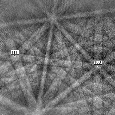
15 Properties of Kikuchi pattern 15 Each band : diffraction of a family of planes Intersections of bands : intersections of planes = zone axes Angles between bands : angles between planes Band widths : proportional to d(hkl) related to lattice parameters Middle line of a kikuchi band represents plane Excess line Zone axis Deficient line Kikuchi lines Kikuchi/EBSP pattern at a point
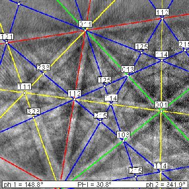
16 Indexing: Identifying various planes 16 Look Up Table (LUT) The angles between these bands formed by planes are measured from the Kikuchi pattern These values are compared against theoretical values of all angles formed by various planes for a given crystal system When the h-k-l values of a pair of lines are identified, it gives information about the pair of planes, but this does not distinguish between the two planes and hence this alone cannot be used to identify the orientation of the sample At least 3 sets of lines are required to completely identify the individual planes and hence find the orientation of the sample, as shown in Figure Angle (hkl) 1 (hkl)
17 Band Identification: Image processing 17

18 Hough Transform 18

19 Hough Transform 19

20 Hough Transform 20

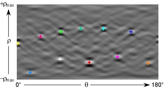
21 Hough Transform 21
22 EBSD Analysis 22
23 In order to specify an orientation, it is necessary to set up terms of reference, each of which is known as a coordinate system There are two coordinate systems: Sample (specimen) coordinate system Crystal coordinate system Coordinate systems 23 Specimen coordinate system: Coordinate system chosen as the geometry of the sample Crystal coordinate system: Coordinate system based on crystal orientation. In general [100], [010], [001] are adopted V. Randle et. al., 2000
24 24 orientation is then defined as 'the position of the crystal coordinate system with respect to the specimen coordinate system', i.e. where Cc and CS are the crystal and specimen coordinate systems respectively and g is the orientation matrix The fundamental means for expressing g is the rotation or orientation matrix The first row of the matrix is given by the cosines of the angles between the first crystal axis, [l00], and each of the three specimen axes, X, Y, Z, in turn In general sample coordinate system is the reference system


25 Orientation Maps 25 =100 µm; IPF; Step=1 µm; Grid300x200 =100 µm; BC; Step=1 µm; Grid300x200 Inverse Pole Figure Image Quality Map

26 Phase Maps 26 Titanium Aluminate Alumina Erbium Oxide Zirconium Oxide

27 Various kinds of boundaries 27
28 Charts: Misorientation Angle Distribution 28

29 Charts: Misorientation Profile 29
 is calculated from the area (A) assuming the grain is a circle: D")
30 Charts: Grain Size 30 The area (A) of a grain is the number (N) of points in the grain multiplied by a factor of the step size (s). For square grids: A = Ns 2 For hexagonal grids: A = N 3/2s 2 The diameter (D) is calculated from the area (A) assuming the grain is a circle: D = (4A/p) 1/2.
31 Pole Figures Consider a cubic crystal in a rolled sheet sample with "laboratory" or "sample" axes as shown below. 31 The Pole Figure plots the orientation of a given plane normal (pole) with respect to the sample reference frame. The example below is a (001) pole figure. Note the three points shown in the pole figure are for three symmetrically equivalent planes in the crystal.

32 Pole Figure: Texture Analysis 32
33 Orientation Distribution Function (ODF) 33 Although an orientation can be uniquely defined by a single point in Euler space, 3D graphs are hard to interpret Therefore ODF is a 2D representation of Euler Space Euler Space is divided into slices with interval of 5 o aluminum.matter.org.uk Slices arranged in gird called ODF
34 t-ebsd 34


35 SEM EBSD analysis of the microstructure in 316L chips formed with both the 0 and 20o raking angle 20 o tool angle: g = 1.5 not indexable a=+20 0 o tool angle: g = 1.9 a=0 tool indexable Large areas where the orientation cannot be determined (by indexing of Kikuchi patterns) 1. Due to refinement of the microstructure beyond the resolution limit of the SEM 2. Introduction of large amounts of colddeformation strain => decreasing the quality of the Kikuchi pattern Nothing could be indexed G. Facco; S. Shashank; M.R. Shankar; A.K. Kulovits; J.M.K. Wiezorek, MRS2010 Boston


36 G. Facco; S. Shashank; M.R. Shankar; A.K. Kulovits; J.M.K. Wiezorek, MRS2010 Boston TEM based OIM Analysis (+20 rake) 0.4 m 0.4 m 0.4 m 0.4 m Orientation spread 0.2 m 1. BF images show the formation of dislocation walls sub cell structure typical of large amounts of plastic deformation facilitated by conventional plastic deformation 2. OIM imaging shows large grains that contain low angle mis-orientations 3. OIM observations are consistent with BF image contrast of the dislocation wall sub cell structure


37 G. Facco; S. Shashank; M.R. Shankar; A.K. Kulovits; J.M.K. Wiezorek, MRS2010 Boston TEM based OIM Analysis (0 rake) 0.4 m 0.4 m 0.4 m 0.4 m 1. OIM imaging shows much smaller grains separated by High Angle Grain Boundaries HAGB s => grain refinement took place 2. 0 raking constitutes a severe plastic deformation process
38 Cross-correlation technique to determine elastic strain 38
 90min (f) 120min N. Sharma, S. Shashank; submitted to J.")
39 In-situ Recrystallization 39 (a) 26R (b) 500 C (c) 15min (d) 30min (e) 90min (f) 120min N. Sharma, S. Shashank; submitted to J. Microscopy


40 Band Contrast Intensity as userindependent parameter 40 N. Sharma, S. Shashank; submitted to J. Microscopy
")
 450 C. N.")

41 Recovery Parameter 41 (a) 26R, (b) 200 C and (c) 450 C. N. Sharma, S. Shashank; submitted to J. Microscopy


42 MAD as user-independent parameter 42 N. Sharma, S. Shashank; submitted to J. Microscopy
43 Summary EBSD is a very powerful technique for quantitative microscopy It is based on diffraction and hence can be used for any crystalline materials This method provides trove of data related to orientation, misorientation and can be extrapolated to represent strains, extent of recovery, recrystallization and may more things 43
EBSD Basics EBSD. Marco Cantoni 021/ Centre Interdisciplinaire de Microscopie Electronique CIME. Phosphor Screen. Pole piece.
 EBSD Marco Cantoni 021/693.48.16 Centre Interdisciplinaire de Microscopie Electronique CIME EBSD Basics Quantitative, general microstructural characterization in the SEM Orientation measurements, phase
EBSD Electron BackScatter Diffraction Principle and Applications
 EBSD Electron BackScatter Diffraction Principle and Applications Dr. Emmanuelle Boehm-Courjault EPFL STI IMX Laboratoire de Simulation des Matériaux LSMX emmanuelle.boehm@epfl.ch 1 Outline! Introduction!
Crystallographic orientation
 Crystallographic orientation Orientations and misorientations Orientation (g): The orientation of the crystal lattice with respect to some reference frame; usual a frame defined by the processing or sample
Carnegie Mellon MRSEC
 Carnegie Mellon MRSEC Texture, Microstructure & Anisotropy, Fall 2009 A.D. Rollett, P. Kalu 1 ELECTRONS SEM-based TEM-based Koseel ECP EBSD SADP Kikuchi Different types of microtexture techniques for obtaining
Strain. Two types of stresses: Usually:
 Stress and Texture Strain Two types of stresses: microstresses vary from one grain to another on a microscopic scale. macrostresses stress is uniform over large distances. Usually: macrostrain is uniform
AN INTRODUCTION TO OIM ANALYSIS
 AN INTRODUCTION TO OIM ANALYSIS Raising the standard for EBSD software The most powerful, flexible, and easy to use tool for the visualization and analysis of EBSD mapping data OIM Analysis - The Standard
ELECTRON BACKSCATTER DIFFRACTION (EBSD) THE METHOD AND ITS APPLICATIONS IN MATERIALS SCIENCE AND ENGINEERING
 THE METHOD AND ITS APPLICATIONS IN MATERIALS SCIENCE AND ENGINEERING") ELECTRON BACKSCATTER DIFFRACTION (EBSD) THE METHOD AND ITS APPLICATIONS IN MATERIALS SCIENCE AND ENGINEERING P. Cizek UNIVERSITY OF OXFORD, Department of Materials, Parks Road, Oxford OX1 3PH, GB Abstract
ELECTRON BACKSCATTER DIFFRACTION (EBSD) THE METHOD AND ITS APPLICATIONS IN MATERIALS SCIENCE AND ENGINEERING P. Cizek UNIVERSITY OF OXFORD, Department of Materials, Parks Road, Oxford OX1 3PH, GB Abstract
ORIENTATION DETERMINATION BY EBSP IN AN ENVIRONMENTAL SCANNING ELECTRON MICROSCOPE
 Pergamon PII S1359-6462(99)00086-X Scripta Materialia, Vol. 41, No. 1, pp. 47 53, 1999 Elsevier Science Ltd Copyright 1999 Acta Metallurgica Inc. Printed in the USA. All rights reserved. 1359-6462/99/$
3D-EBSD an CrossBeam-Systemen
 FIB- Workshop 3.-4. July 2008 3D-EBSD an CrossBeam-Systemen Ulrike Zeile 1, Ali Gholinia 2 and Frank Bauer 3 Arbeitskreis FIB SSOM DGM/DGE ASEM Hotel Seeburg, Luzern, Switzerland 1. Carl Zeiss NTS 2. Oxford
A Quantitative Evaluation of Microstructure by Electron Back-Scattered Diffraction Pattern Quality Variations
 Microsc. Microanal. 19, S5, 83 88, 2013 doi:10.1017/s1431927613012397 A Quantitative Evaluation of Microstructure by Electron Back-Scattered Diffraction Pattern Quality Variations SukHoonKang, 1 Hyung-Ha
Application of ASTAR/precession electron diffraction technique to quantitatively study defects in nanocrystalline metallic materials
 Graduate Theses and Dissertations Iowa State University Capstones, Theses and Dissertations 2017 Application of ASTAR/precession electron diffraction technique to quantitatively study defects in nanocrystalline
In-situ Heating Characterisation Using EBSD
 Webinar In-situ Heating Characterisation Using EBSD Speakers Dr. Ali Gholinia Dr. Neil Othen Dr. Jenny Goulden Topics Introduction to EBSD Why do in-situ experiments? EBSD equipment requirements for in-situ
Appendix 1 TEXTURE A1.1 REPRESENTATION OF TEXTURE
 Appendix 1 TEXTURE The crystallographic orientation or texture is an important parameter describing the microstructure of a crystalline material. Traditionally, textures have been determined by x-ray diffraction
COMPARISON OF TEXTURE IN COPPER AND ALUMINUM THIN FILMS DETERMINED BY XRD AND EBSD *
 COMPARISON OF TEXTURE IN COPPER AND ALUMINUM THIN FILMS DETERMINED BY XRD AND EBSD * 201 J. Müller 1, D. Balzar 1,2, R.H. Geiss 1, D.T. Read 1, and R.R. Keller 1 1 Materials Reliability Division, National
The effect of different step-size on the visualization of crystallographic defects using SEM/EBSD technique
 Int. Jnl. of Multiphysics Volume 9 Number 1 2015 37 The effect of different step-size on the visualization of crystallographic defects using SEM/EBSD technique Yoshikazu HIGA*, Ken SHIMOJIMA and Takashi
Mambo is the perfect tool for viewing EBSD data in pole and inverse pole figures.
 Mambo Pole figure and inverse pole figure software The physical properties of many samples are dependent on the common alignment of particular crystallographic directions: one of the easiest ways to view
Stuart I. Wright EDAX-TSL, Draper, Utah
 Stuart I. Wright EDAX-TSL, Draper, Utah EBSD Probably the Best Measurement in the World Austin Day, Microscopy & Microanalysis, 11, 502-503 (2005) OIM 3D Introduction to EBSD 3D Data Acquisition Serial
NEMI Sn Whisker Modeling Group Part 2:Future Work
 NEMI Sn Whisker Modeling Group Part 2:Future Work IPC/NEMI Meeting Maureen Williams, NIST Irina Boguslavsky, NEMI Consultant November 7, 2002 New Orleans, LA Capabilities of NEMI Modeling Group NEMI Fundamental
Microstructural Controls on Trace Element Variability in Ore Minerals
 2 Microstructural Controls on Trace Element Variability in Ore Minerals Question: Does EBSD provide new insight into ore mineral microstructure and the chemical enrichment of elements in hydrothermal ore
In-situ Observation of Microstructure Change in Steel by EBSD
 NIPPON STEEL & SUMITOMO METAL TECHNICAL REPORT No. 114 MARCH 2017 Technical Report UDC 621. 785. 36 In-situ Observation of Microstructure Change in Steel by EBSD Masayuki WAKITA* Seiichi SUZUKI Abstract
Electron channelling contrast imaging (ECCI) an amazing tool for observations of crystal lattice defects in bulk samples
 an amazing tool for observations of crystal lattice defects in bulk samples") Electron channelling contrast imaging (ECCI) an amazing tool for observations of crystal lattice defects in bulk samples Stefan Zaefferer with contributions of N. Elhami, (general & steels) Z. Li F. Ram,
Electron channelling contrast imaging (ECCI) an amazing tool for observations of crystal lattice defects in bulk samples Stefan Zaefferer with contributions of N. Elhami, (general & steels) Z. Li F. Ram,
QUANTITATIVE MICROSTRUCTURE ANALYSIS OF DISPERSION STRENGTHENED Al-Al 4 C 3 MATERIAL BY EBSD TECHNIQUE
 Acta Metallurgica Slovaca, Vol. 16, 2010, No.2, p. 97-101 97 QUANTITATIVE MICROSTRUCTURE ANALYSIS OF DISPERSION STRENGTHENED Al-Al 4 C 3 MATERIAL BY EBSD TECHNIQUE M. Varchola, M. Besterci, K. Sülleiová
 LA-UR-01-3685 Approved for public release; distribution is unlimited. Title: USING A MULTI-DISCIPLINARY APPROACH, THE FIRST ELECTRON BACKSCATTERED KIKUCHI PATTERNS WERE CAPTURED FOR A PLUTONIUM ALLOY Author(s):
Three stages: Annealing Textures. 1. Recovery 2. Recrystallisation most significant texture changes 3. Grain Growth
 Three stages: Annealing Textures 1. Recovery 2. Recrystallisation most significant texture changes 3. Grain Growth Cold worked 85% Cold worked 85% + stress relieved at 300 C for 1 hr Cold worked 85% +
Crystallographic Textures Measurement
 Crystallographic Textures Measurement D. V. Subramanya Sarma Department of Metallurgical and Materials Engineering Indian Institute of Technology Madras E-mail: vsarma@iitm.ac.in Macrotexture through pole
Observation in the GB (Gentle Beam) Capabilities
 Capabilities") A field-emission cathode in the electron gun of a scanning electron microscope provides narrower probing beams at low as well as high electron energy, resulting in both improved spatial resolution and
A field-emission cathode in the electron gun of a scanning electron microscope provides narrower probing beams at low as well as high electron energy, resulting in both improved spatial resolution and
Liverpool, UK, L69 3GP
 Materials Science Forum Vols. 467-470 (2004) pp. 573-578 online at http://www.scientific.net 2004 Trans Tech Publications, Switzerland Using electron backscatter diffraction (EBSD) to measure misorientation
TEM and Electron Diffraction Keith Leonard, PhD (1999) U. Cincinnati
 U. Cincinnati") TEM and Electron Diffraction Keith Leonard, PhD (1999) U. Cincinnati Electron Microscopes: Electron microscopes, such as the scanning electron microscope (SEM) and transmission electron microscope (TEM)
TEM and Electron Diffraction Keith Leonard, PhD (1999) U. Cincinnati Electron Microscopes: Electron microscopes, such as the scanning electron microscope (SEM) and transmission electron microscope (TEM)
3. Anisotropic blurring by dislocations
 Dynamical Simulation of EBSD Patterns of Imperfect Crystals 1 G. Nolze 1, A. Winkelmann 2 1 Federal Institute for Materials Research and Testing (BAM), Berlin, Germany 2 Max-Planck- Institute of Microstructure
Diffraction Going further
 Diffraction Going further Duncan Alexander! EPFL-CIME 1 Contents Higher order Laue zones (HOLZ)! Kikuchi diffraction! Convergent beam electron diffraction (CBED)! HOLZ lines in CBED! Thickness measurements!
Study of the Initial Stage and an Anisotropic Growth of Oxide Layers Formed on Zircaloy-4
 16 th International Symposium on Zirconium in the Nuclear Industry, Chengdu, P. R. China, May 10-13, 2010 Study of the Initial Stage and an Anisotropic Growth of Oxide Layers Formed on Zircaloy-4 B. X.
Advances in EBSD Analysis Using Novel Dynamical Pattern Simulation Software
 Advances in EBSD Analysis Using Novel Dynamical Pattern Simulation Software Bruker Nano GmbH, Berlin Webinar, November 5 th, 2014 Innovation with Integrity Presenters Dr. Daniel Goran Product Manager EBSD,
11.3 The analysis of electron diffraction patterns
 11.3 The analysis of electron diffraction patterns 277 diameter) Ewald reflecting sphere, the extension of the reciprocal lattice nodes and the slight buckling of the thin foil specimens all of which serve
Microstructure Evolution of Polycrystalline Pure Nickel during Static Recrystallization 1
 Materials Transactions, Vol. 43, No. 9 (2002) pp. 2243 to 2248 c 2002 The Japan Institute of Metals Microstructure Evolution of Polycrystalline Pure Nickel during Static Recrystallization 1 Makoto Hasegawa
Single crystal X-ray diffraction. Zsolt Kovács
 Single crystal X-ray diffraction Zsolt Kovács based on the Hungarian version of the Laue lab description which was written by Levente Balogh, Jenő Gubicza and Lehel Zsoldos INTRODUCTION X-ray diffraction
Grain Contrast Imaging in UHV SLEEM
 Materials Transactions, Vol. 51, No. 2 (2010) pp. 292 to 296 Special Issue on Development and Fabrication of Advanced Materials Assisted by Nanotechnology and Microanalysis #2010 The Japan Institute of
Microstructure and texture of asymmetrically rolled aluminium and titanium after deformation and recrystallization
 IOP Conference Series: Materials Science and Engineering PAPER OPEN ACCESS Microstructure and texture of asymmetrically rolled aluminium and titanium after deformation and recrystallization To cite this
Practical 2P8 Transmission Electron Microscopy
 Practical 2P8 Transmission Electron Microscopy Originators: Dr. N.P. Young and Prof. J. M. Titchmarsh What you should learn from this practical Science This practical ties-in with the lecture course on
Electron backscatter diffraction (EBSD) in the SEM: applications to microstructures in minerals and rocks and recent technological advancements
 in the SEM: applications to microstructures in minerals and rocks and recent technological advancements") Electron backscatter diffraction (EBSD) in the SEM: applications to microstructures in minerals and rocks and recent technological advancements Elisabetta Mariani a, D. J. Prior a, D. McNamara a, M. A.
Electron backscatter diffraction (EBSD) in the SEM: applications to microstructures in minerals and rocks and recent technological advancements Elisabetta Mariani a, D. J. Prior a, D. McNamara a, M. A.
On-axis Transmission Kikuchi Diffraction in the SEM. Performances and Applications
 On-axis Transmission Kikuchi Diffraction in the SEM. Performances and Applications Etienne Brodu, Emmanuel Bouzy, Jean-Jacques Fundenberger Séminaire «les microscopies électroniques à Metz et à Nancy»
EFFECT OF CRYSTALLOGRAPHIC ORIENTATION ON MECHANICAL PROPERTIES OF STEEL SHEETS BY DEPTH SENSING INDENTATION
 EFFECT OF CRYSTALLOGRAPHIC ORIENTATION ON MECHANICAL PROPERTIES OF STEEL SHEETS BY DEPTH SENSING INDENTATION Peter BURIK 1, Ladislav PEŠEK 2 1 Technical University of Liberec, Faculty of Mechanical Engineering,
Determining the Dependence of Grain Boundary Mobility on Misorientation in High Purity Aluminum with Zirconium Additions. A Thesis
 Determining the Dependence of Grain Boundary Mobility on Misorientation in High Purity Aluminum with Zirconium Additions A Thesis Submitted to the Faculty of Drexel University by David J. Shields in partial
Finding Grain and Antigrains. Matt Nowell May 2016
 Finding Grain and Antigrains Matt Nowell May 2016 1 Grains Grain Boundaries Grain Size Measurements Special Boundaries Grain Shape Antigrains Outline Acknowledgements Stuart Wright, Rene de Kloe (EDAX),
Electron Microscopy Studies of Niobium Thin Films on Copper
 Electron Microscopy Studies of Niobium Thin Films on Copper Roy Crooks 1, Greg Thompson 2, Robb Morris 2, Michelle Adams Hughes 3, Daudi Waryoba 3, and Peter Kalu 3 1 Black Laboratories, L.L.C., Newport
TEM imaging and diffraction examples
 TEM imaging and diffraction examples Duncan Alexander EPFL-CIME 1 Diffraction examples Kikuchi diffraction Epitaxial relationships Polycrystalline samples Amorphous materials Contents Convergent beam electron
Characterization of Al-8090 superplastic materials using orientation imaging microscopy
 Materials Science and Engineering A242 (1998) 284 291 Characterization of Al-8090 superplastic materials using orientation imaging microscopy H. Garmestani a, *, P. Kalu a, D. Dingley 1,b a FAMU/FSU College
LECTURE 7. Dr. Teresa D. Golden University of North Texas Department of Chemistry
 LECTURE 7 Dr. Teresa D. Golden University of North Texas Department of Chemistry Diffraction Methods Powder Method For powders, the crystal is reduced to a very fine powder or microscopic grains. The sample,
Crystallographic Distribution of Low Angle Grain Boundary Planes in Magnesium Oxide
 Citation & Copyright (to be inserted by the publisher ) Crystallographic Distribution of Low Angle Grain Boundary Planes in Magnesium Oxide D.M. Saylor 1, A. Morawiec 2, K.W. Cherry 1, F.H. Rogan 1, G.S.
Symmetry and Anisotropy Structure, Properties, Sample and Material, Texture and Anisotropy, Symmetry
 Symmetry and Anisotropy Structure, Properties, Sample and Material, Texture and Anisotropy, Symmetry Objectives Symmetry Operators & Matrix representation. Effect of crystal and sample symmetry
Investigating the crystal orientation of SiC CVD using orientation imaging microscopy (OIM) & X-ray diffraction (XRD) by Deepak Ravindra
 & X-ray diffraction (XRD) by Deepak Ravindra") Investigating the crystal orientation of SiC CVD using orientation imaging microscopy (OIM) & X-ray diffraction (XRD) by Deepak Ravindra Project Details SiC coating is ~200 microns thick on SiC substrate
Investigating the crystal orientation of SiC CVD using orientation imaging microscopy (OIM) & X-ray diffraction (XRD) by Deepak Ravindra Project Details SiC coating is ~200 microns thick on SiC substrate
Changes in Microstructure of Al/AlN Interface during Thermal Cycling
 Materials Transactions, Vol. 49, No. 12 (2008) pp. 2808 to 2814 #2008 The Japan Institute of Metals Changes in Microstructure of / Interface during Thermal Cycling Yoshiyuki Nagatomo 1, Takeshi Kitahara
Applications of EBSD
 Applications of EBSD Dr. V. Subramanya Sarma Department of Metallurgical and Materials Engineering Indian Institute of Technology Madras E-mail: vsarma@iitm.ac.in Applications of EBSD Grain size distribution
Practical 2P8 Transmission Electron Microscopy
 Practical 2P8 Transmission Electron Microscopy Originators: Dr. M. L. Jenkins and Prof. J. M. Titchmarsh What you should learn from this practical Science This practical ties-in with the lecture course
Empirical constraints of shock features in monazite using shocked zircon inclusions
 GSA Data Repository 2016205 Empirical constraints of shock features in monazite using shocked zircon inclusions Erickson et al. DR 1 Analytical methods Identification of Shocked Monazites and Imaging External
TEM imaging and diffraction examples
 TEM imaging and diffraction examples Duncan Alexander EPFL-CIME 1 Diffraction examples Kikuchi diffraction Epitaxial relationships Polycrystalline samples Amorphous materials Contents Convergent beam electron
Electron Microscopy. Dynamical scattering
 Electron Microscopy 4. TEM Basics: interactions, basic modes, sample preparation, Diffraction: elastic scattering theory, reciprocal space, diffraction pattern, Laue zones Diffraction phenomena Image formation:
Imaging with Diffraction Contrast
 Imaging with Diffraction Contrast Duncan Alexander EPFL-CIME 1 Introduction When you study crystalline samples TEM image contrast is dominated by diffraction contrast. An objective aperture to select either
MICROSTRUCTURAL STABILITY OF ULTRAFINE GRAINED COPPER AT ELEVATED TEMPERATURE
 Acta Metallurgica Slovaca, Vol. 17, 2011, No. 3, p. 158-162 158 MICROSTRUCTURAL STABILITY OF ULTRAFINE GRAINED COPPER AT ELEVATED TEMPERATURE L. Pantělejev 1, O. Man 1, L. Kunz 2 1 Brno University of Technology,
Influence of Crystal Orientations on the Bendability of an Al-Mg-Si Alloy
 Materials Transactions, Vol. 51, No. 4 (2010) pp. 614 to 619 Special Issue on Crystallographic Orientation Distribution and Related Properties in Advanced Materials II #2010 The Japan Institute of Light
Evolution of Microstructure and Texture Associated with Ridging in Ferritic Stainless Steels
 , pp. 100 105 Evolution of Microstructure and Texture Associated with Ridging in Ferritic Stainless Steels SooHo PARK, KwangYuk KIM, YongDeuk LEE and ChanGyung PARK 1) Stainless Steel Research Group, Technical
STUDIES ON THE ACCURACY OF ELECTRON BACKSCATTER DIFFRACTION MEASUREMENTS
 STUDIES ON THE ACCURACY OF ELECTRON BACKSCATTER DIFFRACTION MEASUREMENTS Melik C. Demirel, Bassem S. El-Dasher, Brent L. Adams, and Anthony D. Rollett Materials Science & Engineering Department Carnegie
EMSE Weak-Beam Dark-Field Technique
 Weak-Beam Dark-Field Technique 1 Weak-Beam Dark-Field Imaging Basic Idea recall bright-field contrast of dislocations: specimen close to Bragg condition, s î 0 near the dislocation core, some planes curved
Kinematical theory of contrast
 Kinematical theory of contrast Image interpretation in the EM the known distribution of the direct and/or diffracted beam on the lower surface of the crystal The image on the screen of an EM = the enlarged
MICROSTRUCTURE CHARACTERIZATION OF GOES AFTER HOT ROLLING AND COLD ROLLING + DECARBURIZATION ANNEALING
 MICROSTRUCTURE CHARACTERIZATION OF GOES AFTER HOT ROLLING AND COLD ROLLING + DECARBURIZATION ANNEALING Vlastimil VODÁREK 1, Jan HOLEŠINSKÝ 1, Anastasia MASLOVA 1, František FILUŠ 1, Šárka MIKLUŠOVÁ 2,
Analyses on Compression Twins in Magnesium
 aterials Transactions, Vol. 49, No. 4 (2008) pp. 710 to 714 #2008 The Japan Institute of etals Analyses on Compression Twins in agnesium L. eng 1, P. Yang 1; *, Q. Xie 1 and W. ao 1;2 1 School of aterials
LSPM CNRS, Université Paris 13, 99 av. J.B. Clément, Villetaneuse, France
 Advanced Materials Research Online: 2014-08-11 ISSN: 1662-8985, Vol. 996, pp 106-111 doi:10.4028/www.scientific.net/amr.996.106 2014 Trans Tech Publications, Switzerland Modeling methodology for stress
EBSD Introduction 1. Electron BackScatter Diffraction - basics and applications - René de Kloe EDAX BV, Tilburg, The Netherlands.
 Electron BackScatter Diffraction - basics and applications - René de Kloe EDAX BV, Tilburg, The Netherlands Stuart Wright, Matt Nowell, John Carpenter EDAX-TSL, Draper, Utah Outline OIM or orientation
Risks of Cleaning Electron Backscatter Diffraction Data
 Risks of Cleaning Electron Backscatter Diffraction Data L.N. Brewer* and J.R. Michael Sandia National Laboratories, P.O. Box 5800, Albuquerque, NM 87185 * lnbrewe@sandia.gov Introduction Collecting good
MTEX. an open source texture analysis toolbox. Ralf Hielscher. Belo Horizonte, TU Chemnitz, Germany
 MTEX an open source texture analysis toolbox Ralf Hielscher TU Chemnitz, Germany Belo Horizonte, 2015 What is MTEX? 1 a MATLAB toolbox for quantitative texture analysis 2 a scripting language 3 a tool
University of Groningen. Dynamics of tempering processes in stainless steel De Jeer, Leo T.H.; Ocelik, Vaclav; De Hosson, J.T.M.
 University of Groningen Dynamics of tempering processes in stainless steel De Jeer, Leo T.H.; Ocelik, Vaclav; De Hosson, J.T.M. Published in: WIT Transactions on Engineering Sciences DOI: 10.2495/MC170191
ARTICLE IN PRESS. Ultramicroscopy
 Ultramicroscopy 109 (2009) 1148 1156 Contents lists available at ScienceDirect Ultramicroscopy journal homepage: www.elsevier.com/locate/ultramic Bragg s Law diffraction simulations for electron backscatter
Structural change during cold rolling of electrodeposited copper
 Materials Science Forum Vols. 539-543 (2007) pp. 5013-5018 online at http://www.scientific.net (2007) Trans Tech Publications, Switzerland Structural change during cold rolling of electrodeposited copper
Diffraction Contrast Tomography. Unlocking Crystallographic Information from Laboratory X-ray Microscopy. Technical Note
 Diffraction Contrast Tomography Unlocking Crystallographic Information from Laboratory X-ray Microscopy Technical Note Diffraction Contrast Tomography Unlocking Crystallographic Information from Laboratory
Application of Scanning Electron Microscope to Dislocation Imaging in Steel
 Application of Scanning Electron Microscope to Dislocation Imaging in Steel Masaaki Sugiyama and Masateru Shibata Advanced Technology Research Laboratories, Nippon Steel Corporation SM Business Unit, JEOL
Electron microscopy II
 Electron microscopy II Nanomaterials characterization I RNDr. Věra Vodičková, PhD. Interaction ction: electrons solid matter Signal types SE.secondary e - AE Auger s e - BSE back scattered e - X-ray photons,
Microstructure of Friction Stir Welded 6061 Aluminum Alloy
 Proceedings of the 9 th International Conference on Aluminium Alloys (2004) Edited by J.F. Nie, A.J. Morton and B.C. Muddle Institute of Materials Engineering Australasia Ltd 878 Microstructure of Friction
LaboTex Version 3.0. Texture Analysis Software for Windows. Texture Analysis on the Basis of EBSD Data
 LaboTex Version 3.0 Texture Analysis Software for Windows Texture Analysis on the Basis of EBSD Data LaboSoft s.c. Telephone: +48 502 311 838 Fax: +48 12 3953 891 E-mail: office@labosoft.com.pl LaboSoft
Development of bimodal grain structures in microalloyed steels:
 Development of bimodal grain structures in microalloyed steels: Niobium and titanium are added to high strength low alloy (HSLA) steels to provide grain boundary pinning precipitates to help produce the
STUDY & ANALYSIS OF ALUMINIUM FOIL AND ANATASE TITANIUM OXIDE (TiO2) USING TRANSMISSION ELECTRON MICROSCOPY
 USING TRANSMISSION ELECTRON MICROSCOPY") STUDY & ANALYSIS OF ALUMINIUM FOIL AND ANATASE TITANIUM OXIDE (TiO2) USING TRANSMISSION ELECTRON MICROSCOPY Ayush Garg Department of Chemical and Materials Engineering, University of Auckland, Auckland,
STUDY & ANALYSIS OF ALUMINIUM FOIL AND ANATASE TITANIUM OXIDE (TiO2) USING TRANSMISSION ELECTRON MICROSCOPY Ayush Garg Department of Chemical and Materials Engineering, University of Auckland, Auckland,
The object of this experiment is to test the de Broglie relationship for matter waves,
 Experiment #58 Electron Diffraction References Most first year texts discuss optical diffraction from gratings, Bragg s law for x-rays and electrons and the de Broglie relation. There are many appropriate
Texture Analysis using OIM
 Texture Analysis using OIM Stuart I. Wright Acknowledgements: David Field, Washington State University Karsten Kunze, ETH Zurich Outline What is crystallographic texture? Mathematical constructs Texture
SI GUIDE. File Name: Supplementary Information Description: Supplementary Figures, Supplementary Notes and Supplementary References.
 SI GUIDE File Name: Supplementary Information Description: Supplementary Figures, Supplementary Notes and Supplementary References. File Name: Supplementary Movie 1 Description: (the movie from which Figs.
Effects of Grain Size and Orientation on Mechanical Response of Lead Free Solders. Jing Zou
 Effects of Grain Size and Orientation on Mechanical Response of Lead Free Solders by Jing Zou A thesis submitted to the Graduate Faculty of Auburn University in partial fulfillment of the requirements
ORIENTATION DEPENDENCE OF DISLOCATION STRUCTURE EVOLUTION OF ALUMINUM ALLOYS IN 2-D AND 3-D COLIN CLARKE MERRIMAN
 ORIENTATION DEPENDENCE OF DISLOCATION STRUCTURE EVOLUTION OF ALUMINUM ALLOYS IN 2-D AND 3-D By COLIN CLARKE MERRIMAN A thesis submitted in partial fulfillment of the requirements for the degree of: MASTER
MICROSTRUCTURE AND MECHANICAL PROPERTIES OF POWDER ALUMINIUM PREPARED BY SEVERE PLASTIC DEFORMATION
 MICROSTRUCTURE AND MECHANICAL PROPERTIES OF POWR ALUMINIUM PREPARED BY SEVERE PLASTIC FORMATION Jiří DVOŘÁK 1a, Petr KRÁL 2a, Martin BALOG 3b, František SIMANČÍK 4b, Václav SKLENIČKA 5a a Institute of
Deformation Microstructure and Texture in a Cold-Rolled Austenitic Steel with Low Stacking-Fault Energy
 Materials Transactions, Vol. 51, No. 4 (2010) pp. 620 to 624 Special Issue on Crystallographic Orientation Distribution and Related Properties in Advanced Materials II #2010 The Japan Institute of Metals
Diffraction Basics. The qualitative basics:
 The qualitative basics: Diffraction Basics Coherent scattering around atomic scattering centers occurs when x-rays interact with material In materials with a crystalline structure, x-rays scattered in
INFLUENCE OF MICROSTRUCTURE ON THE PROPAGATION OF FATIGUE CRACKS IN INCONEL 617. Benjiman Michael Albiston. A thesis. submitted in partial fulfillment
 INFLUENCE OF MICROSTRUCTURE ON THE PROPAGATION OF FATIGUE CRACKS IN INCONEL 617 by Benjiman Michael Albiston A thesis submitted in partial fulfillment of the requirements for the degree of Master of Science
Characteristics of an Aluminum Alloy after Generation of Fine Grains Using Equal Channel Angular Extrusion Process
 Journal of Emerging Trends in Engineering and Applied Sciences (JETEAS) 2 (2): 289-293 Scholarlink Research Institute Journals, 2011 (ISSN: 2141-7016) jeteas.scholarlinkresearch.org Journal of Emerging
Thin Film Scattering: Epitaxial Layers
 Thin Film Scattering: Epitaxial Layers 6th Annual SSRL Workshop on Synchrotron X-ray Scattering Techniques in Materials and Environmental Sciences: Theory and Application May 29-31, 2012 Thin films. Epitaxial
Investigation of SIBM driven recrystallization in alpha Zirconium based on EBSD data and Monte Carlo modeling
 IOP Conference Series: Materials Science and Engineering PAPER OPEN ACCESS Investigation of SIBM driven recrystallization in alpha Zirconium based on EBSD data and Monte Carlo modeling To cite this article:
Effects of Wavy Roll-Forming on Textures in AZ31B Magnesium Alloy
 Materials Transactions, Vol. 49, No. 5 (8) pp. 995 to 999 Special Issue on Platform Science and Technology for Advanced Magnesium Alloys, IV #8 The Japan Institute of Metals Effects of Wavy Roll-Forming
Arch. Metall. Mater. 62 (2017), 2B,
, 2B,") Arch. Metall. Mater. 62 (2017), 2B, 1243-1248 DOI: 10.1515/amm-2017-0185 S.-W. KIM* #, T.-Y. AHN*, Y.-S. LIM*, S.-S. HWANG* EFFECT OF LOCAL STRAIN DISTRIBUTION OF COLD-ROLLED ALLOY 690 ON PRIMARY WATER
Arch. Metall. Mater. 62 (2017), 2B, 1243-1248 DOI: 10.1515/amm-2017-0185 S.-W. KIM* #, T.-Y. AHN*, Y.-S. LIM*, S.-S. HWANG* EFFECT OF LOCAL STRAIN DISTRIBUTION OF COLD-ROLLED ALLOY 690 ON PRIMARY WATER
Representation of Orientation
 Representation of Orientation Lecture Objectives - Representation of Crystal Orientation Stereography : Miller indices, Matrices 3 Rotations : Euler angles Axis/Angle : Rodriques Vector, Quaternion - Texture
Homework 6: Calculation of Misorientation; A.D. Rollett, , Texture, Microstructure and Anisotropy
 Homework 6: Calculation of Misorientation; A.D. Rollett, 27-75, Texture, Microstructure and Anisotropy Due date: 8 th November, 211 Corrected 8 th Nov. 211 Q1. [6 points] (a) You are given a list of orientations
Analysis of EBSD Data
 Analysis of EBSD Data 27-750 Texture, Microstructure & Anisotropy B. El-Dasher*, A.D. Rollett, M.H. Alvi, G.S. Rohrer, P.N. Kalu 1, T. Bennett 2, N. Bozzolo 3 and F. Wagner 4 *formerly at Lawrence Livermore
Recrystallization Theoretical & Practical Aspects
 Theoretical & Practical Aspects 27-301, Microstructure & Properties I Fall 2006 Supplemental Lecture A.D. Rollett, M. De Graef Materials Science & Engineering Carnegie Mellon University 1 Objectives The
Microstructural Characterization of Materials
 Microstructural Characterization of Materials 2nd Edition DAVID BRANDON AND WAYNE D. KAPLAN Technion, Israel Institute of Technology, Israel John Wiley & Sons, Ltd Contents Preface to the Second Edition
{001} Texture Map of AA5182 Aluminum Alloy for High Temperature Uniaxial Compression
 Materials Transactions, Vol., No. (00) pp. 6 to 67 #00 The Japan Institute of Light Metals {00} Texture Map of AA8 Aluminum Alloy for High Temperature Uniaxial Compression Hyeon-Mook Jeong*, Kazuto Okayasu
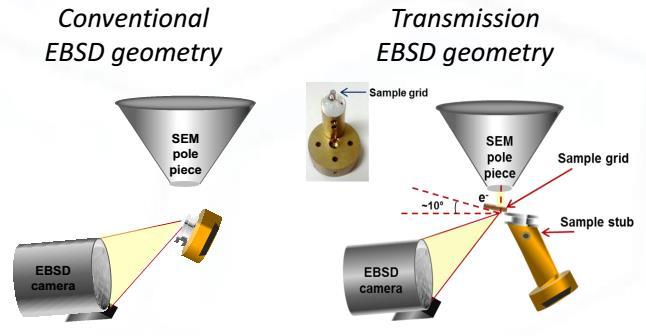
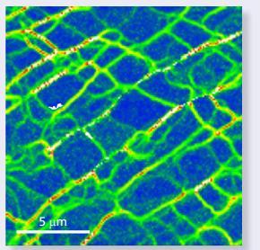
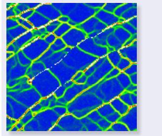
Transmission Kikuchi Diffraction in the Scanning Electron Microscope
 Transmission Kikuchi Diffraction in the Scanning Electron Microscope Robert Keller, Roy Geiss, Katherine Rice National Institute of Standards and Technology Nanoscale Reliability Group Boulder, Colorado