Motorola PC603R Microprocessor
|
|
|
- Jared Stephens
- 6 years ago
- Views:
Transcription
1 Construction Analysis Motorola PC603R Microprocessor Report Number: SCA Global Semiconductor Industry the Serving Since N. Hartford Drive Scottsdale, AZ Phone: Fax: Internet:
2 INDEX TO TEXT TITLE PAGE INTRODUCTION 1 MAJOR FINDINGS 1 TECHNOLOGY DESCRIPTION Assembly 2 Die Process 2-3 ANALYSIS RESULTS Die Process and Design 4-7 ANALYSIS PROCEDURE 8 TABLES Overall Evaluation 9 Package Markings 10 Die Material Analysis 10 Horizontal Dimensions 11 Vertical Dimensions 12 - i -
3 INTRODUCTION This report describes a construction analysis of the Motorola PC603R Microprocessor. Two engineering samples were supplied for the analysis. The devices were received in 256-pin Ball Grid Array (BGA) packages date coded MAJOR FINDINGS Questionable Items: 1 Significant misalignment of metal 2 and 4 to the underlying plugs was noted (Figures 19 and 29) Special Features: Six metal, P-epi, BiCMOS process. Metal 1 (tungsten) was defined by a damascene process. Stacked vias were employed. Chemical-mechanical-planarization (CMP). Oxide-filled shallow-trench isolation. Titanium silicided diffusion structures. Aggressive design rule features (0.2 micron gates). 1 These items present possible quality or reliability concerns. They should be discussed with the manufacturer to determine their possible impact on the intended application
4 TECHNOLOGY DESCRIPTION Assembly: The devices were packaged in 256-pin (255 actual pins) Ball Grid Arrays (BGAs). The die was mounted surface down on the ceramic substrate (C4 flip-chip assembly). A blue colored underfill was present between the die surface and the ceramic substrate. Solder balls were employed for all connections to die metallization (C4 flip-chip process). There appeared to be space for standard bond pads around the die perimeter although used for protection diodes (?) in this case (see Figure 6). Sawn dicing (full depth). Die Process: Fabrication process: Oxide-filled shallow-trench isolation, BiCMOS process employing twin-wells in an apparent P-epi on a P substrate. Die coat: A thin patterned polyimide die coat was present over the entire die. Final passivation: A layer of nitride over a layer of glass. Metallization: Six levels of metal defined by standard dry-etch techniques (except M1). Metal 1 (tungsten) was defined by a damascene process. Metals 2-6 consisted of aluminum. Metal 6 did not employ a cap or barrier metal. Metals 2-5 employed titanium-nitride caps and barriers. Tungsten plugs were employed for vias under metals 2-5. Metal 6 used standard vias. All tungsten plugs and tungsten metal 1 were lined with titanium-nitride. Stacked vias were employed at all levels. Elongated vias (M6 - M3) and contacts (M1) were also present
5 TECHNOLOGY DESCRIPTION (continued) Interlevel dielectrics: Interlevel dielectric 5 (between M5 and M6) consisted of two layers of glass. The first layer was subjected to an etchback. Interlevel dielectrics 2-4 used the same dielectric structure. A very thin glass was deposited first, followed by three separate layers of glass. The third layer of glass was planarized by CMP which left the surface very planar. The fourth layer appeared to have been similarly planarized during tungsten plug CMP. Interlevel dielectric 1 (between M1 and M2) consisted of a single thick layer of glass which had also been subjected to CMP. Pre-metal glass: A thin layer of glass over a thick layer of glass and a thin nitride. This dielectric was also planarized by CMP. Polysilicon: A single layer of dry-etched polycide (poly and titanium-silicide). This layer was used to form all gates on the die. Nitride sidewall spacers were used to provide the LDD spacing. Diffusions: Implanted N+ and P+ diffusions formed the sources/drains of transistors. Titanium was sintered into the diffusions (salicide process). Isolation: Field oxide consisted of oxide-filled shallow-trench isolation. It was very planar with the diffused silicon surfaces. A small step was noted on top of the trench oxide at well boundaries. Wells: Twin-wells in a P-epi on a P substrate. SRAM: On-chip cache memory cell arrays were employed. The memory cells used a 6T CMOS SRAM cell design. Metal 3 formed the bit lines and metal 2 distributed GND and Vcc throughout the cells and was used as piggyback word lines and cell interconnect. Metal 1 also provided cell interconnect. Polycide formed the select and storage gates. Cell pitch was 3.5 x 5.1 microns (17.8 microns 2 ). There appeared to be bipolar devices on the die; however, we could not verify them in cross-section due to our inability to see them before complete delayering. No redundancy fuses were found
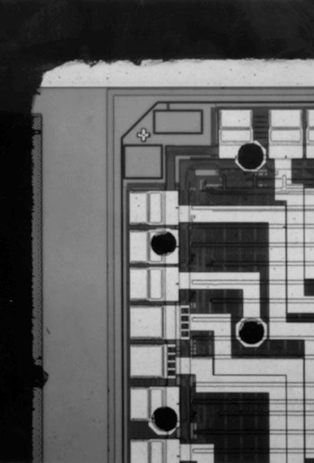
6 ANALYSIS RESULTS Die Process and Design : Figures 1-46 Questionable Items: 1 Significant misalignment of metal 2 and 4 to the underlying plugs was noted (Figures 19 and 29) Special Features: Six metal, P-epi, BiCMOS process. Metal 1 (tungsten) was defined by a damascene process. Stacked vias were employed. Chemical-mechanical-planarization (CMP). Oxide-filled shallow-trench isolation. Titanium silicided diffusion structures. Aggressive design rule features (0.2 micron). General items: Fabrication process: Oxide filled shallow-trench isolation, BiCMOS process employing twin-wells in an apparent P-epi on a P substrate. No problems were found in the process. Design implementation: Die layout was clean and efficient. Alignment was adequate at most levels; however, alignment of metals 2 and 4 to their respective underlying plugs was poor. Plug coverage was only 35-to-40 percent at some metal 2 and 4 vias. Some isolated metal 6 vias were noted on the die (see Figure 6). 1 These items present possible quality or reliability concerns. They should be discussed with the manufacturer to determine their possible impact on the intended application
7 ANALYSIS RESULTS (continued) Surface defects: No toolmarks, masking defects, or contamination areas were found. Die coat: A patterned polyimide die coat was present over the entire die surface. Final passivation: A layer of nitride over a layer of glass. Coverage was good. Edge seal was also good as the passivation extended to the scribe lane to seal the metallization. A cutout was present in the passivation and ILD 5 around the die perimeter to prevent cracks from radiating over the circuitry. Metallization: Six levels of metal interconnect. Metals 2-6 consisted of aluminum. Metals 2-5 employed titanium-nitride caps and barriers. Metal 6 did not employ a cap or barrier metal. Tungsten plugs were employed with metals 2-5. All plugs were lined with titanium-nitride underneath and over top. Standard vias were employed under metal 6. Metal 1 consisted of tungsten defined by a damascene process. The metal 1 tungsten was also lined with titaniumnitride. Metal patterning: All aluminum metal levels were defined by a dry etch of good quality. Metal lines were only widened at metal 6 via connections. Metal defects: None (excluding misalignment). No voiding, notching or cracking of the metal layers was found. No silicon nodules were found following removal of the metal layers. Metal step coverage: Metal 6 thinned up to 75 percent at vias. Although the thinning exceeds MIL-STDs (70 percent) it is not considered a reliability concern. No metal thinning was present at the connections to the tungsten via plugs or metal 1. The absence of thinning is due to the good control of plug height and the planarization technique employed. Vias and contacts: All via and contact cuts were defined by a dry etch of good quality. Again there was significant misalignment of metal 2 and 4 to their respective plugs. This misalignment reduced metal spacing to adjacent plugs (see Figure 32). Some tungsten plugs spilled over one edge of the metal. IBM uses this borderless contact technique for improved contact resistance. Vias and contacts were placed directly over one another (stacked vias). No problems were noted
8 ANALYSIS RESULTS (continued) Interlevel dielectrics: Interlevel dielectric 5 (between M5 and M6 ) consisted of two layers of glass. The first layer was subjected to an etchback. Interlevel dielectrics 2-4 consisted of the same type of oxide structure. A very thin glass was deposited first, followed by three separate layers of glass. The third and fourth layers of glass were subjected to CMP which left the surface very planar. No CMP was performed on ILD 5 (under M6). Interlevel dielectric 1 (between M2 and M1) consisted of a single thick layer of glass which had also been subjected to CMP. No problems were found with any of these layers. Pre-metal glass: A thin layer of silicon-dioxide over a thick layer of glass and a thin nitride. This layer was also planarized by chemical-mechanical-planarization. No problems were found. Polysilicon: A single level of polycide (poly and titanium-silicide) was used. It formed all gates and word lines in the array. Definition was by dry etch of good quality. Nitride sidewall spacers were used throughout and left in place. No problems were found. Isolation: The device used oxide-filled shallow-trench isolation which was quite planar with the silicon surface. A small step was noted on top of the trench oxide at well boundaries. No problems were present. Diffusions: Implanted N+ and P+ diffusions were used for sources and drains. Titanium was sintered into the diffusions (salicide process) to reduce series resistance. An LDD process was used employing nitride sidewall spacers. Wells: Twin-wells were used in a P-epi on a P substrate. Definition was normal. We could not delineate the P-well in cross-section. Buried contacts: Direct poly to diffusion contacts were not used. SRAM: As mentioned, on-chip cache memory cell arrays were employed on the device. The SRAM cell array used a 6T CMOS SRAM cell design. Metal 3 formed the bit lines. Metal 2 distributed GND and Vcc throughout the cells and was used as piggyback word lines and cell interconnect. Metal 1 also provided cell interconnect. Polycide formed the word lines/select and storage gates. Cell pitch was 3.5 x 5.1 microns
9 ANALYSIS RESULTS (continued) There appeared to also be bipolar devices on the die as observed from the surface. Since they could only be seen once the die was delayered we were unsuccessful in obtaining a cross section through one of these devices to observe the sectional structure. No redundancy fuses were noted
10 PROCEDURE The devices were subjected to the following analysis procedures: External inspection X-ray Die optical inspection Delayer to metal 6 and inspect Aluminum removal (metal 6) Delayer to metal 5 and inspect Aluminum removal (metal 5) and inspect tungsten plugs Delayer to metal 4 and inspect Aluminum removal (metal 4) and inspect tungsten plugs Delayer to metal 3 and inspect Aluminum removal (metal 3) and inspect tungsten plugs Delayer to metal 2 and inspect Aluminum removal (metal 2) and inspect tungsten plugs Delayer to metal 1 and inspect Tungsten removal (metal 1) Delayer to polycide/substrate and inspect Die sectioning (90 for SEM) Measure horizontal dimensions Measure vertical dimensions Die material analysis - 8 -
11 OVERALL QUALITY EVALUATION : Overall Rating: Normal. DETAIL OF EVALUATION Package integrity Package markings Die placement Solder ball placement Solder ball interconnect quality Dicing quality Die attach quality Die attach method Dicing method G G G G G N G C4 solder ball interconnect technique Sawn Die surface integrity: Toolmarks (absence) G Particles (absence) G Contamination (absence) G Process defects (absence) G General workmanship G Passivation integrity G Metal definition G Metal integrity N Metal registration NP 1 Contact coverage NP 1 Via/contact registration N Etch control (depth) N 1 Misalignment of M2 and M4 to underlying plugs. G = Good, P = Poor, N = Normal, NP = Normal/Poor - 9 -
12 PACKAGE MARKINGS TOP (Logo) XPC603RRX250LA 70H92D DTC9713B S23687 W001 DIE MATERIAL ANALYSIS Final passivation: Single layer of nitride over a single layer of glass. Metallization 6: Aluminum. Interlevel dielectric 5: Two layers of glass. Metallization 2-5: Aluminum with titanium-nitride caps and barriers. Interlevel dielectrics 2-4: Interlevel dielectric 1: A thin layer of glass followed by three layers of glass. Thick layer of glass. Metallization 1: Vias (M2 - M5): Tungsten (damascene process) with titanium-nitride liner. Tungsten (lined with titanium-nitride). Pre-metal glass: Polycide: Thin layer of glass over a thick layer of silicondioxide and a thin nitride. Titanium-silicide on polysilicon. Salicide on diffusions: Titanium-silicide
13 HORIZONTAL DIMENSIONS Die size: 5.8 x 7.7 mm (229 x 302 mils) Die area: 44.6 mm 2 (69,158 mils 2 ) Min pad size: 0.08 mm (3 mils) octagon Min pad window: 0.06 mm (2.5 mils) diameter Min metal 6 width: 1.6 micron Min metal 6 space: 1.9 micron Min metal 5 width: 0.65 micron Min metal 5 space: 0.5 micron Min metal 4 width: 0.65 micron Min metal 4 space: 0.5 micron Min metal 3 width: 0.65 micron Min metal 3 space: 0.5 micron Min metal 2 width: 0.45 micron Min metal 2 space: 0.5 micron Min metal 1 width: 0.45 micron Min metal 1 space: 0.4 micron Min via (M6-to-M5): 1 micron Min via (M5-to-M4): 0.7 micron Min via (M4-to-M3): 0.7 micron Min via (M3-to-M2): 0.7 micron Min via (M2-to-M1): 0.45 micron Min contact: 0.45 micron Min polycide width: 0.2 micron Min polycide space: 0.5 micron Min gate length * - (N-channel): 0.2 micron - (P-channel): 0.2 micron SRAM cell size: 17.8 microns 2 SRAM cell pitch: 3.5 x 5.1 microns * Physical gate length
14 VERTICAL DIMENSIONS Die thickness: 0.7 mm (28 mils) Layers: Passivation 2: 0.7 micron Passivation 1 : 0.35 micron Metal 6: 1.8 microns Interlevel dielectric 5 - glass 2: 0.35 micron - glass micron (average) Metal 5 - cap: 0.1 micron - aluminum: 0.6 micron - barrier: 0.03 micron (approximate) - plugs: 1.3 micron Interlevel dielectric 4 - glass 4: 0.35 micron - glass 3: 0.5 micron - glass 2: 0.35 micron (average) - glass 1: 0.07 micron (approximate) Metal 4 - cap: 0.1 micron - aluminum: 0.55 micron - barrier: 0.03 micron (approximate) - plugs: 0.9 micron Interlevel dielectric 3 - glass 4: 0.3 micron - glass 3: 0.25 micron - glass 2: 0.35 micron (average) - glass 1: 0.07 micron (approximate) Metal 3 - cap: 0.1 micron - aluminum: 0.6 micron - barrier: 0.03 micron (approximate) - plugs: 1.2 micron Interlevel dielectric 2 - glass 4: 0.35 micron - glass 3: 0.45 micron - glass 2: 0.35 micron (average) - glass 1: 0.07 micron (approximate) Metal 2 - cap: 0.1 micron - aluminum: 0.55 micron - barrier: 0.03 micron - plugs: 0.8 micron Interlevel dielectric 1: 0.8 micron Metal 1: micron Nitride layer: 0.05 micron Pre-metal glass - glass 2: 0.15 micron - glass 1: micron Polycide - silicide: 0.03 micron (approximate) - poly: 0.15 micron Trench oxide: 0.6 micron N+ S/D: 0.2 micron P+ S/D: 0.15 micron P-well: 0.8 micron (approximate) N-epi: 1.8 micron
15 INDEX TO FIGURES ASSEMBLY Figure 1 DIE LAYOUT AND IDENTIFICATION Figures 2-6 PHYSICAL DIE STRUCTURES Figures 7-46 COLOR DRAWING OF DIE STRUCTURE Figure 43 MEMORY CELL Figures ii -


16 Figure 1. Package photographs and x-ray view of the Motorola PC603R Microprocessor. Mag. 2.8x.

17 ARTIFACTS Figure 2. Whole die photograph of the Motorola PC603R Microprocessor. Mag. 28x.


18 Figure 3. Die markings from the surface. Mag. 320x.


19 Figure 4. Optical views of the die corners. Mag. 100x.


20 METALS 1-6 CUTOUT SUBSTRATE Mag. 2700x PASSIVATION 2 METAL 6 METAL 5 METAL 4 METAL 3 METAL 2 Mag. 6750x Figure 5. SEM section views of the edge seal structure.


21 Mag. 200x ISOLATED VIAS Mag. 800x Figure 6. Optical views of layout features.


22 PASSIVATION 2 METAL 6 METAL 5 PASSIVATION 1 Motorola PC603R M5 PLUG METAL 4 M4 PLUG METAL 2 METAL 3 M3 PLUG POLY GATES M2 PLUG N+ S/D Mag. 6750x PASSIVATION 2 METAL 6 METAL 5 METAL 5 M5 PLUG METAL 4 METAL 4 TRENCH OXIDE Mag. 7000x METAL 2 METAL 3 METAL 2 Figure 7. SEM section views of general device structure. M4 PLUG METAL 3 M3 PLUG M2 PLUG TRENCH OXIDE N+ Mag. 9000x

23 PASSIVATION 2 PASSIVATION 1 METAL 6 ILD 5 METAL 5 M5 PLUG ILD 4 METAL 4 ILD 3 METAL 3 M3 PLUG ILD 2 METAL 2 M2 PLUG ILD 1 PRE-METAL GLASS POLY GATE N+ S/D TRENCH OXIDE Figure 7a. Detailed SEM section view of general device structure. Mag. 14,300x.


24 PASSIVATION 2 METAL 6 PASSIVATION 1 METAL 3 Mag. 6500x METAL 2 POLY GATES TRENCH OXIDE METAL 3 M3 PLUG ILD 2 METAL 2 Mag. 13,000x M2 PLUG ILD 1 POLY GATES TRENCH OXIDE METAL 3 M3 PLUG ILD 2 METAL 2 M2 PLUG Mag. 13,000x ILD 1 POLY GATES Figure 8. Glass etch section views illustrating general structure.


 METAL 6 Figure 10.")
25 PASSIVATION 2 METAL 6 Mag. 8000x ILD 5 METAL 5 METAL 4 ILD 4 PASSIVATION 2 PASSIVATION 1 METAL 6 Mag. 16,000x ILD 5 Figure 9. SEM section views of metal 6 line profiles. VIA (M6-M5) METAL 6 Figure 10. Topological SEM view of metal 6 patterning. Mag. 3000x, 0.


26 Mag. 2500x METAL 6 Mag. 12,400x METAL 6 Mag. 12,000x METAL 5 METAL 5 Figure 11. SEM views of general metal 6 integrity. 55.


27 PASSIVATION 2 METAL 6 ILD 5 ILD 4 METAL 5 M5 PLUG Mag. 8000x METAL 4 M4 PLUG METAL 3 PASSIVATION 2 METAL 6 VOID Mag. 17,600x ILD 5 75% THINNING METAL 5 PASSIVATION 1 METAL 6 VOID Mag. 17,600x METAL 5 Figure 12. SEM section views of metal 6-to-metal 5 vias.


28 ILD 5 DELINEATION ARTIFACTS Mag. 17,600x ILD 4 METAL 5 METAL 4 ILD 5 CAP ALUMINUM 5 Mag. 52,000x BARRIER Figure 13. SEM section views of metal 5 line profiles. VIA (M5-M4) METAL 5 Figure 14. Topological SEM view of metal 5 patterning. Mag. 10,000x, 0.


29 Mag. 9000x CAP METAL 5 PLUG Mag. 35,000x Figure 15. SEM views of general metal 5 integrity. 55.


30 Mag. 13,500x M5 PLUGS METAL 4 M5 PLUG Mag. 22,000x METAL 4 M4 PLUG METAL 3 M5 PLUG CAP Mag. 30,000x ALUMINUM 4 BARRIER Figure 16. SEM views of metal 5 tungsten plugs. 55.


31 METAL 6 M3 PLUG METAL 2 METAL 5 M5 PLUG METAL 4 M4 PLUG METAL 3 Mag. 6500x METAL 5 ILD 4 M5 PLUG Mag. 26,000x METAL 4 CAP ALUMINUM 5 BARRIER ILD 4 M5 PLUG Mag. 26,000x METAL 4 Figure 17. SEM section views of metal 5-to-metal 4 vias.


32 METAL 5 M5 PLUG ILD 4 METAL 4 Mag. 20,000x DELINEATION ARTIFACT CAP ALUMINUM 4 BARRIER Mag. 52,000x Figure 18. SEM section views of metal 4 line profiles.


33 Mag. 8000x VIA (M4-M3) METAL 4 Mag. 8000x METAL 3 M4 PLUG METAL 4 Mag. 25,000x MISALIGNMENT Figure 19. Topological SEM views of metal 4 patterning. 0.


34 M5 PLUG METAL 4 Mag. 11,000x M4 PLUG M5 PLUG METAL 4 Mag. 25,000x M4 PLUG METAL 3 CAP ALUMINUM 4 Mag. 30,000x M4 PLUG METAL 3 Figure 20. SEM views of general metal 4 integrity. 55.


35 M4 PLUG Mag. 30,000x METAL 3 M4 PLUG Mag. 32,000x METAL 3 SPILLOVER M4 PLUG Mag. 35,000x CAP ALUMINUM 3 Figure 21. SEM views of metal 4 tungsten plugs. 55.


36 METAL 5 ILD 4 M5 PLUG Mag. 13,000x METAL 4 ILD 3 M4 PLUG METAL 3 SPILLOVER M4 PLUG METAL 4 ILD 3 METAL 3 Mag. 16,000x ILD 2 M3 PLUG METAL 2 METAL 4 ILD 3 M4 PLUG Mag. 26,000x METAL 3 Figure 22. SEM section views of metal 4-to-metal 3 vias.


 METAL 3 Figure 24.")
37 METAL 4 ILD 3 M4 PLUG Mag. 17,600x METAL 3 DELINEATION ARTIFACT CAP ALUMINUM 3 Mag. 52,000x BARRIER Figure 23. SEM section views of metal 3 line profiles. VIA (M3-M2) METAL 3 Figure 24. Topological SEM view of metal 3 patterning. Mag. 8000x, 0.


38 METAL 3 M4 PLUG Mag. 13,000x M4 PLUG CAP ALUMINUM 3 M3 PLUG BARRIER Mag. 30,000x Figure 25. SEM views of general metal 3 integrity. 55.


39 M3 PLUG METAL 2 Mag. 30,000x M3 PLUG CAP ALUMINUM 2 Mag. 35,000x Figure 26. SEM views of metal 3 tungsten plugs. 55.


40 METAL 5 METAL 4 METAL 3 METAL 2 Mag. 9000x N+ METAL 3 ILD 2 M3 PLUG Mag. 26,000x METAL 2 METAL 3 ILD 2 M3 PLUG Mag. 26,000x METAL 2 Figure 27. SEM section views of metal 3-to-metal 2 vias.


41 METAL 3 ILD 2 M3 PLUG METAL 2 ILD 1 Mag. 20,000x DELINEATION ARTIFACT CAP ALUMINUM 2 BARRIER Mag. 52,000x Figure 28. SEM section views of metal 2 line profiles.


42 VIA (M2-M1) METAL 2 Mag. 9000x Mag. 8000x MISALIGNMENT METAL 2 Mag. 32,000x M2 PLUG Figure 29. Topological views of metal 2 patterning. 0.


43 METAL 2 Mag. 11,000x CAP BARRIER 2 M2 PLUG Mag. 31,000x Figure 30. SEM views of general metal 2 integrity. 55.


44 M2 PLUG Mag. 30,000x SPILLOVER M2 PLUG Mag. 35,000x M2 PLUG Mag. 45,000x SPILLOVER Figure 31. SEM views of metal 2 tungsten plugs. 55.


45 METAL 2 METAL 2 Motorola PC603R M2 PLUG ILD 1 ILD 1 M2 PLUG PRE-METAL DIELECTRIC POLY P+ Mag. 20,000x Mag. 26,000x ILD 1 Mag. 20,000x METAL 2 M2 PLUG P+ METAL 2 ILD 1 Figure 32. SEM section views of metal 2-to-metal 1 vias. M2 PLUG MISALIGNMENT Mag. 40,000x


46 Mag. 8000x M2 PLUGS Mag. 9000x M2 BARRIER Mag. 35,000x VOID Figure 33. Topological SEM views of metal 1 patterning. 0.


47 Mag. 8000x Mag. 20,000x M2 PLUG Mag. 48,000x POLY Figure 34. SEM views of general metal 1 integrity. 55.


48 PRE-METAL DIELECTRIC VOID Motorola PC603R POLY POLY TRENCH OXIDE P+ N+ TRENCH OXIDE Mag. 40,000x Mag. 35,000x VOID POLY GATE N+ S/D Mag. 35,000x Figure 35. SEM section views of metal 1 contacts. POLY GATE P+ S/D Mag. 40,000x


49 Mag. 4800x POLY GATE DIFFUSION TRENCH OXIDE Mag. 6500x POLY GATE NITRIDE POLY Mag. 13,000x DIFFUSION Figure 36. Topological SEM views of poly patterning. 0.


50 Mag. 13,000x NITRIDE POLY GATE POLY GATE DIFFUSION Mag. 31,000x Figure 37. SEM views of general poly coverage. 55.


51 POLY GATE N+ S/D Mag. 52,000x PRE-METAL DIELECTRIC POLY N+ S/D GATE OXIDE Mag. 65,000x Figure 38. SEM section views of N-channel transistors.


52 VOID POLY P+ S/D Mag. 52,000x NITRIDE NITRIDE SIDEWALL SPACER SILICIDE SILICIDE glass etch, Mag. 70,000x Figure 39. SEM section views of P-channel transistors.


53 VOID P+ S/D TRENCH OXIDE Mag. 40,000x POLY GATE OXIDE TRENCH OXIDE Mag. 52,000x Figure 40. SEM section views of trench oxide structures.


54 STEP TRENCH OXIDE Mag. 45,000x N-WELL P-EPI P SUBSTRATE Mag. 1600x Figure 41. Section views illustrating the well structure.


55 Mag. 9000x, 0 COLLECTOR DIFFUSION TRENCH OXIDE EMITTER BASE Mag. 10,000x, 55 Figure 42. SEM views of a bipolar device.
56 PASSIVATION NITRIDE M4 PLUG M3 PLUG M2 PLUG METAL 6 M5 PLUG Motorola PC603R ILD5 METAL 5 ILD4 METAL 4 ILD3 METAL 3 ILD2 METAL 2 ILD1 PRE-METAL DIELECTRIC,,,,,,,,, N+ S/D POLYCIDE P-WELL TRENCH OXIDE P-EPI P SUBSTRATE P+ S/D N-WELL Ti SILICIDE Orange = Nitride, Blue = Metal, Yellow = Oxide, Green = Poly, Red = Diffusion, and Gray = Substrate Figure 43. Color cross section drawing illustrating device structure.


57 BIT LINE V CC GND BIT LINE CONTACTS PIGGYBACK WORD LINES Motorola PC603R BIT LINE metal 3 metal 2 WORD LINES GND V CC metal 1 BIT LINE CONTACTS N-WELL P-WELL Figure 44. Topological SEM views of the Cache array. Mag. 9000x, 0. poly N-WELL


58 GND V CC PIGGYBACK WORD LINES Motorola PC603R BIT LINES metal 3 metal 2 WORD LINES BIT CONTACTS metal 1 Figure 45. Perspective SEM views of the Cache array. Mag. 8000x, 55. poly


59 PIGGYBACK WORD LINE GND V CC BIT metal 2 BIT GND V CC 3 5 BIT 1 poly BIT GND V CC WORD 6 5 BIT 1 2 BIT 4 3 Figure 46. Topological SEM views of a Cache cell with schematic. Mag. 15,000x, 0.
Intel Pentium Processor W/MMX
 Construction Analysis Intel Pentium Processor W/MMX Report Number: SCA 9706-540 Global Semiconductor Industry the Serving Since 1964 15022 N. 75th Street Scottsdale, AZ 85260-2476 Phone: 602-998-9780 Fax:
NKK NR4645LQF Bit RISC Microprocessor
 Construction Analysis NKK NR4645LQF-133 64-Bit RISC Microprocessor Report Number: SCA 9707-547 Global Semiconductor Industry the Serving Since 1964 17350 N. Hartford Drive Scottsdale, AZ 85255 Phone: 602-515-9870
NEC 79VR5000 RISC Microprocessor
 Construction Analysis NEC 79VR5000 RISC Microprocessor Report Number: SCA 9711-567 Global Semiconductor Industry the Serving Since 1964 17350 N. Hartford Drive Scottsdale, AZ 85255 Phone: 602-515-9780
Xilinx XC4036XL-1C FPGA
 Construction Analysis Xilinx XC4036XL-1C FPGA Report Number: SCA 9709-553 Global Semiconductor Industry the Serving Since 1964 17350 N. Hartford Drive Scottsdale, AZ 85255 Phone: 602-515-9780 Fax: 602-515-9781
Motorola MC68360EM25VC Communication Controller
 Construction Analysis EM25VC Communication Controller Report Number: SCA 9711-562 Global Semiconductor Industry the Serving Since 1964 17350 N. Hartford Drive Scottsdale, AZ 85255 Phone: 602-515-9780 Fax:
Xilinx XC4036EX FPGA
 Construction Analysis Xilinx XC4036EX FPGA Report Number: SCA 9706-544 Global Semiconductor Industry the Serving Since 1964 15022 N. 75th Street Scottsdale, AZ 85260-2476 Phone: 602-998-9780 Fax: 602-948-1925
Lattice 3256A-90LM PLD
 Construction Analysis PLD Report Number: SCA 9705-538 Global Semiconductor Industry the Serving Since 1964 17350 N. Hartford Drive Scottsdale, AZ 85255 Phone: 602-515-9780 Fax: 602-515-9781 e-mail: ice@ice-corp.com
DEC SA-110S StrongARM 32-Bit Microprocessor
 Construction Analysis DEC SA-110S StrongARM 32-Bit Microprocessor Report Number: SCA 9704-535 Global Semiconductor Industry the Serving Since 1964 15022 N. 75th Street Scottsdale, AZ 85260-2476 Phone:
Motorola MPA1016FN FPGA
 Construction Analysis Motorola MPA1016FN FPGA Report Number: SCA 9711-561 Global Semiconductor Industry the Serving Since 1964 17350 N. Hartford Drive Scottsdale, AZ 85255 Phone: 602-515-9780 Fax: 602-515-9781
Micron Semiconductor MT5C64K16A1DJ 64K x 16 SRAM
 Construction Analysis Micron Semiconductor MT5C64K16A1DJ 64K x 16 SRAM Report Number: SCA 9412-394 Global Semiconductor Industry the Serving Since 1964 17350 N. Hartford Drive Scottsdale, AZ 85255 Phone:
Oki M A-60J 16Mbit DRAM (EDO)
") Construction Analysis Oki M5117805A-60J 16Mbit DRAM (EDO) Report Number: SCA 9707-545 Global Semiconductor Industry the Serving Since 1964 17350 N. Hartford Drive Scottsdale, AZ 85255 Phone: 602-515-9780
Construction Analysis Oki M5117805A-60J 16Mbit DRAM (EDO) Report Number: SCA 9707-545 Global Semiconductor Industry the Serving Since 1964 17350 N. Hartford Drive Scottsdale, AZ 85255 Phone: 602-515-9780
Analog Devices ADSP KS-160 SHARC Digital Signal Processor
 Construction Analysis Analog Devices ADSP-21062-KS-160 SHARC Digital Signal Processor Report Number: SCA 9712-575 Global Semiconductor Industry the Serving Since 1964 17350 N. Hartford Drive Scottsdale,
UMC UM F-7 2M-Bit SRAM
 Construction Analysis UMC UM 613264F-7 2M-Bit SRAM Report Number: SCA 9609-511 Global Semiconductor Industry the Serving Since 1964 15022 N. 75th Street Scottsdale, AZ 85260-2476 Phone: 602-998-9780 Fax:
Lattice isplsi1032e CPLD
 Construction Analysis Lattice isplsi1032e CPLD Report Number: SCA 9612-522 Global Semiconductor Industry the Serving Since 1964 15022 N. 75th Street Scottsdale, AZ 85260-2476 Phone: 602-998-9780 Fax: 602-948-1925
Hitachi A 64Mbit (8Mb x 8) Dynamic RAM
 Dynamic RAM") Construction Analysis Hitachi 5165805A 64Mbit (8Mb x 8) Dynamic RAM Report Number: SCA 9712-565 Global Semiconductor Industry the Serving Since 1964 17350 N. Hartford Drive Scottsdale, AZ 85255 Phone:
Construction Analysis Hitachi 5165805A 64Mbit (8Mb x 8) Dynamic RAM Report Number: SCA 9712-565 Global Semiconductor Industry the Serving Since 1964 17350 N. Hartford Drive Scottsdale, AZ 85255 Phone:
Mosel Vitelic MS62256CLL-70PC 256Kbit SRAM
 Construction Analysis Mosel Vitelic MS62256CLL-70PC 256Kbit SRAM Report Number: SCA 9703-499 Global Semiconductor Industry the Serving Since 1964 17350 N. Hartford Drive Scottsdale, AZ 85255 Phone: 602-515-9780
SGS-Thomson M28C K EEPROM
 Construction Analysis SGS-Thomson M28C64-121 64K EEPROM Report Number: SCA 9710-559 Global Semiconductor Industry the Serving Since 1964 17350 N. Hartford Drive Scottsdale, AZ 85255 Phone: 602-515-9780
Rockwell R RF to IF Down Converter
 Construction Analysis Rockwell R6732-13 RF to IF Down Converter Report Number: SCA 9709-552 Global Semiconductor Industry the Serving Since 1964 17350 N. Hartford Drive Scottsdale, AZ 85255 Phone: 602-515-9780
Micron Semiconductor MT4LC16M4H9 64Mbit DRAM
 Construction Analysis Micron Semiconductor MT4LC16M4H9 64Mbit DRAM Report Number: SCA 9705-539 Global Semiconductor Industry the Serving Since 1964 15022 N. 75th Street Scottsdale, AZ 85260-2476 Phone:
SGS-Thomson M17C1001 1Mb UVEPROM
 Construction Analysis SGS-Thomson M17C1001 1Mb UVEPROM Report Number: SCA 9612-518 Global Semiconductor Industry the Serving Since 1964 15022 N. 75th Street Scottsdale, AZ 85260-2476 Phone: 602-998-9780
Dallas Semicoductor DS80C320 Microcontroller
 Construction Analysis Dallas Semicoductor DS80C320 Microcontroller Report Number: SCA 9702-525 Global Semiconductor Industry the Serving Since 1964 15022 N. 75th Street Scottsdale, AZ 85260-2476 Phone:
SGS-Thomson L4990 Controller
 Construction Analysis SGS-Thomson L4990 Controller Report Number: SCA 9710-560 Global Semiconductor Industry the Serving Since 1964 17350 N. Hartford Drive Scottsdale, AZ 85255 Phone: 602-515-9780 Fax:
Altera EPM7128SQC EPLD
 Construction Analysis Altera EPM7128SQC160-15 EPLD Report Number: SCA 9712-569 Global Semiconductor Industry the Serving Since 1964 17350 N. Hartford Drive Scottsdale, AZ 85255 Phone: 602-515-9780 Fax:
National Semiconductor LM2672 Simple Switcher Voltage Regulator
 Construction Analysis National Semiconductor LM2672 Simple Switcher Voltage Regulator Report Number: SCA 9712-570 Global Semiconductor Industry the Serving Since 1964 17350 N. Hartford Drive Scottsdale,
VTC VM365830VSJ Pre-Amp
 Construction Analysis VTC VM365830VSJ Pre-Amp Report Number: SCA 9708-549 Global Semiconductor Industry the Serving Since 1964 17350 N. Hartford Drive Scottsdale, AZ 85255 Phone: 602-515-9780 Fax: 602-515-9781
Maximum MAX662 12V DC-DC Converter
 Construction Analysis Maximum MAX662 12V DC-DC Converter Report Number: SCA 9512-445 Global Semiconductor Industry the Serving Since 1964 17350 N. Hartford Drive Scottsdale, AZ 85255 Phone: 602-515-9780
Integrated Circuit Engineering Corporation. DRAMs
 DRAMs As generally known, the focus of technology in this product category continues to be complex vertical polysilicon structures to reduce cell area. This not only pushes the limits of deposition and
Integrated Circuit Engineering Corporation EPROM
 EPROM There was lots of discussion and many technical papers covering the promises of EPROM (typically Flash) at the IEDM conference last December, but here as in the other memory areas, not much in the
Chapter 4 : ULSI Process Integration (0.18 m CMOS Process)
") Chapter : ULSI Process Integration (0.8 m CMOS Process) Reference. Semiconductor Manufacturing Technology : Michael Quirk and Julian Serda (00). - (00). Semiconductor Physics and Devices- Basic Principles(/e)
Chapter : ULSI Process Integration (0.8 m CMOS Process) Reference. Semiconductor Manufacturing Technology : Michael Quirk and Julian Serda (00). - (00). Semiconductor Physics and Devices- Basic Principles(/e)
9/4/2008 GMU, ECE 680 Physical VLSI Design
 ECE680: Physical VLSI Design Chapter II CMOS Manufacturing Process 1 Dual-Well Trench-Isolated CMOS Process gate-oxide TiSi 2 AlCu Tungsten SiO 2 p-well poly n-well SiO 2 n+ p-epi p+ p+ 2 Schematic Layout
Renesas M5M40R326 32Mbit DRAM Memory Structural Analysis
 August 13, 2004 Renesas M5M40R326 32Mbit DRAM Memory Structural Analysis For questions, comments, or more information about this report, or for any additional technical needs concerning semiconductor technology,
Lecture 030 Integrated Circuit Technology - I (5/8/03) Page 030-1
 Page 030-1") Lecture 030 Integrated Circuit Technology - I (5/8/03) Page 030-1 LECTURE 030 INTEGRATED CIRCUIT TECHNOLOGY - I (References [7,8]) Objective The objective of this presentation is: 1.) Illustrate integrated
Lecture 030 Integrated Circuit Technology - I (5/8/03) Page 030-1 LECTURE 030 INTEGRATED CIRCUIT TECHNOLOGY - I (References [7,8]) Objective The objective of this presentation is: 1.) Illustrate integrated
Chapter 2 Manufacturing Process
 Digital Integrated Circuits A Design Perspective Chapter 2 Manufacturing Process 1 CMOS Process 2 CMOS Process (n-well) Both NMOS and PMOS must be built in the same silicon material. PMOS in n-well NMOS
Manufacturing Process
 Digital Integrated Circuits A Design Perspective Jan M. Rabaey Anantha Chandrakasan Borivoje Nikolic Manufacturing Process July 30, 2002 1 CMOS Process 2 A Modern CMOS Process gate-oxide TiSi 2 AlCu Tungsten
ECE 659. Jan M. Rabaey Anantha Chandrakasan Borivoje Nikolic. July 30, Digital EE141 Integrated Circuits 2nd Manufacturing.
 Digital Integrated Circuits A Design Perspective Jan M. Rabaey Anantha Chandrakasan Borivoje Nikolic Manufacturing Process July 0, 00 1 CMOS Process 1 A Modern CMOS Process gate-oxide TiSi AlCu Tungsten
Manufacturing Process
 CMOS Manufacturing Process CMOS Process 1 A Modern CMOS Process gate-oxide TiSi AlCu Tungsten SiO n+ p-well p-epi poly n-well p+ SiO p+ Dual-Well Trench-Isolated CMOS Process Circuit Under Design V DD
Packaging and Ball Bonding Gold wire makes contact from bonding pads on chip to package Gold wire is formed into ball to make contact Uses an
 Packaging and Ball Bonding Gold wire makes contact from bonding pads on chip to package Gold wire is formed into ball to make contact Uses an ultrasonic process & heat Process called "Ball Bonding" Wedge
CMOS Manufacturing Process
 CMOS Manufacturing Process CMOS Process A Modern CMOS Process gate-oxide TiSi 2 AlCu Tungsten SiO 2 n+ p-well p-epi poly n-well p+ SiO 2 p+ Dual-Well Trench-Isolated CMOS Process Circuit Under Design V
Semiconductor Manufacturing Technology. IC Fabrication Process Overview
 Semiconductor Manufacturing Technology Michael Quirk & Julian Serda October 00 by Prentice Hall Chapter 9 IC Fabrication Process Overview /4 Objectives After studying the material in this chapter, you
Lecture 200 BiCMOS Technology (12/12/01) Page 200-1
 Page 200-1") Lecture 200 BiCMOS Technology (12/12/01) Page 200-1 LECTURE 200 BICMOS TECHNOLOGY (READING: Text-Sec. 2.11) INTRODUCTION Objective Illustrate BiCMOS technology Outline Introduction Physical process illustration
Lecture 200 BiCMOS Technology (12/12/01) Page 200-1 LECTURE 200 BICMOS TECHNOLOGY (READING: Text-Sec. 2.11) INTRODUCTION Objective Illustrate BiCMOS technology Outline Introduction Physical process illustration
EE 330 Lecture 9. IC Fabrication Technology Part II. -Oxidation -Epitaxy -Polysilicon -Planarization -Resistance and Capacitance in Interconnects
 EE 330 Lecture 9 IC Fabrication Technology Part II -Oxidation -Epitaxy -Polysilicon -Planarization -Resistance and Capacitance in Interconnects Review from Last Time Etching Dry etch (anisotropic) SiO
Mark T. Bohr Intel Senior Fellow, Technology and Manufacturing Group Director, Process Architecture and Integration INTEL CORPORATION
 Mark T. Bohr Intel Senior Fellow, Technology and Manufacturing Group Director, Process Architecture and Integration INTEL CORPORATION Patents» 6762464, N-P butting connections on SOI substrates, 7/13/2004.»
ECE520 VLSI Design. Lecture 7: CMOS Manufacturing Process. Payman Zarkesh-Ha
 ECE520 VLSI Design Lecture 7: CMOS Manufacturing Process Payman Zarkesh-Ha Office: ECE Bldg. 230B Office hours: Wednesday 2:00-3:00PM or by appointment E-mail: pzarkesh@unm.edu Slide: 1 Review of Last
EE 560 FABRICATION OF MOS CIRCUITS. Kenneth R. Laker, University of Pennsylvania
 1 EE 560 FABRICATION OF MOS CIRCUITS 2 CMOS CHIP MANUFACTRING STEPS Substrate Wafer Wafer Fabrication (diffusion, oxidation, photomasking, ion implantation, thin film deposition, etc.) Finished Wafer Wafer
IC Fabrication Technology Part III Devices in Semiconductor Processes
 EE 330 Lecture 10 IC Fabrication Technology Part III Metalization and Interconnects Parasitic Capacitances Back-end Processes Devices in Semiconductor Processes Resistors Diodes Review from Last Lecture
CMOS Technology. Flow varies with process types & company. Start with substrate selection. N-Well CMOS Twin-Well CMOS STI
 CMOS Technology Flow varies with process types & company N-Well CMOS Twin-Well CMOS STI Start with substrate selection Type: n or p Doping level, resistivity Orientation, 100, or 101, etc Other parameters
CMOS Manufacturing process. Design rule set
 CMOS Manufacturing process Circuit design Set of optical masks Fabrication process Circuit designer Design rule set Process engineer All material: Chap. 2 of J. Rabaey, A. Chandrakasan, B. Nikolic, Digital
ECE321 Electronics I
 ECE321 Electronics I Lecture 19: CMOS Fabrication Payman Zarkesh-Ha Office: ECE Bldg. 230B Office hours: Tuesday 2:00-3:00PM or by appointment E-mail: payman@ece.unm.edu Slide: 1 Miller Effect Interconnect
Figure 2.3 (cont., p. 60) (e) Block diagram of Pentium 4 processor with 42 million transistors (2000). [Courtesy Intel Corporation.
 (e) Block diagram of Pentium 4 processor with 42 million transistors (2000). [Courtesy Intel Corporation.") Figure 2.1 (p. 58) Basic fabrication steps in the silicon planar process: (a) oxide formation, (b) selective oxide removal, (c) deposition of dopant atoms on wafer, (d) diffusion of dopant atoms into exposed
Figure 2.1 (p. 58) Basic fabrication steps in the silicon planar process: (a) oxide formation, (b) selective oxide removal, (c) deposition of dopant atoms on wafer, (d) diffusion of dopant atoms into exposed
We are moving to 155 Donner Lab From Thursday, Feb 2 We will be able to accommodate everyone!
 -Spring 006 Digital Integrated Circuits Lecture 4 CMOS Manufacturing Process Design Rules EECS141 1 Good News! We are moving to 155 Donner Lab From Thursday, Feb We will be able to accommodate everyone!
Exam 1 Friday Sept 22
 Exam 1 Friday Sept 22 Students may bring 1 page of notes Next weeks HW assignment due on Wed Sept 20 at beginning of class No 5:00 p.m extension so solutions can be posted Those with special accommodation
CMOS Processing Technology
 CHAPTER 2 CMOS Processing Technology Outline 2 1. CMOS Technologies 2. Layout Design Rules 3. CMOS Process Enhancements 4. Technology-related CAD Issues 5. Manufacturing Issues CMOS Technologies 3 n-well
CMOS Processing Technology
 CHAPTER 2 CMOS Processing Technology Outline 2 1. CMOS Technologies 2. Layout Design Rules 3. CMOS Process Enhancements 4. Technology-related CAD Issues 5. Manufacturing Issues CMOS Technologies 3 n-well
1 Thin-film applications to microelectronic technology
 1 Thin-film applications to microelectronic technology 1.1 Introduction Layered thin-film structures are used in microelectronic, opto-electronic, flat panel display, and electronic packaging technologies.
Microelectronics. Integrated circuits. Introduction to the IC technology M.Rencz 11 September, Expected decrease in line width
 Microelectronics Introduction to the IC technology M.Rencz 11 September, 2002 9/16/02 1/37 Integrated circuits Development is controlled by the roadmaps. Self-fulfilling predictions for the tendencies
Complementary Metal Oxide Semiconductor (CMOS)
") Technische Universität Graz Institute of Solid State Physics Complementary Metal Oxide Semiconductor (CMOS) Franssila: Chapters 26,28 Technische Universität Graz Institute of Solid State Physics Complementary
Technische Universität Graz Institute of Solid State Physics Complementary Metal Oxide Semiconductor (CMOS) Franssila: Chapters 26,28 Technische Universität Graz Institute of Solid State Physics Complementary
EE 434 Lecture 9. IC Fabrication Technology
 EE 434 Lecture 9 IC Fabrication Technology Quiz 7 The layout of a film resistor with electrodes A and B is shown. If the sheet resistance of the film is 40 /, determine the resistance between nodes A and
VLSI Technology Dr. Nandita Dasgupta Department of Electrical Engineering Indian Institute of Technology, Madras
 VLSI Technology Dr. Nandita Dasgupta Department of Electrical Engineering Indian Institute of Technology, Madras Lecture - 33 Problems in LOCOS + Trench Isolation and Selective Epitaxy So, we are discussing
Fairchild Semiconductor Application Note June 1983 Revised March 2003
 Fairchild Semiconductor Application Note June 1983 Revised March 2003 High-Speed CMOS (MM74HC) Processing The MM74HC logic family achieves its high speed by utilizing microcmos Technology. This is a 3.5
Silicon Wafer Processing PAKAGING AND TEST
 Silicon Wafer Processing PAKAGING AND TEST Parametrical test using test structures regularly distributed in the wafer Wafer die test marking defective dies dies separation die fixing (not marked as defective)
Chapter 3 Silicon Device Fabrication Technology
 Chapter 3 Silicon Device Fabrication Technology Over 10 15 transistors (or 100,000 for every person in the world) are manufactured every year. VLSI (Very Large Scale Integration) ULSI (Ultra Large Scale
Lecture 1A: Manufacturing& Layout
 Introduction to CMOS VLSI Design Lecture 1A: Manufacturing& Layout David Harris Harvey Mudd College Spring 2004 Steven Levitan Fall 2008 1 The Manufacturing Process For a great tour through the IC manufacturing
Manufacturing Process
 Manufacturing Process 1 CMOS Process 2 A Modern CMOS Process gate-oxide TiSi 2 AlCu Tungsten SiO 2 n+ p-well p-epi poly n-well p+ SiO 2 p+ Dual-Well Trench-Isolated CMOS Process 3 Single-crystal ingot
Lecture 22: Integrated circuit fabrication
 Lecture 22: Integrated circuit fabrication Contents 1 Introduction 1 2 Layering 4 3 Patterning 7 4 Doping 8 4.1 Thermal diffusion......................... 10 4.2 Ion implantation.........................
PROCESS FLOW AN INSIGHT INTO CMOS FABRICATION PROCESS
 Contents: VI Sem ECE 06EC63: Analog and Mixed Mode VLSI Design PROCESS FLOW AN INSIGHT INTO CMOS FABRICATION PROCESS 1. Introduction 2. CMOS Fabrication 3. Simplified View of Fabrication Process 3.1 Alternative
Nonplanar Metallization. Planar Metallization. Professor N Cheung, U.C. Berkeley
 Nonplanar Metallization Planar Metallization Passivation Metal 5 (copper) Metal 3 (copper) Interlevel dielectric (ILD) Via (tungsten) Metal 1 (copper) Tungsten Plug to Si Silicon Caps and Plugs oxide oxide
UT Austin, ECE Department VLSI Design 2. CMOS Fabrication, Layout Rules
 2. CMOS Fabrication, Layout, Design Rules Last module: Introduction to the course How a transistor works CMOS transistors This module: CMOS Fabrication Design Rules CMOS Fabrication CMOS transistors are
n region. But, it is a bit difficult
 VLSI Technology Dr. Nandita Dasgupta Department of Electrical Engineering Indian Institute of Technology, Madras Lecture - 31 Problems in Aluminium Metal Contacts So, we have been discussing about the
ASIM-X MEMS-Specific Design Rules
 ASIM-X MEMS-Specific Design Rules Version 2 Revised April 5, 2006. This is a beta version, subject to change. Revised by G. K. Fedder, Carnegie Mellon University. 1 Process Overview ASIM-X, an acronym
ECSE 6300 IC Fabrication Laboratory Lecture 8 Metallization. Die Image
 ECSE 6300 IC Fabrication Laboratory Lecture 8 Metallization Prof. Rensselaer Polytechnic Institute Troy, NY 12180 Office: CII-6229 Tel.: (518) 276-2909 e-mails: luj@rpi.edu http://www.ecse.rpi.edu/courses/s18/ecse
Plasma Etching Rates & Gases Gas ratios affects etch rate & etch ratios to resist/substrate
 Plasma Etching Rates & Gases Gas ratios affects etch rate & etch ratios to resist/substrate Development of Sidewalls Passivating Films Sidewalls get inert species deposited on them with plasma etch Creates
VLSI Design and Simulation
 VLSI Design and Simulation CMOS Processing Technology Topics CMOS Processing Technology Semiconductor Processing How do we make a transistor? Fabrication Process Wafer Processing Silicon single crystal
Cleaning Trends for Advanced Nodes. April 9, 2018 Scotten W. Jones President IC Knowledge LLC
 Cleaning Trends for Advanced Nodes April 9, 2018 Scotten W. Jones President IC Knowledge LLC sjones@icknowledge.com Outline DRAM Logic NAND Conclusion 2 DRAM Nodes 2011 2012 2013 2014 2015 2016 2017 2018
EE 330 Lecture 9. IC Fabrication Technology Part 2
 EE 330 Lecture 9 IC Fabrication Technology Part 2 Quiz 8 A 2m silicon crystal is cut into wafers using a wire saw. If the wire diameter is 220um and the wafer thickness is 350um, how many wafers will this
Lect. 2: Basics of Si Technology
 Unit processes Thin Film Deposition Etching Ion Implantation Photolithography Chemical Mechanical Polishing 1. Thin Film Deposition Layer of materials ranging from fractions of nanometer to several micro-meters
(12) United States Patent (10) Patent No.: US 6,747,314 B2
 United States Patent (10) Patent No.: US 6,747,314 B2") USOO6747314B2 (12) United States Patent (10) Patent No.: US 6,747,314 B2 Sundaresan et al. (45) Date of Patent: Jun. 8, 2004 (54) METHOD TO FORM A SELF-ALIGNED CMOS INVERTER USING VERTICAL OTHER PUBLICATIONS
USOO6747314B2 (12) United States Patent (10) Patent No.: US 6,747,314 B2 Sundaresan et al. (45) Date of Patent: Jun. 8, 2004 (54) METHOD TO FORM A SELF-ALIGNED CMOS INVERTER USING VERTICAL OTHER PUBLICATIONS
CMOS FABRICATION. n WELL PROCESS
 CMOS FABRICATION n WELL PROCESS Step 1: Si Substrate Start with p- type substrate p substrate Step 2: Oxidation Exposing to high-purity oxygen and hydrogen at approx. 1000 o C in oxidation furnace SiO
EE 330 Lecture 9. IC Fabrication Technology Part II. -Oxidation -Epitaxy -Polysilicon -Planarization -Resistance and Capacitance in Interconnects
 EE 330 Lecture 9 IC Fabrication Technology Part II -Oxidation -Epitaxy -Polysilicon -Planarization -Resistance and Capacitance in Interconnects Review from Last Time IC Fabrication Technology Crystal Preparation
Cost of Integrated Circuits
 Cost of IC Design 1 Cost of Integrated Circuits NRE (Non-Recurrent Engineering) costs fixed design time and effort, mask generation independent of sales volume / number of products one-time cost factor
EE BACKEND TECHNOLOGY - Chapter 11. Introduction
 1 EE 212 FALL 1999-00 BACKEND TECHNOLOGY - Chapter 11 Introduction Backend technology: fabrication of interconnects and the dielectrics that electrically and physically separate them. Aluminum N+ Early
Technology. Semiconductor Manufacturing. Hong Xiao INTRODUCTION TO SECOND EDITION SPIE PRESS
 INTRODUCTION TO Semiconductor Manufacturing Technology SECOND EDITION Hong Xiao TECHNISCHE INFORMATIONSBiBUOTHEK UNIVERSITATSBIBLIOTHEK HANNOVER SPIE PRESS Bellingham,Washington USA Contents Preface to
Isolation Technology. Dr. Lynn Fuller
 ROCHESTER INSTITUTE OF TECHNOLOGY MICROELECTRONIC ENGINEERING Isolation Technology Dr. Lynn Fuller Motorola Professor 82 Lomb Memorial Drive Rochester, NY 14623-5604 Tel (585) 475-2035 Fax (585) 475-5041
Plasma Etching Rates & Gases Gas ratios affects etch rate & etch ratios to resist/substrate
 Plasma Etching Rates & Gases Gas ratios affects etch rate & etch ratios to resist/substrate Development of Sidewalls Passivating Films Sidewalls get inert species deposited on them with plasma etch Creates
W Metallization in a 3-D Memory
 W Metallization in a 3-D Memory December 8, 2005 Michael Konevecki, Usha Raghuram, Victoria Eckert, Vance Dunton, Brad Herner & Steve Radigan 3-D Memory Cells Matrix memory cells consist of a memory element
Chapter 3 CMOS processing technology
 Chapter 3 CMOS processing technology (How to make a CMOS?) Si + impurity acceptors(p-type) donors (n-type) p-type + n-type => pn junction (I-V) 3.1.1 (Wafer) Wafer = A disk of silicon (0.25 mm - 1 mm thick),
VLSI INTRODUCTION P.VIDYA SAGAR ( ASSOCIATE PROFESSOR) Department of Electronics and Communication Engineering, VBIT
 Department of Electronics and Communication Engineering, VBIT") VLSI INTRODUCTION P.VIDYA SAGAR ( ASSOCIATE PROFESSOR) contents UNIT I INTRODUCTION: Introduction to IC Technology MOS, PMOS, NMOS, CMOS & BiCMOS technologies. BASIC ELECTRICAL PROPERTIES : Basic Electrical
VLSI INTRODUCTION P.VIDYA SAGAR ( ASSOCIATE PROFESSOR) contents UNIT I INTRODUCTION: Introduction to IC Technology MOS, PMOS, NMOS, CMOS & BiCMOS technologies. BASIC ELECTRICAL PROPERTIES : Basic Electrical
Is Now Part of To learn more about ON Semiconductor, please visit our website at
 Is Now Part of To learn more about ON Semiconductor, please visit our website at www.onsemi.com ON Semiconductor and the ON Semiconductor logo are trademarks of Semiconductor Components Industries, LLC
Fabrication and Layout
 Fabrication and Layout Kenneth Yun UC San Diego Adapted from EE271 notes, Stanford University Overview Semiconductor properties How chips are made Design rules for layout Reading Fabrication: W&E 3.1,
VLSI Technology Dr. Nandita Dasgupta Department of Electrical Engineering Indian Institute of Technology, Madras
 VLSI Technology Dr. Nandita Dasgupta Department of Electrical Engineering Indian Institute of Technology, Madras Lecture - 36 MOSFET I Metal gate vs self-aligned poly gate So far, we have discussed about
Chapter 5 Thermal Processes
 Chapter 5 Thermal Processes 1 Topics Introduction Hardware Oxidation Diffusion Annealing Post-Implantation Alloying Reflow High Temp CVD Epi Poly Silicon Nitride RTP RTA RTP Future Trends 2 Definition
FABRICATION of MOSFETs
 FABRICATION of MOSFETs CMOS fabrication sequence -p-type silicon substrate wafer -creation of n-well regions for pmos transistors, -impurity implantation into the substrate. -thick oxide is grown in the
Manufacturer Part Number. Module 2: CMOS FEOL Analysis
 Manufacturer Part Number description Module 2: CMOS FEOL Analysis Manufacturer Device # 2 Some of the information is this report may be covered by patents, mask and/or copyright protection. This report
Make sure the exam paper has 9 pages total (including cover page)
") UNIVERSITY OF CALIFORNIA College of Engineering Department of Electrical Engineering and Computer Sciences Fall 2010 EE143 Midterm Exam #2 Family Name First name SID Signature Solution Make sure the exam
UNIVERSITY OF CALIFORNIA College of Engineering Department of Electrical Engineering and Computer Sciences Fall 2010 EE143 Midterm Exam #2 Family Name First name SID Signature Solution Make sure the exam
Lecture #18 Fabrication OUTLINE
 Transistors on a Chip Lecture #18 Fabrication OUTLINE IC Fabrication Technology Introduction the task at hand Doping Oxidation Thin-film deposition Lithography Etch Lithography trends Plasma processing
JOINT INDUSTRY STANDARD
 JOINT INDUSTRY STANDARD AUGUST 1999 Semiconductor Design Standard for Flip Chip Applications ASSOCIATION CONNECTING ELECTRONICS INDUSTRIES Semiconductor Design Standard for Flip Chip Applications About
EE CMOS TECHNOLOGY- Chapter 2 in the Text
 1 EE 212 FALL 1999-00 CMOS TECHOLOGY- Chapter 2 in the Text In this set of notes we will describe a modern CMOS process flow. In the simplest CMOS technologies, we need to realize simply MOS and MOS transistors
Oxidation SMT Yau - 1
 Oxidation Yau - 1 Objectives After studying the material in this chapter, you will be able to: 1. Describe an oxide film for semiconductor manufacturing, including its atomic structure, how it is used
Introduction to CMOS VLSI Design. Layout, Fabrication, and Elementary Logic Design
 Introduction to CMOS VLSI Design Layout, Fabrication, and Elementary Logic Design CMOS Fabrication CMOS transistors are fabricated on silicon wafer Lithography process similar to printing press On each
UNIT 4. By: Ajay Kumar Gautam Asst. Prof. Dev Bhoomi Institute of Technology & Engineering, Dehradun
 UNIT 4 By: Ajay Kumar Gautam Asst. Prof. Dev Bhoomi Institute of Technology & Engineering, Dehradun Syllabus METALLIZATION: Applications and choices, physical vapor deposition, patterning, problem areas.
TOWARD MEMS!Instructor: Riadh W. Y. Habash
 TOWARD MEMS!Instructor: Riadh W. Y. Habash Students are presented with aspects of general production and manufacturing of integrated circuit (IC) products to enable them to better liaise with and participate