Fundamental Aspects of Atomic Layer Deposition (ALD) and Molecular Layer Deposition (MLD) Micro/Nano-Electromechanical Transducers (imint) 2
|
|
|
- Linda Robinson
- 6 years ago
- Views:
Transcription
1 Fundamental Aspects of Atomic Layer Deposition (ALD) and Molecular Layer Deposition (MLD) Steven M. George 1,2,3, Victor M. Bright 1,4,Y. C. Lee 1,4 1 DARPA Center on Science and Technology for Integrated Micro/Nano-Electromechanical Transducers (imint) 2 Department of Chemistry and Biochemistry 3 Department of Chemical and Biological Engineering 4 Department of Mechanical Engineering University of Colorado, Boulder, CO 80309, USA Steven.George@colorado.edu d Victor.Bright@colorado.edu leeyc@colorado.edu DARPA/MTO Workshop Materials and Technologies for 21st Century MEMS and NEMS Miami, FL; January 8,
2 Contents Atomic Layer Deposition - ALD for micro-scaled devices - ALD for nano-scaled devices - ALD for barrier coating Molecular Layer Deposition - Nylon 66 Progress, Opportunities and Challenges Summary 2


3 Atomic Layer Deposition Viscous Flow Reactor N 2 H 2 O Gas Switching Valves Heated Substrates Quartz Microbalance Sample Loading Clean Area Class 100 TMA Flow Tube Heaters Throttle Valve Pump 3
4 ALD Atomic Layer Deposition A: Al-OH* + Al(CH 3 ) 3 Al-O-Al-(CH 3 ) 2* + CH 4 Trimethyl Aluminum (TMA) A) Al(CH 3 ) 3 A) OH OH OH CH 3 Al CH 3CH3 CH 4 CH 3 Al CH 3 CH CH 3 3 CH Al 3 CH Al 3 OH OH OH B: Al-CH 3* + H 2 O Al-OH * + CH 4 CH 3 Water B) Al Al CH 3 CH CH3 Al CH 3 3 H 2 O CH 3 OH OH OH H 2 O CH 4 H 2 O OH Al CH CH OH OH 3 3 CH CHAl 3CH3 Al CH 3 3 OH OH OH 4
5 Thickness (Å) Al 2 O 3 ALD Film Thickness Measured Using Ellipsometer and Stylus Profiler Ellipsometer Stylus Profiler Temperature = 177 C Timing = Si(100) Substrates Al 2 O 3 Growth Rate = 1.29Å/cycle Å/Cycle Precise thickness control Excellent step coverage Conformal deposition i on high aspect ratio structures Pinhole-free deposition Extendible to larger substrates No particle generation Low temperature process (< 150 or even 70 o C) Nano-scale multi-layer structures AB Cycles M. Ritala et al., Chem. Vap. Depositions, 5, 7 (1999). 5


6 ALD on MEMS Poly 0 Nitride 3.5 μm Poly1 + Poly2 100nm ZnO ALD Layer N. Hoivik, PhD Thesis, CU-Boulder, 2002 Si Substrate 60nm Al 2 O 3 ALD Layer Note: Sample cut by FIB, re-deposition occurs under P1+P2 structure Excellent conformal interface and adhesive bond between the ALD deposited material and the polysilicon layers. The uniformity and thickness control of the ALD process is far superior to most common deposition processes. 6
 10 15 10 13 10 11 10 9 10 7 10 5")
7 ALD-Enabled MEMS? High Quality Coatings with Precise Surface Properties Resistivity of High quality coatings ALD ZnO/Al 2 O 3 Alloy Films achieved easily: Resistiv vity (Ohm cm) Four Point Probe Mercury Probe Zn Content, Zn/(Zn+Al) (%) ALD for Electrical l Insulation ALD for Dielectric Contact ALD for Anti-Stiction ALD for Charge Dissipation ALD for Optical Reflectivity ALD for Wear-Resistance ALD for Creep-Resistance ALD for Corrosion-Resistance ALD for Crack-Resistance 108 Reference: J.W. Elam, D. Routkevitch and S.M. George, "Properties of ZnO/Al 2 O 3 Alloy Films Grown Using Atomic Layer Deposition Techniques", J. Electrochem. Soc. 150, G339-G347 (2003). 7
8 ALD-Enabled NEMS? Yes! CVD or other Coatings on MEMS ALD on MEMS 25 to 100 nm ALD Coating Coating variations on NEMS unacceptable! ALD on NEMS 8
9 Contents Atomic Layer Deposition - ALD for micro-scaled devices - ALD for nano-scaled devices - ALD for barrier coating Molecular Layer Deposition - Nylon 66 Progress, Opportunities and Challenges Summary 9
10 ALD HfO2 for 45-nm Microprocessors On Nov. 12, 2007, Intel shipped the first 45-nanometer microprocessors using high-k metal-gate technology. Gordon Moore describes the innovations as "the biggest change in transistor technology since the introduction of polysilicon-gate MOS transistors in the late 1960s. " 11/14/ w.eetimes.eu/ / D Don Scansen n EE Times 10

.")

11 ALD-Enabled Nanotube/Nanowire/Graphene Devices NO2 Treatment D.B. Farmer and R.G. Gordon, Nano Lett., 6, 699 (2006). MBE GaN Nanowires on Si(111) with ~70nm ALD alumina 5 μm Al 2 O 3 ALD on Highly Ordered Pyrolytic Graphite 11


12 ALD-Enabled Nanotube/Nanowire/Graphene Devices GaN: GaN nanowire with E GaN =330GPa BN ALD coating α 32 GaN =3.2x10⁻⁶ K -1 could match the thermal expansion coefficient of silicon, 2.6x10⁻⁶ K -1 BN: E BN =700GPa α BN =1.2x10⁻⁶ K -1 Electrical, l thermal and mechanical interfaces n n n 500 nm p p p GaN NWs on Si Substrate for LED or FET 12
13 Contents Atomic Layer Deposition - ALD for micro-scaled devices - ALD for nano-scaled devices - ALD for barrier coating Molecular Layer Deposition - Nylon 66 Progress, Opportunities and Challenges Summary 13

14 ALD-Based Barrier Coating (Moisture and Oxygen Permeation) 10 1 Polymer Film WVTR (g/m2/day) HTO test Perm meation Rate ALD-on-Polymer Film Organic LEDs; organic solar cells; polymer sensors; hermetic polymer 100X packaging for MEMS Alumina ALD Thickness (nm) 14


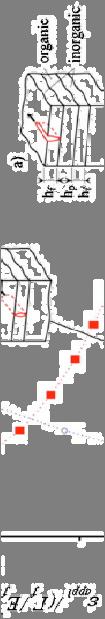


15 Bending Radius = 0 mm Cracking of SiO x N y and Organic/Inorganic Barrier Films on Polymer Substrates σi = E i Z i R Z m optimal Bending Radius = 5 mm safe design space Grego, et al., 2007, Thin Solid Films, Vol. 515, pp ; Cordero, N., Yoon, J., and Suo, Z., 2007, Applied Physics Letters, Vol. 90,
16 Molecular Layer Deposition (MLD) for Multilayer Barrier 2nm ALD Alumina 20 nm SiOxNy Layer 20-nm Polymer 2nm MLD Polymer 3X mechanically improved toughness?x chemically improved toughness due to covalent bonds between polymer and alumina layers 16
17 Contents Atomic Layer Deposition - ALD for micro-scaled devices - ALD for nano-scaled devices - ALD for barrier coating Molecular Layer Deposition - Nylon 66 Progress, Opportunities and Challenges Summary 17

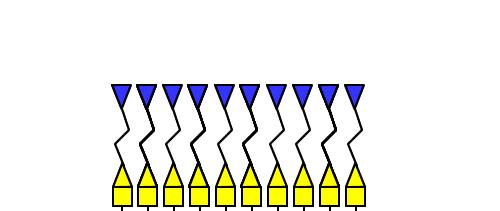
18 Polymer Molecular Layer Deposition (A) (B) 18
19 Precursors for Nylon 66 MLD 16H 1,6-Hexanediamine: i H H N CH 2 CH 2 CH 2 CH 2 CH N H 2 H CH 2 2 Adipoyl Chloride: O Cl CH 2 CH 2 C C CH 2 CH Cl 2 O 19
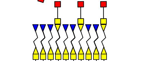
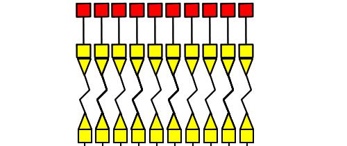
20 Nylon Molecular Layer Deposition 20
21 Nylon Molecular Layer Deposition 21
22 Nylon Molecular Layer Deposition 22
23 Nylon Molecular Layer Deposition 23
24 Nylon Molecular Layer Deposition 24
25 Nylon Molecular Layer Deposition 25
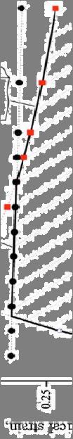
26 Integrated Absorbance Increase versus Number of AB Cycles at 83 C 60 SiO 2 Powder Substrate, 83 o C Integrated Absorbance Start End Combined Absorbance of Amide I and II Bands is Linear with Number of AB Cycles Number of AB Cycles Y. Du & S.M. George, J. Phys. Chem. C 111, 8509 (2007). 26
27 Contents Atomic Layer Deposition - ALD for micro-scaled devices - ALD for nano-scaled devices - ALD for barrier coating Molecular Layer Deposition - Nylon 66 Progress, Opportunities and Challenges Summary 27
28 Atomic Layer Deposition: Progress, Opportunities and Challenges ALD at CU-Boulder (George Research Group) Alumina (Al 2 O 3 ) Tungsten (W) Ruthenium (Ru) Aluminum Nitride (AlN) Tantalum Nitride (TaN) Tin Oxide (SnO 2 ) Silicon Dioxide id (SiO 2 ) Hafnium Oxide (HfO 2 ) Zinc Oxide (ZnO) Titanium Oxide (TiO 2 ) Magnesium Oxide (MgO) Manganese Oxide (MnO 2 ) Hydrophobic Layers ALD processes are well developed. d CVD with binary reactions ALD possible. ALD for MEMS - high quality coatings - manufacturable now - quality (yield/defect)? - reliability? ALD for NEMS - enabling technologies for devices and interfaces - improved processes for novel applications, NT/NW/graphene. 28
29 Atomic and Molecular Layer Deposition: Progress, Opportunities and Challenges Nylon 66 MLD First report by CU in Summer 2006, Others: NC State and Helsinki Institute of Technology Poly(p-Phenylene Ph l Terephthalamide) [PPTA] Kevlar MLD Demonstrated by CU in Spring Higher Thermal Stability Polyamide Polymer Alucone MLD: Novel Hybrid Organic/Inorganic g Polymer. Published by CU and University of Oslo in Summer New Nanocomposite Flexible Polymer. MLD of ABC Polymers. Novel Hybrid Organic/Inorganic Polymer based on ABC Reaction Sequence. Demonstrated by CU in Fall Enlarges Material Set for Nanocomposite Films. ALD/MLD processes are new and good for a large number of inorganic/organic combinations. ALD/MLD for MEMS - > 10X in quality and reliability - new surface properties resulting from polymer layers. ALD/MLD for NEMS - exciting enabling technologies og es for devices and interfaces - organic molecules essential to NEMS; multiple inorganic/organic layers with molecular precision. applications, science and technology? 29


30 Opportunity: ALD/MLD-Enabled Highly Selective, Stable and Manufacturable Biosensors Wei Tan, Xiohua Du, Steven M. George and Y. C. Lee Universal Functionalization Platform Application-Specific p Receptors MLD PEG ALD Alumina ALD Alumina-on-NW NW/NT/MEMS Devices ALD Alumina-on-NT PEG for anti-fouling to reduce false alarms: Single layer PEG coating? density? Multi-layer PEG coating? Conformation? MLD PEG can give us a precise number of high-quality anti-fouling layers for a quantitative understanding leading to highly selective, stable and manufacturable 5 μm biosensors. ALD Alumina-on-MEMS 30
31 Summary Atomic Layer Deposition - ALD for micro-scaled devices - ALD for nano-scaled devices - ALD for barrier coating Molecular Layer Deposition - Nylon 66 Progress, Opportunities and Challenges - ALD for MEMS: manufacturing, quality and reliability - ALD for NEMS: enabling technologies for devices and interfaces for system integration - ALD/MLD for MEMS: >10X improvement over ALD in quality and reliability - ALD/MLD for NEMS: Exciting inorganic/organic multilayers for repeatable, predictable and reliable NEMS. 31
Future Thin and Flexible Systems?
 Packaging and Thermal Management Challenges for Future 1-mm Thin Smartphones? Y. C. Lee, University of Colorado - Boulder Three CU technologies: Flexible thermal ground planes All solid state battery Atomic
Ultrabarriers by Atomic Layer Deposition. Steven M. George Depts. of Chemistry & Chemical Engineering University of Colorado, Boulder, Colorado
 Ultrabarriers by Atomic Layer Deposition Steven M. George Depts. of Chemistry & Chemical Engineering University of Colorado, Boulder, Colorado Outline 1. 2 O 3 ALD barriers on PEN & PET 2. Critical tensile
Microsystem Integration (March 20, 2017)
") Microsystem Integration (March 20, 2017) Mid-term exam: open notes/computers/ - 1:00 to 1:50 p.m., Wednesday, March 22. Homeworks #1 to 7. - Solutions of #1 to 7 are posted. Workshops #1 to 15. - Workshops
Microsystem Integration (March 20, 2017) Mid-term exam: open notes/computers/ - 1:00 to 1:50 p.m., Wednesday, March 22. Homeworks #1 to 7. - Solutions of #1 to 7 are posted. Workshops #1 to 15. - Workshops
Atomic Layer Deposition (ALD)
") Atomic Layer Deposition (ALD) ALD provides Uniform, controlled, conformal deposition of oxide, nitride, and metal thin films on a nanometer scale. ALD is a self limiting thin film deposition technique
Atomic Layer Deposition (ALD) ALD provides Uniform, controlled, conformal deposition of oxide, nitride, and metal thin films on a nanometer scale. ALD is a self limiting thin film deposition technique
Atomic Layer Deposition. ALD process solutions using FlexAL and OpAL
 Atomic Layer Deposition process solutions using FlexAL and OpAL Introduction to Self limiting digital growth Atomic Layer Deposition () offers precisely controlled ultra-thin films for advanced applications
About Cambridge NanoTech Atomic Layer Deposition (ALD) Selected Applications Manufacturing Considerations ALD Reactors Summary
 Selected Applications Manufacturing Considerations ALD Reactors Summary") About Cambridge NanoTech Atomic Layer Deposition (ALD) Selected Applications Manufacturing Considerations ALD Reactors Summary Founded in 2003 by Dr. Jill Becker Located in Cambridge, MA Grew directly
About Cambridge NanoTech Atomic Layer Deposition (ALD) Selected Applications Manufacturing Considerations ALD Reactors Summary Founded in 2003 by Dr. Jill Becker Located in Cambridge, MA Grew directly
ALD and CVD of Copper-Based Metallization for. Microelectronic Fabrication. Department of Chemistry and Chemical Biology
 ALD and CVD of Copper-Based Metallization for Microelectronic Fabrication Yeung Au, Youbo Lin, Hoon Kim, Zhengwen Li, and Roy G. Gordon Department of Chemistry and Chemical Biology Harvard University Introduction
WŝŽŶĞĞƌŝŶŐ > ĞdžƉĞƌŝĞŶĐĞ ƐŝŶĐĞ ϭϵϳϰ WŝĐŽƐƵŶ ^he > Ρ WͲƐĞƌŝĞƐ > ƐLJƐƚĞŵƐ ƌŝěőŝŷő ƚśğ ŐĂƉ ďğƚǁğğŷ ƌğɛğăƌđś ĂŶĚ ƉƌŽĚƵĐƟŽŶ d, &hdhz K& d,/e &/>D /^, Z
 The ALD Powerhouse Picosun Defining the future of ALD Picosun s history and background date back to the very beginning of the field of atomic layer deposition. ALD was invented in Finland in 1974 by Dr.
Properties of atomic layer deposited Al 2 O 3 /ZnO dielectric films grown at low temperature for RF MEMS
 Properties of atomic layer deposited Al O /ZnO dielectric films grown at low temperature for RF MEMS Cari F. Herrmann *a,b, Frank W. DelRio a, Steven M. George b,c, Victor M. Bright a a Department of Mechanical
High Barrier Multi-Layer Parylene Coating
 High Barrier Multi-Layer Parylene Coating Technology overview Surface Technolgy 2018 Company Profile Swiss company founded in 1979 Experts in Parylene coating technology Parylene Equipment Export rate
Supporting Information
 Supporting Information Vapor-Phase Atomic-Controllable Growth of Amorphous Li 2 S for High-Performance Lithium-Sulfur Batteries Xiangbo Meng, David J. Comstock, Timothy T. Fister, and Jeffrey W. Elam *
Activities in Plasma Process Technology at SENTECH Instruments GmbH, Berlin. Dr. Frank Schmidt
 Activities in Plasma Process Technology at SENTECH Instruments GmbH, Berlin Dr. Frank Schmidt The Company Company Private company, founded 1990 80 employees ISO 9001 Location Science & Technology Park,
Encapsulation of Indium-Gallium-Zinc Oxide Thin Film Transistors
 Encapsulation of Indium-Gallium-Zinc Oxide Thin Film Transistors Encapsulation Layer Al gate Source IGZO Gate Drain Si JULIA OKVATH HIRSCHMAN RESEARCH GROUP @ RIT MAY 9, 2017 Outline Brief Introduction
Low temperature deposition of thin passivation layers by plasma ALD
 1 Low temperature deposition of thin passivation layers by plasma ALD Bernd Gruska, SENTECH Instruments GmbH, Germany 1. SENTECH in brief 2. Low temperature deposition processes 3. SENTECH SI ALD LL System
Manipulation and control of spatial ALD layers for flexible devices. Aimcal Memphis 2016; Edward Clerkx
 Manipulation and control of spatial ALD layers for flexible devices Meyer Burger Netherlands Equipment manufacturer Functional inkjet printing Based in Eindhoven, the Netherlands Part of world-wide Meyer
Extending product lifetime with ALD moisture barrier
 Whitepaper Extending product lifetime with ALD moisture barrier 01 executive summary Atomic Layer Deposition (ALD) is a thin film technology that enables new and highly competitive products. Typical applications
ALD Atomic Layer Deposition
 ALD Atomic Layer Deposition Christophe Vallée Laboratoire des Technologies de la Microélectronique (LTM) Univ. Grenoble Alpes, Lab. LTM (CEA-LETI/MINATEC) - Grenoble France christophe.vallee@cea.fr 1.
Atomic Oxygen-Resistant, Static-Dissipative, Pinhole-Free Coatings for Spacecraft
 Physical Sciences Inc. VG10-109 Atomic Oxygen-Resistant, Static-Dissipative, Pinhole-Free Coatings for Spacecraft Michelle T. Schulberg, Robert H. Krech, Frederick S. Lauten Physical Sciences Inc. Roy
National Nano Fabrication Centre (NNFC)
") National Nano Fabrication Centre (NNFC) Tool and Process Capabilities 1. Lithography 1.1 Direct Laser Writer/Lithography 1.1.1 Preferred Design file format: GDS2 or CIF 1.1.2 Please note that coloured
National Nano Fabrication Centre (NNFC) Tool and Process Capabilities 1. Lithography 1.1 Direct Laser Writer/Lithography 1.1.1 Preferred Design file format: GDS2 or CIF 1.1.2 Please note that coloured
ALD systems and SENTECH Instruments GmbH
 ALD systems and processes @ SENTECH Instruments GmbH H. Gargouri, F. Naumann, R. Rudolph and M. Arens SENTECH Instruments GmbH, Berlin www.sentech.de 1 2 Agenda 1. Company Introduction 2. SENTECH-ALD-Systems
ALD of Copper and Copper Oxide Thin Films for Applications in Metallization Systems of ULSI Devices
 ALD of Copper and Copper Oxide Thin Films for Applications in Metallization Systems of ULSI Devices a, Steffen Oswald b, Nina Roth c, Heinrich Lang c, Stefan E. Schulz a,d, and Thomas Gessner a,d a Center
11:30 AM - C4.4 Chemical Vapor Deposition of Cobalt Nitride and Its Application as an Adhesion-enhancing Layer for Advanced Copper Interconnects
 2012-04-11 SYMPOSIUM C 11:30 AM - C4.4 Chemical Vapor Deposition of Cobalt Nitride and Its Application as an Adhesion-enhancing Layer for Advanced Copper Interconnects Jing Yang 1, Harish B. Bhandari 1,
Oxide Growth. 1. Introduction
 Oxide Growth 1. Introduction Development of high-quality silicon dioxide (SiO2) has helped to establish the dominance of silicon in the production of commercial integrated circuits. Among all the various
In-situ Monitoring of Atomic Layer Deposition Processes
 Faculty of Electrical and Computer Engineering - Institute of Semiconductors and Microsystems NanoZEIT seminar @ SEMICON 2011 Deposition Processes M. Knaut*, M. Junige, M. Geidel, M. Albert, and J. W.
Atomic Layer Deposition
 Atomic Layer Deposition Ville Malinen R&D Engineer Nanopinnoitteita koneenrakentajille 2010 1 Introduction 1) Overview of Beneq 2) Atomic Layer Deposition (ALD), to deposit thin films, which Are dense
Growth of Y 2 O 3 and HfO 2 as Single Compounds and as Nanolaminates on Si using Atomic Layer Deposition Adam Kueltzo
 Growth of Y 2 O 3 and HfO 2 as Single Compounds and as Nanolaminates on Si using Atomic Layer Deposition Adam Kueltzo Thornton Fractional North High School July 31 st, 2008 University of Illinois at Chicago
Materials and Processing Issues Associated With Seal Coating Development
 Materials and Processing Issues Associated With Seal Coating Development J. D. Meyer and W. Y. Lee Department of Chemical, Biochemical, and Materials Engineering Stevens Institute of Technology 23 rd Annual
Precursors with Metal-Nitrogen Bonds for ALD of Metals, Nitrides and Oxides
 Precursors with Metal-Nitrogen Bonds for ALD of Metals, Nitrides and Oxides Abstract Roy Gordon Gordon@chemistry.harvard.edu, Cambridge, MA To achieve ALD s unique characteristics, ALD precursors must
Material Evaporation Application Comment MP P / Optical films, Oxide films, Electrical contacts. Doping, Electrical contacts.
 for vapour Aluminum (Al) -, Optical, Oxide, Electrical BN liners with lid are recommended due to the reactivity and the fact that Al creeps out. Cooling down of the cell with 1K per minute. 660 972 Antimony
Roll-to-Roll ALD Deposition of Al 2 O 3 Barrier Layers on PET
 Roll-to-Roll ALD Deposition of Al 2 O 3 Barrier Layers on PET W. A. Barrow and E. R. Dickey Lotus Applied Technology AIMCAL Fall Technical Conference 2009 Amelia Island Plantation, Florida 20-Oct-2009
New Surface Properties by Atomic Layer Deposition
 New Surface Properties by Atomic Layer Deposition Beneq Oy, Finland Dr Tommi Vainio, CTO HANNOVER MESSE MicroTechnology Forum Innovations for Industry April 21, 2009 Turning Innovations into Success 1
Chapter 3 Silicon Device Fabrication Technology
 Chapter 3 Silicon Device Fabrication Technology Over 10 15 transistors (or 100,000 for every person in the world) are manufactured every year. VLSI (Very Large Scale Integration) ULSI (Ultra Large Scale
1 MARCH 2017 FILM DEPOSITION NANOTECHNOLOGY
 1 MARCH 2017 FILM DEPOSITION NANOTECHNOLOGY PRESENTATION Pedro C. Feijoo E-mail: PedroCarlos.Feijoo@uab.cat FABRICATION TECHNOLOGIES FOR NANOELECTRONIC DEVICES. PEDRO C. FEIJOO 2 FILM GROWTH Chemical vapor
Fiji Thermal and Plasma Atomic Layer Deposition System (ALD) By Ultratech (Cambridge)
 By Ultratech (Cambridge)") Fiji Thermal and Plasma Atomic Layer Deposition System (ALD) By Ultratech (Cambridge) PREPARED BY: You-Sheng (Wilson) Lin, Nanolab Staff 7-30-2013 Superusers: Steve Franz You-Sheng Lin Max Ho X68923 X68923
Fiji Thermal and Plasma Atomic Layer Deposition System (ALD) By Ultratech (Cambridge) PREPARED BY: You-Sheng (Wilson) Lin, Nanolab Staff 7-30-2013 Superusers: Steve Franz You-Sheng Lin Max Ho X68923 X68923
EECS130 Integrated Circuit Devices
 EECS130 Integrated Circuit Devices Professor Ali Javey 9/13/2007 Fabrication Technology Lecture 1 Silicon Device Fabrication Technology Over 10 15 transistors (or 100,000 for every person in the world)
Enhanced moisture-barrier property and flexibility of zirconium oxide/polymer hybrid structures
 Korean J. Chem. Eng., 33(3), 1070-1074 (2016) DOI: 10.1007/s11814-015-0225-5 INVITED REVIEW PAPER pissn: 0256-1115 eissn: 1975-7220 Enhanced moisture-barrier property and flexibility of zirconium oxide/polymer
Morphology and High-temperature Stability of Amorphous Alumina Coatings Deposited on Si and CeO 2 -Stabilized ZrO 2 by MOCVD
 Morphology and High-temperature Stability of Amorphous Alumina Coatings Deposited on Si and CeO 2 -Stabilized ZrO 2 by MOCVD J. D. Meyer and W. Y. Lee Dept. of Materials Science & Engineering Stevens Institute
Atomic Layer Deposition An Introduction to Theory and Applications
 Atomic Layer Deposition An Introduction to Theory and Applications Eric Deguns Ph.D. October 4, 2011 Agenda Atomic Layer Deposition Overview History Applications Summary Cambridge NanoTech Methods for
Change in stoichiometry
 Measurement of Gas Sensor Performance Gas sensing materials: 1. Sputtered ZnO film (150 nm (Massachusetts Institute of Technology) 2. Sputtered SnO 2 film (60 nm) (Fraunhofer Institute of Physical Measurement
Lecture 19 Microfabrication 4/1/03 Prof. Andy Neureuther
 EECS 40 Spring 2003 Lecture 19 Microfabrication 4/1/03 Prof. ndy Neureuther How are Integrated Circuits made? Silicon wafers Oxide formation by growth or deposition Other films Pattern transfer by lithography
X-Ray Reflectivity Study of Hafnium Silicate Thin Films Prepared by Thermal Chemical Vapor Deposition
 X-Ray Reflectivity Study of Hafnium Silicate Thin Films Prepared by Thermal Chemical Vapor Deposition Hideyuki YAMAZAKI, Advanced LSI Technology Laboratory, Toshiba Corporation hideyuki.yamazaki@toshiba.co.jp
Enhanced Thermal Conductivity of Polyimide Films via a Hybrid of Micro- and Nano-Sized Boron Nitride
 The 2012 World Congress on Advances in Civil, Environmental, and Materials Research (ACEM 12) Seoul, Korea, August 26-30, 2012 Enhanced Thermal Conductivity of Polyimide Films via a Hybrid of Micro- and
EE 330 Lecture 8. IC Fabrication Technology Part II. - Oxidation - Epitaxy - Polysilicon - Interconnects
 EE 330 Lecture 8 IC Fabrication Technology Part II - Oxidation - Epitaxy - Polysilicon - Interconnects Review from Last Time MOS Transistor Bulk Source Gate Drain p-channel MOSFET Lightly-doped n-type
A New Liquid Precursor for Pure Ruthenium Depositions. J. Gatineau, C. Dussarrat
 1.1149/1.2727414, The Electrochemical Society A New Liquid Precursor for Pure Ruthenium Depositions J. Gatineau, C. Dussarrat Air Liquide Laboratories, Wadai 28, Tsukuba city, Ibaraki Prefecture, 3-4247,
Lecture Day 2 Deposition
 Deposition Lecture Day 2 Deposition PVD - Physical Vapor Deposition E-beam Evaporation Thermal Evaporation (wire feed vs boat) Sputtering CVD - Chemical Vapor Deposition PECVD LPCVD MVD ALD MBE Plating
Visit
 Practical Applications for Nano- Electronics by Vimal Gopee E-mail: Vimal.gopee@npl.co.uk 10/10/12 Your Delegate Webinar Control Panel Open and close your panel Full screen view Raise hand for Q&A at the
Microfabrication of Integrated Circuits
 Microfabrication of Integrated Circuits OUTLINE History Basic Processes Implant; Oxidation; Photolithography; Masks Layout and Process Flow Device Cross Section Evolution Lecture 38, 12/05/05 Reading This
[Supporting Information] Piezopotential Gated Nanowire-Nanotube-Hybrid Field-Effect- Transistor
![[Supporting Information] Piezopotential Gated Nanowire-Nanotube-Hybrid Field-Effect- Transistor](/thumbs/86/93491906.jpg "[Supporting Information] Piezopotential Gated Nanowire-Nanotube-Hybrid Field-Effect- Transistor") [Supporting Information] Piezopotential Gated Nanowire-Nanotube-Hybrid Field-Effect- Transistor Weihua Liu 1,3, Minbaek Lee 1, Lei Ding 2, Jie Liu 2, Zhong Lin Wang 1* Authors equally contributed. 1 School
[Supporting Information] Piezopotential Gated Nanowire-Nanotube-Hybrid Field-Effect- Transistor Weihua Liu 1,3, Minbaek Lee 1, Lei Ding 2, Jie Liu 2, Zhong Lin Wang 1* Authors equally contributed. 1 School
Silicon Epitaxial CVD Want to create very sharp PN boundary grow one type layer on other in single crystal form High dopant layers on low dopant
 Silicon Epitaxial CVD Want to create very sharp PN boundary grow one type layer on other in single crystal form High dopant layers on low dopant substrate Creates latch up protection for CMOS Buried Epi
2. Fabrication techniques. KNU Seminar Course 2015 Robert Mroczyński
 2. Fabrication techniques KNU Seminar Course 2015 Robert Mroczyński Technological layers used in the course of the IC fabrication Semiconductors Fundamental part of each IC, active material of semiconductor
Flexible functional devices at mass production level with the FLEx R2R sald platform
 Flexible functional devices at mass production level with the FLEx R2R sald platform D. Spee, W. Boonen, D. Borsa and E. Clerkx Meyer Burger (Netherlands) B.V. Meyer Burger Introduction to sald Challenges
Complexity of IC Metallization. Early 21 st Century IC Technology
 EECS 42 Introduction to Digital Electronics Lecture # 25 Microfabrication Handout of This Lecture. Today: how are Integrated Circuits made? Silicon wafers Oxide formation by growth or deposition Other
Processing of Semiconducting Materials Prof. Pallab Banerjee Department of Material Science Indian Institute of Technology, Kharagpur
 Processing of Semiconducting Materials Prof. Pallab Banerjee Department of Material Science Indian Institute of Technology, Kharagpur Lecture - 35 Oxidation I (Refer Slide Time: 00:24) Today s topic of
Instructor: Dr. M. Razaghi. Silicon Oxidation
 SILICON OXIDATION Silicon Oxidation Many different kinds of thin films are used to fabricate discrete devices and integrated circuits. Including: Thermal oxides Dielectric layers Polycrystalline silicon
IMRE/ETPL Flagship Project
 IMRE/ETPL Flagship Project Nanoparticulate Barrier Films & Gas Permeation Measurement Techniques for Thin Film Solar & Display Application Problems Senthil Ramadas Institute of Materials Research & Engineering
Application of ultra-thin aluminum oxide etch mask made by atomic layer deposition technique
 IOP Publishing Journal of Physics: Conference Series 61 (2007) 369 373 doi:10.1088/1742-6596/61/1/074 International Conference on Nanoscience and Technology (ICN&T 2006) Application of ultra-thin aluminum
KGC SCIENTIFIC Making of a Chip
 KGC SCIENTIFIC www.kgcscientific.com Making of a Chip FROM THE SAND TO THE PACKAGE, A DIAGRAM TO UNDERSTAND HOW CPU IS MADE? Sand CPU CHAIN ANALYSIS OF SEMICONDUCTOR Material for manufacturing process
Nanoscale Barrier Coating on BOPP Packaging Film by ALD Presented by: Dr. Johanna Lahti Senior Research Fellow Tampere University of Technology
 Nanoscale Barrier Coating on BPP Packaging Film by ALD Presented by: Dr. Johanna Lahti Senior Research Fellow Tampere University of Technology Co-authors: Kimmo Lahtinen (LUT*), Petri Johansson (TUT),
Lecture 7 Metal Oxide Semiconductors
 Lecture 7 Metal Oxide Semiconductors 1/73 Announcements Homework 1/4: I will return it next Tuesday (October 16 th ). Homework 2/4: Will be online on later today. Due Thursday October 18 th at the start
Simple fabrication of highly ordered AAO nanotubes
 Journal of Optoelectronic and Biomedical Materials Volume 1, Issue 1, March 2009, p. 79-84 Simple fabrication of highly ordered AAO nanotubes N. Taşaltin a, S. Öztürk a, H. Yüzer b, Z. Z. Öztürk a,b* a
Lecture 4. Oxidation (applies to Si and SiC only) Reading: Chapter 4
 Reading: Chapter 4") Lecture 4 Oxidation (applies to Si and SiC only) Reading: Chapter 4 Introduction discussion: Oxidation: Si (and SiC) Only The ability to grow a high quality thermal oxide has propelled Si into the forefront
Lecture 4 Oxidation (applies to Si and SiC only) Reading: Chapter 4 Introduction discussion: Oxidation: Si (and SiC) Only The ability to grow a high quality thermal oxide has propelled Si into the forefront
Thermal Evaporation. Theory
 Thermal Evaporation Theory 1. Introduction Procedures for depositing films are a very important set of processes since all of the layers above the surface of the wafer must be deposited. We can classify
Mox/CNTs hetero-structures for gas sensing applications: Role of CNTs defects
 Iowa State University From the SelectedWorks of Jean-Philippe Tessonnier 2012 Mox/CNTs hetero-structures for gas sensing applications: Role of CNTs defects G. Neri, University of Messina S. G. Leonardi,
Effect of annealing temperature on the electrical properties of HfAlO thin films. Chun Lia, Zhiwei Heb*
 International Forum on Energy, Environment and Sustainable Development (IFEESD 2016) Effect of annealing temperature on the electrical properties of HfAlO thin films Chun Lia, Zhiwei Heb* Department of
Tribological and Catalytic Coatings
 Tribological and Catalytic Coatings Objectives: Study of mechanical properties of nanocomposite and nanolaminate thin films deposited by pulsed laser deposition (PLD): Nitride-based coatings (AlN, TiN,
Progress in Roll-to-Roll Atomic Layer Deposition
 Progress in Roll-to-Roll Atomic Layer Deposition Council for Chemical Research Barrier Workshop Arlington, Virginia September 20, 2012 E. Dickey Lotus Applied Technology Outline ALD for barrier films ALD
Engineering Materials
 Engineering Materials Lecture 2 MEL120: Manufacturing Practices 1 Selection of Material A particular material is selected is on the basis of following considerations 1. Properties of material 1. Properties
NCERCAMP at the University of Akron. Major Equipment
 Tescan LYRA-3 Model XMU FIB-FESEM Scanning Electron Microscope (SEM) with Focused Ion Beam (FIB) capability and a Transmission Electron Microscope (STEM) detector. The FIB can perform cross sectioning
TED PELLA, INC. Microscopy Products for Science and Industry
 PELCO SILICON NITRIDE, SILICON DIOXIDE, BLANK SILICON SUBSTRATES & APERTURES FOR TEM Clean, Debris-free with Exact 3mm TEM Frame and EasyGrip Edges PELCO Silicon Nitride Support Films for TEM Hydrophilic
Supplementary Figure 1 In situ QCM measurements of Pd ALD on different oxide
 Supplementary Figure 1 In situ QCM measurements of Pd ALD on different oxide surfaces using either HCHO or H 2 as reducing agent at 150 ºC. (a) On Al 2 O 3 ; (b) on ZrO 2 ; (c), on TiO 2. See Supplementary
Review Literature for Mosfet Devices Using High- K
 Review Literature for Mosfet Devices Using High- K Prerna Teaching Associate, Deptt of E.C.E., G.J.U.S. &T., INDIA prernaa.29@gmail.com Abstract: With the advancement of MOS devices over 40 years ago,
Alternative Methods of Yttria Deposition For Semiconductor Applications. Rajan Bamola Paul Robinson
 Alternative Methods of Yttria Deposition For Semiconductor Applications Rajan Bamola Paul Robinson Origin of Productivity Losses in Etch Process Aggressive corrosive/erosive plasma used for etch Corrosion/erosion
Atomic Layer Deposition
 Atomic Layer Deposition FlexAL and OpAL TM The Business of Science Introduction to ALD Self limiting digital growth Atomic Layer Deposition (ALD) offers the opportunity to create precisely controlled ultra-thin
Barix Multilayers: a Water and Oxygen Barrier for Flexible Organic Electronics. Robert Jan Visser
 Barix Multilayers: a Water and Oxygen Barrier for Flexible Organic Electronics Robert Jan Visser Organic Electronics Is the Future of Electronics Organic? MIT Stanford UC Berkeley Nano Forum Vitex Systems,
Thin Films: Sputtering Systems (Jaeger Ch 6 & Ruska Ch 7,) Can deposit any material on any substrate (in principal) Start with pumping down to high
 Can deposit any material on any substrate (in principal) Start with pumping down to high") Thin Films: Sputtering Systems (Jaeger Ch 6 & Ruska Ch 7,) Can deposit any material on any substrate (in principal) Start with pumping down to high vacuum ~10-7 torr Removes residual gases eg oxygen from
Thin Films: Sputtering Systems (Jaeger Ch 6 & Ruska Ch 7,) Can deposit any material on any substrate (in principal) Start with pumping down to high vacuum ~10-7 torr Removes residual gases eg oxygen from
Surface Preparation and Cleaning Conference April 19-20, 2016, Santa Clara, CA, USA. Nano-Bio Electronic Materials and Processing Lab.
 Surface Preparation and Cleaning Conference April 19-20, 2016, Santa Clara, CA, USA Issues on contaminants on EUV mask Particle removal on EUV mask surface Carbon contamination removal on EUV mask surface
Conductive Gas Barriers Prepared by Using Atomic Layer Deposition Technique
 Available online at www.sciencedirect.com Procedia Engineering 36 (2012 ) 562 570 IUMRS-ICA 2011 Conductive Gas Barriers Prepared by Using Atomic Layer Deposition Technique Chih-Chieh Yu*, Meng-Yen Tsai,
MICROCHIP MANUFACTURING by S. Wolf
 MICROCHIP MANUFACTURING by S. Wolf Chapter 7: BASICS OF THIN FILMS 2004 by LATTICE PRESS Chapter 7: Basics of Thin Films CHAPTER CONTENTS Terminology of Thin Films Methods of Thin-Film Formation Stages
Examples of dry etching and plasma deposition at Glasgow University
 Examples of dry etching and plasma deposition at Glasgow University Glasgow has pioneered and established many novel research activities involving the development of new dry etch processes and dry etch
Atomic Layer Deposition of Novel High Dielectric Constant Materials
 Atomic Layer Deposition of Novel High Dielectric Constant Materials Adam Kueltzo # & Julie Lam * Thornton Fractional North High School # and Maine East High School * August 2, 2007 University of Illinois
High Transmittance Ti doped ITO Transparent Conducting Layer Applying to UV-LED. Y. H. Lin and C. Y. Liu
 High Transmittance Ti doped ITO Transparent Conducting Layer Applying to UV-LED Y. H. Lin and C. Y. Liu Department of Chemical Engineering and Materials Engineering, National Central University, Jhongli,
Lecture 8. Deposition of dielectrics and metal gate stacks (CVD, ALD)
") Lecture 8 Deposition of dielectrics and metal gate stacks (CVD, ALD) Thin Film Deposition Requirements Many films, made of many different materials are deposited during a standard CMS process. Gate Electrodes
Lecture 8 Deposition of dielectrics and metal gate stacks (CVD, ALD) Thin Film Deposition Requirements Many films, made of many different materials are deposited during a standard CMS process. Gate Electrodes
EE 5611 Introduction to Microelectronic Technologies Fall Tuesday, September 04, 2012 Lecture 01
 EE 5611 Introduction to Microelectronic Technologies Fall 2012 Tuesday, September 04, 2012 Lecture 01 1 Instructor: Jing Bai Contact Email: jingbai@d.umn.edu, hone: (218)726-8606, Office: MWAH 255 Webpage:
Silicon Epitaxial CVD Want to create very sharp PN boundary grow one type layer on other in single crystal form High dopant layers on low dopant
 Silicon Epitaxial CVD Want to create very sharp PN boundary grow one type layer on other in single crystal form High dopant layers on low dopant substrate Creates latch up protection for CMOS Buried Epi
Semiconductor Manufacturing Technology. Semiconductor Manufacturing Technology
 Semiconductor Manufacturing Technology Michael Quirk & Julian Serda October 2001 by Prentice Hall Chapter 10 Oxidation 2001 2000 by Prentice Hall Diffusion Area of Wafer Fabrication Wafer fabrication (front-end)
Micro-Electro-Mechanical Systems (MEMS) Fabrication. Special Process Modules for MEMS. Principle of Sensing and Actuation
 Fabrication. Special Process Modules for MEMS. Principle of Sensing and Actuation") Micro-Electro-Mechanical Systems (MEMS) Fabrication Fabrication Considerations Stress-Strain, Thin-film Stress, Stiction Special Process Modules for MEMS Bonding, Cavity Sealing, Deep RIE, Spatial forming
Micro-Electro-Mechanical Systems (MEMS) Fabrication Fabrication Considerations Stress-Strain, Thin-film Stress, Stiction Special Process Modules for MEMS Bonding, Cavity Sealing, Deep RIE, Spatial forming
ANTI-STICTION COATINGS FOR HIGH RELIABILITY MEMS
 ANTI-STICTION COATINGS FOR HIGH RELIABILITY MEMS Introduction Nilesh Gunda, Santosh K. Jha and Suri A. Sastri Surmet Corporation, 33 B Street Burlington, MA 01803 (USA). Micro-electromechanical system
Continuous and R2R ALD for Coating of Polymer Webs
 Continuous and R2R ALD for Coating of Polymer Webs AIMCAL 2011 Web Coating Conference Dr. Mikko Söderlund Application Manager Cost of ownership [ /m 2 ] R2R ALD a paradigm change Large-area (batch) ALD
Silicon Microfabrication Part 2
 Introduction to BioMEMS & Medical Microdevices Silicon Microfabrication Part 2 Companion lecture to the textbook: Fundamentals of BioMEMS and Medical Microdevices, by Prof., http://saliterman.umn.edu/
Overview. Silicon Microfabrication Part 2. Introduction to BioMEMS & Medical Microdevices
 Introduction to BioMEMS & Medical Microdevices Silicon Microfabrication Part 2 Companion lecture to the textbook: Fundamentals of BioMEMS and Medical Microdevices, by Prof., http://saliterman.umn.edu/
Mostafa Soliman, Ph.D. May 5 th 2014
 Mostafa Soliman, Ph.D. May 5 th 2014 Mostafa Soliman, Ph.D. 1 Basic MEMS Processes Front-End Processes Back-End Processes 2 Mostafa Soliman, Ph.D. Wafers Deposition Lithography Etch Chips 1- Si Substrate
Photovoltaics & Solar Thermals. Thin-film equipment. Customized. FHR Anlagenbau GmbH I
 Photovoltaics & Solar Thermals Thin-film equipment. Customized. FHR Anlagenbau GmbH I www.fhr.de FHR Anlagenbau GmbH is an innovative enterprise in the branch of vacuum processing and thin-film technologies.
Chemical Vapour Deposition: CVD Reference: Jaeger Chapter 6 & Ruska: Chapter 8 CVD - Chemical Vapour Deposition React chemicals to create a thin film
 Chemical Vapour Deposition: CVD Reference: Jaeger Chapter 6 & Ruska: Chapter 8 CVD - Chemical Vapour Deposition React chemicals to create a thin film layer at the surface Typically gas phase reactions
CMOS Technology. Flow varies with process types & company. Start with substrate selection. N-Well CMOS Twin-Well CMOS STI
 CMOS Technology Flow varies with process types & company N-Well CMOS Twin-Well CMOS STI Start with substrate selection Type: n or p Doping level, resistivity Orientation, 100, or 101, etc Other parameters
EE 330 Lecture 9. IC Fabrication Technology Part 2
 EE 330 Lecture 9 IC Fabrication Technology Part 2 Quiz 8 A 2m silicon crystal is cut into wafers using a wire saw. If the wire diameter is 220um and the wafer thickness is 350um, how many wafers will this
Dielectric II-VI and IV-VI Metal Chalcogenide Thin Films in Hollow Glass Waveguides (HGWs) for Infrared Spectroscopy and Laser Delivery
 for Infrared Spectroscopy and Laser Delivery") Dielectric II-VI and IV-VI Metal Chalcogenide Thin Films in Hollow Glass Waveguides (HGWs) for Infrared Spectroscopy and Laser Delivery Carlos M. Bledt * a, Daniel V. Kopp a, and James A. Harrington a
Dielectric II-VI and IV-VI Metal Chalcogenide Thin Films in Hollow Glass Waveguides (HGWs) for Infrared Spectroscopy and Laser Delivery Carlos M. Bledt * a, Daniel V. Kopp a, and James A. Harrington a
ENCAPSULATION BARRIER LAYERS
 ENCAPSULATION BARRIER LAYERS PUBLICATION REVIEW ON SAVANNAH & FIJI 07.20.2015 1 Humidity Barriers * WVTR: Water Vapor Transmission Rate [g/m 2 /day] Food packaging Advanced Barriers TradiPonal Barriers
ATOMIC LAYER DEPOSITION OF 2D TRANSITION METAL DICHALOGENIDES
 ATOMIC LAYER DEPOSITION OF 2D TRANSITION METAL DICHALOGENIDES Annelies Delabie, M. Caymax, B. Groven, M. Heyne, K. Haesevoets, J. Meersschaut, T. Nuytten, H. Bender, T. Conard, P. Verdonck, S. Van Elshocht,
Area-selective atomic layer deposition for self-aligned fabrication
 Area-selective atomic layer deposition for self-aligned fabrication Adrie Mackus Eindhoven University a.j.m.mackus@tue.nl Area-selective ALD for bottom-up processing Top-down Bottom-up Building technology
STUDY OF INFLUENCE OF IN SITU CLEANING PROCESS ON THE QUALITY OF PECVD SiO 2 / LPCVD POLYSILICON INTERFACE
 STUDY OF INFLUENCE OF IN SITU CLEANING PROCESS ON THE QUALITY OF PECVD SiO 2 / LPCVD POLYSILICON INTERFACE Abstract ANA NEILDE R. DA SILVA, NILTON MORIMOTO, OLIVIER BONNAUD* neilde@lsi.usp.br - morimoto@lsi.usp.br