Portland Technology Development, * CR, # QRE, % PTM Intel Corporation
|
|
|
- Elizabeth Cannon
- 6 years ago
- Views:
Transcription
1 A 45nm Logic Technology with High-k + Metal Gate Transistors, Strained Silicon, 9 Cu Interconnect Layers, 193nm Dry Patterning, and 100% Pb-free Packaging K. Mistry, C. Allen, C. Auth, B. Beattie, D. Bergstrom, M. Bost, M. Brazier, M. Buehler, A. Cappellani, R. Chau *, C.-H. Choi, G. Ding, K. Fischer, T. Ghani, R. Grover, W. Han, D. Hanken, M. Hattendorf, J. He #, J. Hicks #, R. Heussner, D. Ingerly, P. Jain, R. James, L. Jong, S. Joshi, C. Kenyon, K. Kuhn, K. Lee, H. Liu, J. Maiz #, B. McIntyre, P. Moon, J. Neirynck, S. Pae #, C. Parker, D. Parsons, C. Prasad #, L. Pipes, M. Prince, P. Ranade, T. Reynolds, J. Sandford, L. Shifren %, J. Sebastian, J. Seiple, D. Simon, S. Sivakumar, P. Smith, C. Thomas, T. Troeger, P. Vandervoorn, S. Williams, K. Zawadzki Portland Technology Development, * CR, # QRE, % PTM Intel Corporation
2 Outline Introduction Process Features Transistors Interconnects Manufacturing Conclusions 2
 Tox (nm) SiON Silicon 100 10 1 0.1 Gate Leakage (Rel.) 1 0.")
3 Introduction SiON scaling running out of atoms Poly depletion limits inversion T OX scaling 10 Poly 1000 Electrical (Inv) Tox (nm) SiON Silicon Gate Leakage (Rel.) nm 250nm 180nm 130nm 90nm 65nm 3
4 High-k + Metal Gate Benefits High-k gate dielectric Reduced gate leakage T OX scaling Metal gates Eliminate polysilicon depletion Resolves V T pinning and poor mobility for high-k dielectrics 4
5 High-k + Metal Gate Challenges High-k gate dielectric Poor mobility, V T pinning due to soft optical phonons Poor reliability Metal gates Dual bandedge workfunctions Thermal stability Integration scheme 5
6 Outline Introduction Process Features Transistors Interconnects Manufacturing Conclusions 6
7 Process Features 45 nm Groundrules 193 nm Dry Lithography High-K + Metal Gate Transistors 3 RD Generation Strained Silicon Trench Contacts with Local Routing 9 Cu Interconnect Layers 100% Lead-free Packaging 7
8 Process Features 45 nm Groundrules 193 nm Dry Lithography High-K + Metal Gate Transistors 3 RD Generation Strained Silicon Trench Contacts with Local Routing 9 Cu Interconnect Layers 100% Lead-free Packaging 8
9 45nm Design Rules Layer Pitch (nm) Thick (nm) Aspect Ratio Isolation Contacted Gate Metal Metal Metal Metal Metal Metal Metal Metal Metal μm 7μm 0.4 ~0.7x linear scaling from 65nm 9
10 Contacted Gate Pitch Transistor gate pitch of 160 nm continues 0.7x per generation scaling Contacted Gate Pitch (nm) Pitch 250nm 180nm 130nm 90nm 65nm 45nm Technology Node 0.7x every 2 years Tightest contacted gate pitch reported for 45 nm generation
 1 0.5x every 2 years 0.")
11 SRAM Cells μm 2 and μm 2 SRAM cells Optimize density and power/performance 10 SRAM Cell Size ( μm 2 ) 1 0.5x every 2 years nm 180nm 130nm 90nm 65nm 45nm Technology Node Transistor density doubles every two years 11
12 SRAM Array Density SRAM array density achieves 1.9 Mb/mm 2 Includes row/column drivers and other circuitry SRAM Array Density (Mb/mm 2 ) Mb/mm nm 65nm 45nm Array density scales at ~2X per generation 12
13 Outline Introduction Process Features Transistors Interconnects Manufacturing Conclusions 13
14 Transistor Process Flow Key considerations Integrate hafnium-based high-k dielectric, dual metal gate electrodes, strained silicon Thermal stability of metal gate electrodes High-k First, Metal Gate Last Metal gate deposition after high temperature anneals Integrated with strained silicon process Transistor mask count same as 65nm 14
15 Transistor Process Flow Dummy Polysilicon n-ext n-ext p-ext p-ext STI High-k High-k p-well N-well Standard process except for ALD high-k 15a
16 Transistor Process Flow ILD0 N+ N+ STI SiGe SiGe p-well N-well e-sige & S/D, Thermal anneal, ILD0 deposition 15b
17 Transistor Process Flow N+ N+ STI SiGe SiGe p-well N-well Poly Opening Polish 15c
18 Transistor Process Flow N+ N+ STI SiGe SiGe p-well N-well Dummy Poly removal 15d
19 Transistor Process Flow N+ N+ STI SiGe SiGe p-well N-well PMOS WF Metal deposition 15e
20 Transistor Process Flow N+ N+ STI SiGe SiGe p-well N-well PMOS WF Metal patterning 15f
21 Transistor Process Flow N+ N+ STI SiGe SiGe p-well N-well NMOS WF Metal deposition 15g
22 Transistor Process Flow Al fill N+ N+ STI SiGe SiGe p-well N-well Metal Gate trenches filled with low resistance Al 15h
23 Transistor Process Flow N+ N+ STI SiGe SiGe p-well N-well Metal Gate Polish 15i
24 Transistor Process Flow Low Resistance Al Fill NMOS WF PMOS WF N+ N+ STI SiGe SiGe High-k High-k p-well N-well High-k + Metal gate transistor formation complete 15j
25 Transistor Features 35 nm min. gate length 160 nm contacted gate pitch 1.0 nm EOT Hi-K Dual workfunction metal gate electrodes 3 RD generation of strained silicon 16
26 Gate Leakage Gate leakage is reduced >25X for NMOS and 1000X for PMOS Normalized Gate Leakage SiON/Poly 65nm SiON/Poly 65nm HiK+MG 45nm HiK+MG 45nm PMOS NMOS nm: Bai, 2004 IEDM VGS (V) 17
27 Optimal Workfunction Metals Excellent V T rolloff and DIBL Threshold Voltage (V) VDS = 0.05V VDS = 1.0V NMOS LGATE (nm) Threshold Voltage (V) VDS = 0.05V VDS = 1.0V PMOS LGATE (nm) 18

28 3 RD Generation Strained Silicon Increased Ge fraction 90 nm: 17% Ge 65 nm: 23% Ge 45 nm: 30% Ge SiGe closer to channel 19
29 NMOS I DSAT vs. I OFF 1000 VDD = 1.0V 90nm: Mistry 2004 VLSI 65nm: Tyagi, 2005 IEDM IOFF (na/μm) nm 65 nm 160 nm IDSAT (ma/μm) 1.36 ma/μm at I OFF = 100 na/μm 12% better than 65 nm 20
30 PMOS I DSAT vs. I OFF 1000 VDD = 1.0V 90nm: Mistry 2004 VLSI 65nm: Tyagi, 2005 IEDM IOFF (na/μm) nm 65 nm 160 nm IDSAT (ma/μm) 1.07 ma/μm at I OFF = 100 na/μm 51% better than 65 nm 21
31 Transistor Performance vs. Gate Pitch IDSAT (ma/μm) V, 100 na/μm 90nm: Mistry, 2004 VLSI 65nm: Tyagi, 2005 IEDM Gate Pitch (Generation) NMOS PMOS 320nm (90nm) 220nm (65nm) Contacted Gate Pitch (nm) 160nm (45nm) Simultaneous performance and density improvement
32 Ring Oscillator Performance DELAY PER STAGE (ps) Fanout = 2 1.2V IOFFN + IOFFP (na/um) FO=2 delay of 5.1 ps at I OFFN = I OFFP = 100 na/μm 23% better than 65 nm at the same leakage 23
33 Transistor Reliability Challenges Defect types in SiO 2 have been studied for decades New defect types for high-k need to be suppressed T INV scaled ~0.7X relative to 65 nm Need to support 30% higher E-field 24
34 Transistor Reliability - TDDB TDDB (sec) 1.E+09 1.E+08 1.E+07 1.E+06 1.E+05 1.E+04 1.E+03 1.E+02 SiON/Poly 65nm 65nm: Bai, 2004 IEDM 45nm HK+MG Field (MV/cm) 45nm High-k + Metal Gate supports 30% higher E-field 25
35 Transistor Reliability: Bias Temperature PMOS NBTI 45 nm Hi-k + MG supports 50% higher E-field Vt increase (mv) SiON/Poly 65nm PMOS NBTI 45nm HK+MG Vt increase (mv) SiON/Poly 65nm SiO 2 equivalent E Field (MV/cm) SiO 2 equivalent E Field (MV/cm) NMOS PBTI 45nm HK+MG NMOS PBTI 45 nm Hi-k + MG supports 15% higher E-field 65nm: Bai, 2004 IEDM 26
36 Outline Introduction Process Features Transistors Interconnects Manufacturing Conclusions 27

37 Interconnects Metal 1-3 pitches match transistor pitch Graduated upper level pitches optimize density & performance Lower layer SiCN etch stop layer thinned 50% relative to 65 nm Extensive use of low-k ILD CDO CDO CDO CDO CDO CDO CDO SiO 2 MT8 MT7 MT6 MT5 MT4 MT3 MT2 MT1 28

38 Metal 9: ReDistribution Layer (RDL) Metal 9 RDL: 7um thick with polymer ILD Improved on-die power distribution Cu Bump Polymer ILD Metal 9 7 μm MT8 MT7 29


39 100% Lead Free Packaging Environmental benefit, lower SER Cu Pad Pb/Sn Solder Pb Bump 90 nm Cu Pad Pb/Sn Solder Cu Bump Cu Pad Sn/Ag/Cu Solder 65 nm Cu Bump 45 nm 30
40 Outline Introduction Process Features Transistors Interconnects Manufacturing Conclusions 31

41 153Mb SRAM Test Vehicle Process learning vehicle demonstrates High yield High performance Stable low voltage operation 1.3V *****************************. 1.2V **************************. 3.8GHz 1.1V *************************. 4.7GHz μm2 SRAM Cell >1 billion transistors Fully functional Jan V **********************. 0.9V ****************.. 2GHz 0.8V ****** GHz 2.3GHz 3.2GHz 5.3GHz 32
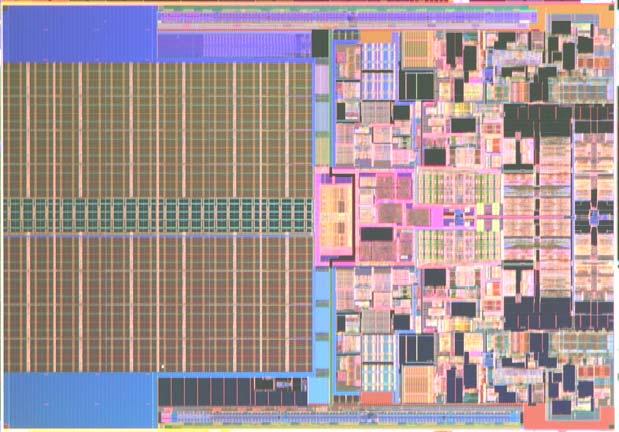
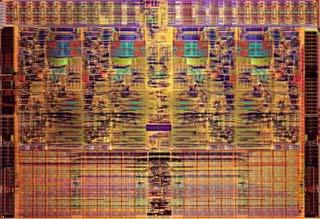
42 Multiple Microprocessors Single Core Quad Core Dual Core 33
43 Defect Reduction Trend Mature yield demonstrated 2 years after 65 nm 130 nm 90 nm 65 nm 45 nm Defect Density (log scale)
44 Defect Reduction Trend Mature yield demonstrated 2 years after 65 nm Matched yield in 2 ND Fab Copy Exactly! 130 nm 90 nm 65 nm 45 nm Defect Density (log scale) F
45 Conclusions A 45 nm technology is described with Design rules supporting ~2X improvement in transistor density 193nm dry lithography at critical layers for low cost Trench contacts supporting local routing 8 standard Cu interconnect layers with extensive use of low-k Thick Metal 9 Cu RDL with polymer ILD High-k + Metal gate transistors implemented for the first time in a high volume manufacturing process Integrated with 3 RD generation strained silicon Achieve record drive currents at low I OFF and tight gate pitch The technology is already in high volume manufacturing High yields demonstrated on SRAM and 3 microprocessors High yields demonstrated in two 300mm fabs 35
46 Acknowledgements The authors gratefully acknowledge the many people in the following organizations at Intel who contributed to this work: Portland Technology Development Quality and Reliability Engineering Process & Technology Modeling Assembly & Test Technology Development 36
47 For further information on Intel's silicon technology, please visit our Technology & Research page at 37
High Performance High-K + Metal Gate Strain Enhanced Transistors on (110) Silicon
 Silicon") High Performance High-K + Metal Gate Strain Enhanced Transistors on (110) Silicon Paul Packan, S. Cea*, H. Deshpande, T. Ghani, M. Giles*, O. Golonzka, M. Hattendorf, R. Kotlyar*, K. Kuhn, A. Murthy, P.
High Performance High-K + Metal Gate Strain Enhanced Transistors on (110) Silicon Paul Packan, S. Cea*, H. Deshpande, T. Ghani, M. Giles*, O. Golonzka, M. Hattendorf, R. Kotlyar*, K. Kuhn, A. Murthy, P.
Mark T. Bohr Intel Senior Fellow, Technology and Manufacturing Group Director, Process Architecture and Integration INTEL CORPORATION
 Mark T. Bohr Intel Senior Fellow, Technology and Manufacturing Group Director, Process Architecture and Integration INTEL CORPORATION Patents» 6762464, N-P butting connections on SOI substrates, 7/13/2004.»
Tri-Gate Transistor Architecture with High-k Gate Dielectrics, Metal Gates and Strain Engineering
 Tri-Gate Transistor Architecture with High-k Gate Dielectrics, Metal Gates and Strain Engineering Jack Kavalieros, Brian Doyle, Suman Datta, Gilbert Dewey, Mark Doczy, Ben Jin, Dan Lionberger, Matthew
Complementary Metal Oxide Semiconductor (CMOS)
") Technische Universität Graz Institute of Solid State Physics Complementary Metal Oxide Semiconductor (CMOS) Franssila: Chapters 26,28 Technische Universität Graz Institute of Solid State Physics Complementary
Technische Universität Graz Institute of Solid State Physics Complementary Metal Oxide Semiconductor (CMOS) Franssila: Chapters 26,28 Technische Universität Graz Institute of Solid State Physics Complementary
A New High-k Transistor Technology Implemented in Accordance with the 55nm Design Rule Process
 A New High-k Transistor Technology Implemented in Accordance with the 55nm Design Rule Process FUKASE Tadashi, NAKAHARA Yasushi, TAKAHASHI Toshifumi, IMAI Kiyotaka Abstract NEC Electronics has developed
Hafnium -based gate dielectrics for high performance logic CMOS applications
 Hafnium -based gate dielectrics for high performance logic CMOS applications T. Kelwing*, M. Trentzsch, A. Naumann, B. Bayha, B. Trui, L. Herrmann, F. Graetsch, R. Carter, R. Stephan, P. Kuecher & W. Hansch
CMOS Technology. Flow varies with process types & company. Start with substrate selection. N-Well CMOS Twin-Well CMOS STI
 CMOS Technology Flow varies with process types & company N-Well CMOS Twin-Well CMOS STI Start with substrate selection Type: n or p Doping level, resistivity Orientation, 100, or 101, etc Other parameters
Lecture 2: CMOS Fabrication Mark McDermott Electrical and Computer Engineering The University of Texas at Austin
 Lecture 2: CMOS Fabrication Mark McDermott Electrical and Computer Engineering The University of Texas at Austin Agenda Last module: Introduction to the course How a transistor works CMOS transistors This
MOS Front-End. Field effect transistor
 MOS Front-End Back-end Transistor Contact Front-end p-well STI n-well Front-end-of-line includes substrate, isolation, wells, transistor, silicide Field effect transistor MOSFET: Metal-Oxide-Semiconductor
EE 143 FINAL EXAM NAME C. Nguyen May 10, Signature:
 INSTRUCTIONS Read all of the instructions and all of the questions before beginning the exam. There are 5 problems on this Final Exam, totaling 143 points. The tentative credit for each part is given to
VLSI Design and Simulation
 VLSI Design and Simulation CMOS Processing Technology Topics CMOS Processing Technology Semiconductor Processing How do we make a transistor? Fabrication Process Wafer Processing Silicon single crystal
Reliability Challenges for 45nm and Beyond. J. W. McPherson, PhD, TI Senior Fellow Texas Instruments, Inc. Dallas, Texas 75243
 Reliability Challenges for 45nm and Beyond J. W. McPherson, PhD, TI Senior Fellow Texas Instruments, Inc. Dallas, Texas 75243 DAC 2006 1 2 Outline Transistor Performance with Scaling Gate Dielectric Scaling
ECE321 Electronics I
 ECE321 Electronics I Lecture 19: CMOS Fabrication Payman Zarkesh-Ha Office: ECE Bldg. 230B Office hours: Tuesday 2:00-3:00PM or by appointment E-mail: payman@ece.unm.edu Slide: 1 Miller Effect Interconnect
Microelectronics. Integrated circuits. Introduction to the IC technology M.Rencz 11 September, Expected decrease in line width
 Microelectronics Introduction to the IC technology M.Rencz 11 September, 2002 9/16/02 1/37 Integrated circuits Development is controlled by the roadmaps. Self-fulfilling predictions for the tendencies
Layout-related stress effects on TID-induced leakage current
 Layout-related stress effects on TID-induced leakage current Nadia Rezzak, R. D. Schrimpf, M. L. Alles, En Xia Zhang, Daniel M. Fleetwood, Yanfeng Albert Li Radiation Effects Group Vanderbilt University,
ECE520 VLSI Design. Lecture 7: CMOS Manufacturing Process. Payman Zarkesh-Ha
 ECE520 VLSI Design Lecture 7: CMOS Manufacturing Process Payman Zarkesh-Ha Office: ECE Bldg. 230B Office hours: Wednesday 2:00-3:00PM or by appointment E-mail: pzarkesh@unm.edu Slide: 1 Review of Last
VLSI Systems and Computer Architecture Lab
 ΚΥΚΛΩΜΑΤΑ VLSI Πανεπιστήμιο Ιωαννίνων CMOS Technology Τμήμα Μηχανικών Η/Υ και Πληροφορικής 1 From the book: An Introduction ti to VLSI Process By: W. Maly ΚΥΚΛΩΜΑΤΑ VLSI Διάρθρωση 1. N well CMOS 2. Active
New Materials as an enabler for Advanced Chip Manufacturing
 New Materials as an enabler for Advanced Chip Manufacturing Drive Innovation, Deliver Excellence ASM International Analyst and Investor Technology Seminar Semicon West July 10 2013 Outline New Materials:
Silicon Wafer Processing PAKAGING AND TEST
 Silicon Wafer Processing PAKAGING AND TEST Parametrical test using test structures regularly distributed in the wafer Wafer die test marking defective dies dies separation die fixing (not marked as defective)
Cleaning Trends for Advanced Nodes. April 9, 2018 Scotten W. Jones President IC Knowledge LLC
 Cleaning Trends for Advanced Nodes April 9, 2018 Scotten W. Jones President IC Knowledge LLC sjones@icknowledge.com Outline DRAM Logic NAND Conclusion 2 DRAM Nodes 2011 2012 2013 2014 2015 2016 2017 2018
Evaluation and Evolution of Low κ Inter-Layer Dielectric (ILD) Material and Integration Schemes
 Material and Integration Schemes") Evaluation and Evolution of Low κ Inter-Layer Dielectric (ILD) Material and Integration Schemes Dr Eb Andideh Intel Corporation Logic Technology Development Contact: ebrahimandideh@intelcom 1 Disclaimer
Evaluation and Evolution of Low κ Inter-Layer Dielectric (ILD) Material and Integration Schemes Dr Eb Andideh Intel Corporation Logic Technology Development Contact: ebrahimandideh@intelcom 1 Disclaimer
Microelectronic Engineering
 Microelectronic Engineering 86 (2009) 1728 1732 Contents lists available at ScienceDirect Microelectronic Engineering journal homepage: www.elsevier.com/locate/mee Flat band voltage control on low V t
THERMAL OXIDATION - Chapter 6 Basic Concepts
 THERMAL OXIDATION - Chapter 6 Basic Concepts SiO 2 and the Si/SiO 2 interface are the principal reasons for silicon s dominance in the IC industry. Oxide Thickness µm 0. µm 0 nm nm Thermally Grown Oxides
Contact Resistance Reduction using Advanced Implant and Anneal Techniques for 7nm Node and Beyond
 Contact Resistance Reduction using Advanced Implant and Anneal Techniques for 7nm Node and Beyond Fareen Adeni Khaja Global Product Manager, Front End Products Transistor and Interconnect Group NCCAVS
MOS Gate Dielectrics. Outline
 MOS Gate Dielectrics Outline Scaling issues Technology Reliability of SiO 2 Nitrided SiO 2 High k dielectrics 42 Incorporation of N or F at the Si/SiO 2 Interface Incorporating nitrogen or fluorine instead
EEC 118 Lecture #5: MOS Fabrication. Rajeevan Amirtharajah University of California, Davis Jeff Parkhurst Intel Corporation
 EEC 118 Lecture #5: MOS Fabrication Rajeevan Amirtharajah University of California, Davis Jeff Parkhurst Intel Corporation Announcements Lab 3 this week, report due next week HW 3 due this Friday at 4
Chapter 3 Silicon Device Fabrication Technology
 Chapter 3 Silicon Device Fabrication Technology Over 10 15 transistors (or 100,000 for every person in the world) are manufactured every year. VLSI (Very Large Scale Integration) ULSI (Ultra Large Scale
Chapter 2 Manufacturing Process
 Digital Integrated Circuits A Design Perspective Chapter 2 Manufacturing Process 1 CMOS Process 2 CMOS Process (n-well) Both NMOS and PMOS must be built in the same silicon material. PMOS in n-well NMOS
VLSI INTRODUCTION P.VIDYA SAGAR ( ASSOCIATE PROFESSOR) Department of Electronics and Communication Engineering, VBIT
 Department of Electronics and Communication Engineering, VBIT") VLSI INTRODUCTION P.VIDYA SAGAR ( ASSOCIATE PROFESSOR) contents UNIT I INTRODUCTION: Introduction to IC Technology MOS, PMOS, NMOS, CMOS & BiCMOS technologies. BASIC ELECTRICAL PROPERTIES : Basic Electrical
VLSI INTRODUCTION P.VIDYA SAGAR ( ASSOCIATE PROFESSOR) contents UNIT I INTRODUCTION: Introduction to IC Technology MOS, PMOS, NMOS, CMOS & BiCMOS technologies. BASIC ELECTRICAL PROPERTIES : Basic Electrical
PROCESS FLOW AN INSIGHT INTO CMOS FABRICATION PROCESS
 Contents: VI Sem ECE 06EC63: Analog and Mixed Mode VLSI Design PROCESS FLOW AN INSIGHT INTO CMOS FABRICATION PROCESS 1. Introduction 2. CMOS Fabrication 3. Simplified View of Fabrication Process 3.1 Alternative
CMP challenges in sub-14nm FinFET and RMG technologies
 CMP challenges in sub-14nm FinFET and RMG technologies Tae Hoon Lee*, Hong Jin Kim, Venugopal Govindarajulu, Gerett Yocum & Jason Mazzotti Advanced Module Engineering NCCAVS CMPUG Spring Meeting 2016 Contents
CMOS Processing Technology
 CHAPTER 2 CMOS Processing Technology Outline 2 1. CMOS Technologies 2. Layout Design Rules 3. CMOS Process Enhancements 4. Technology-related CAD Issues 5. Manufacturing Issues CMOS Technologies 3 n-well
1 Thin-film applications to microelectronic technology
 1 Thin-film applications to microelectronic technology 1.1 Introduction Layered thin-film structures are used in microelectronic, opto-electronic, flat panel display, and electronic packaging technologies.
Making of a Chip Illustrations
 Making of a Chip Illustrations 22nm 3D/Trigate Transistors Version April 2015 1 The illustrations on the following foils are low resolution images that visually support the explanations of the individual
EE40 Lec 22. IC Fabrication Technology. Prof. Nathan Cheung 11/19/2009
 Suggested Reading EE40 Lec 22 IC Fabrication Technology Prof. Nathan Cheung 11/19/2009 300mm Fab Tour http://www-03.ibm.com/technology/manufacturing/technology_tour_300mm_foundry.html Overview of IC Technology
Fairchild Semiconductor Application Note June 1983 Revised March 2003
 Fairchild Semiconductor Application Note June 1983 Revised March 2003 High-Speed CMOS (MM74HC) Processing The MM74HC logic family achieves its high speed by utilizing microcmos Technology. This is a 3.5
Advanced CMOS Process Technology Part 3 Dr. Lynn Fuller
 MICROELECTRONIC ENGINEERING ROCHESTER INSTITUTE OF TECHNOLOGY Part 3 Dr. Lynn Fuller Webpage: http://people.rit.edu/lffeee Electrical and Microelectronic Engineering Rochester Institute of Technology 82
Annual Meeting. North Carolina State University Dr. Veena Misra. January 17 19, 2017 December
 Annual Meeting North Carolina State University Dr. Veena Misra January 17 19, 2017 December 8 2015 1 Misra Group at NCSU Over 9 years experience in wide band gap research on SiC, GaN and Ga2O3. World leaders
Performance Predictions for Scaled Process-induced Strained-Si CMOS
 Performance Predictions for Scaled Process-induced Strained-Si CMOS G Ranganayakulu and C K Maiti Department of Electronics and ECE, IIT Kharagpur, Kharagpur 721302, India Abstract: Device and circuit
Strain for CMOS performance Improvement
 IBM Corporation Strain for CMOS performance Improvement +Victor Chan, +Ken Rim, #Meikei Ieong, +Sam Yang, +Rajeev Malik, Young Way Teh, #Min Yang, #Qiqing (Christine) Ouyang +IBM Systems & Technology Group,
RECONFIGURABLE NEUROMORPHIC SYNAPSE INTERCONNECTS WITH TFT
 RECONFIGURABLE NEUROMORPHIC SYNAPSE INTERCONNECTS WITH TFT JAN GENOE PUBLIC Every neuron in a human brain is connected via its synapses to 10-15.000 other neurons. Those connections can be over time reconfigured
Development of a Deep-Submicron CMOS Process for Fabrication of High Performance 0.25 mm Transistors
 Development of a Deep-Submicron CMOS Process for Fabrication of High Performance 0.25 mm Transistors Michael Aquilino M.S. Thesis Defense Department May 19, 2006 Motivation o Enable the department to continue
The Journey to FinFETs
 The Journey to FinFETs Alvin Loke 30-Apr-2015 Qualcomm Learning Center The 10000-Foot View A Switch small, fast, thrifty Scaling Performance Energy-Efficient Slide 1 CMOS Scaling Still Alive Intel 22nm
CMOS Processing Technology
 CHAPTER 2 CMOS Processing Technology Outline 2 1. CMOS Technologies 2. Layout Design Rules 3. CMOS Process Enhancements 4. Technology-related CAD Issues 5. Manufacturing Issues CMOS Technologies 3 n-well
The History & Future of
 The History & Future of CMP CMPUG July 2008 Karey Holland, Ph.D. kholland@nexplanar.com Ken Cadien, Ph.D. University of Alberta kcadien@ualberta.ca http://www.nexplanar.com http://www.ualberta.ca/ Outline
6.774 Fall 2006: Global and Local Stress to Enhance CMOS Performance
 6.774 Fall 2006: Global and Local Stress to Enhance CMOS Performance techniques have been developed to strain the Si in the MOSFET channel, in order to enhance carrier mobility and current drive some of
EE 330 Lecture 9. IC Fabrication Technology Part II. -Oxidation -Epitaxy -Polysilicon -Planarization -Resistance and Capacitance in Interconnects
 EE 330 Lecture 9 IC Fabrication Technology Part II -Oxidation -Epitaxy -Polysilicon -Planarization -Resistance and Capacitance in Interconnects Review from Last Time Etching Dry etch (anisotropic) SiO
CMOS FABRICATION. n WELL PROCESS
 CMOS FABRICATION n WELL PROCESS Step 1: Si Substrate Start with p- type substrate p substrate Step 2: Oxidation Exposing to high-purity oxygen and hydrogen at approx. 1000 o C in oxidation furnace SiO
EE THERMAL OXIDATION - Chapter 6. Basic Concepts
 EE 22 FALL 999-00 THERMAL OXIDATION - Chapter 6 Basic Concepts SiO 2 and the Si/SiO 2 interface are the principal reasons for silicon s dominance in the IC industry. SiO 2 : Easily selectively etched using
Manufacturer Part Number. Module 2: CMOS FEOL Analysis
 Manufacturer Part Number description Module 2: CMOS FEOL Analysis Manufacturer Device # 2 Some of the information is this report may be covered by patents, mask and/or copyright protection. This report
Overview of Dual Damascene Cu/Low-k Interconnect
 ERC Retreat Stanford: New Chemistries & Tools for scco 2 Processing of Thin Films Overview of Dual Damascene Cu/Low-k Interconnect P. Josh Wolf 1,4 - Program Manager, Interconnect Div. josh.wolf@sematech.org
CS/ECE 5710/6710. N-type Transistor. N-type from the top. Diffusion Mask. Polysilicon Mask. CMOS Processing
 CS/ECE 5710/6710 CMOS Processing Addison-Wesley N-type Transistor D G +Vgs + Vds S N-type from the top i electrons - Diffusion Mask Mask for just the diffused regions Top view shows patterns that make
Copper Interconnect Technology
 Tapan Gupta Copper Interconnect Technology i Springer Contents 1 Introduction 1 1.1 Trends and Challenges 2 1.2 Physical Limits and Search for New Materials 5 1.3 Challenges 6 1.4 Choice of Materials 7
Motorola PC603R Microprocessor
 Construction Analysis Motorola PC603R Microprocessor Report Number: SCA 9709-551 Global Semiconductor Industry the Serving Since 1964 17350 N. Hartford Drive Scottsdale, AZ 85255 Phone: 602-515-9780 Fax:
EE 434 Lecture 9. IC Fabrication Technology
 EE 434 Lecture 9 IC Fabrication Technology Quiz 7 The layout of a film resistor with electrodes A and B is shown. If the sheet resistance of the film is 40 /, determine the resistance between nodes A and
Chapter 4 : ULSI Process Integration (0.18 m CMOS Process)
") Chapter : ULSI Process Integration (0.8 m CMOS Process) Reference. Semiconductor Manufacturing Technology : Michael Quirk and Julian Serda (00). - (00). Semiconductor Physics and Devices- Basic Principles(/e)
Chapter : ULSI Process Integration (0.8 m CMOS Process) Reference. Semiconductor Manufacturing Technology : Michael Quirk and Julian Serda (00). - (00). Semiconductor Physics and Devices- Basic Principles(/e)
KGC SCIENTIFIC Making of a Chip
 KGC SCIENTIFIC www.kgcscientific.com Making of a Chip FROM THE SAND TO THE PACKAGE, A DIAGRAM TO UNDERSTAND HOW CPU IS MADE? Sand CPU CHAIN ANALYSIS OF SEMICONDUCTOR Material for manufacturing process
Highly Reliable Low Temperature Ultrathin Oxides Grown Using N 2 O Plasma
 Highly Reliable Low Temperature Ultrathin Oxides Grown Using N 2 O Plasma Jam-Wem Lee 1, Yiming Li 1,2, and S. M. Sze 1,3 1 Department of Nano Device Technology, National Nano Device Laboratories, Hsinchu,
Atomic Level Material and Device Analysis for FinFET and Nanowire Design
 Atomic Level Material and Device Analysis for FinFET and Nanowire Design Victor Moroz, Søren Smidstrup, Munkang Choi, and Alexei Svizhenko July 13, Junction Technologies User Group Meeting 2018 Synopsys,
Process Uniformity Improvements for LSA Millisecond Annealing in the FinFET era Jim McWhirter, Ph.D. July 16, 2015
 1 NCCAVS Junction Technology Group SEMICON West 2015 Meeting July 16, 2015 Process Uniformity Improvements for LSA Millisecond Annealing in the FinFET era Jim McWhirter, Ph.D. July 16, 2015 DEVICE PERFORMANCE
2006 UPDATE METROLOGY
 INTERNATIONAL TECHNOLOGY ROADMAP FOR SEMICONDUCTORS METROLOGY THE ITRS DEVED AND INTENDED FOR TECHNOLOGY ASSESSMENT ONLY AND WITHOUT REGARD TO ANY COMMERCIAL CONSIDERATIONS PERTAINING TO INDIVIDUAL PRODUCTS
ECE 659. Jan M. Rabaey Anantha Chandrakasan Borivoje Nikolic. July 30, Digital EE141 Integrated Circuits 2nd Manufacturing.
 Digital Integrated Circuits A Design Perspective Jan M. Rabaey Anantha Chandrakasan Borivoje Nikolic Manufacturing Process July 0, 00 1 CMOS Process 1 A Modern CMOS Process gate-oxide TiSi AlCu Tungsten
Manufacturing Process
 Manufacturing Process 1 CMOS Process 2 A Modern CMOS Process gate-oxide TiSi 2 AlCu Tungsten SiO 2 n+ p-well p-epi poly n-well p+ SiO 2 p+ Dual-Well Trench-Isolated CMOS Process 3 Single-crystal ingot
Cost of Integrated Circuits
 Cost of IC Design 1 Cost of Integrated Circuits NRE (Non-Recurrent Engineering) costs fixed design time and effort, mask generation independent of sales volume / number of products one-time cost factor
Lecture #18 Fabrication OUTLINE
 Transistors on a Chip Lecture #18 Fabrication OUTLINE IC Fabrication Technology Introduction the task at hand Doping Oxidation Thin-film deposition Lithography Etch Lithography trends Plasma processing
IME Technical Proposal. High Density FOWLP for Mobile Applications. 22 April High Density FOWLP Consortium Forum
 IME Technical Proposal High Density FOWLP for Mobile Applications 22 April 2014 Packaging driver for portable / mobile applications Key drivers/needs Smaller form-factor lower profile, substrate-less Higher
MOLYBDENUM AS A GATE ELECTRODE FOR DEEP SUB-MICRON CMOS TECHNOLOGY
 Mat. Res. Soc. Symp. Vol. 611 2000 Materials Research Society MOLYBDENUM AS A GATE ELECTRODE FOR DEEP SUB-MICRON CMOS TECHNOLOGY Pushkar Ranade, Yee-Chia Yeo, Qiang Lu, Hideki Takeuchi, Tsu-Jae King, Chenming
FABRICATION of MOSFETs
 FABRICATION of MOSFETs CMOS fabrication sequence -p-type silicon substrate wafer -creation of n-well regions for pmos transistors, -impurity implantation into the substrate. -thick oxide is grown in the
Lecture 22: Integrated circuit fabrication
 Lecture 22: Integrated circuit fabrication Contents 1 Introduction 1 2 Layering 4 3 Patterning 7 4 Doping 8 4.1 Thermal diffusion......................... 10 4.2 Ion implantation.........................
This Appendix discusses the main IC fabrication processes.
 IC Fabrication B B.1 Introduction This Appendix discusses the main IC fabrication processes. B.2 NMOS fabrication NMOS transistors are formed in a p-type substrate. The NMOS fabrication process requires
Impact of the source/drain implants on threshold voltage matching in deep submicron CMOS technologies
 Impact of the source/drain implants on threshold voltage matching in deep submicron CMOS technologies Jerôme Dubois 1, Johan Knol 1, Hans Tuinhout 2, Jurriaan Schmitz 2, Peter Stolk 2 and Mike Bolt 1 1
Interconnects OUTLINE
 Interconnects 1 Interconnects OUTLINE 1. Overview of Metallization 2. Introduction to Deposition Methods 3. Interconnect Technology 4. Contact Technology 5. Refractory Metals and their Silicides Reading:
Implant And Annealing Process Integration Issues To Reduce Device Variability For <10nm p+ & n+ Ultra-Shallow junctions
 Implant And Annealing Process Integration Issues To Reduce Device Variability For
Introduction to CMOS VLSI Design. Layout, Fabrication, and Elementary Logic Design
 Introduction to CMOS VLSI Design Layout, Fabrication, and Elementary Logic Design CMOS Fabrication CMOS transistors are fabricated on silicon wafer Lithography process similar to printing press On each
Graduate Student Presentations
 Graduate Student Presentations Dang, Huong Chip packaging March 27 Call, Nathan Thin film transistors/ liquid crystal displays April 4 Feldman, Ari Optical computing April 11 Guerassio, Ian Self-assembly
Problem 1 Lab Questions ( 20 points total)
") Problem 1 Lab Questions ( 20 points total) (a) (3 points ) In our EE143 lab, we use Phosphorus for the source and drain diffusion. However, most advanced processes use Arsenic. What is the advantage of
Problem 1 Lab Questions ( 20 points total) (a) (3 points ) In our EE143 lab, we use Phosphorus for the source and drain diffusion. However, most advanced processes use Arsenic. What is the advantage of
Manufacturing Process
 Digital Integrated Circuits A Design Perspective Jan M. Rabaey Anantha Chandrakasan Borivoje Nikolic Manufacturing Process July 30, 2002 1 CMOS Process 2 A Modern CMOS Process gate-oxide TiSi 2 AlCu Tungsten
A Production-Proven Shallow Trench Isolation (STI) Solution Using Novel CMP Concepts*
 Solution Using Novel CMP Concepts*") A Production-Proven Shallow Trench Isolation (STI) Solution Using Novel CMP Concepts* Raymond R. Jin, Jeffrey David, Bob Abbassi, Tom Osterheld, Fritz Redeker Applied Materials, 3111 Coronado Drive, M/S
A Production-Proven Shallow Trench Isolation (STI) Solution Using Novel CMP Concepts* Raymond R. Jin, Jeffrey David, Bob Abbassi, Tom Osterheld, Fritz Redeker Applied Materials, 3111 Coronado Drive, M/S
EE 330 Lecture 9. IC Fabrication Technology Part II. -Oxidation -Epitaxy -Polysilicon -Planarization -Resistance and Capacitance in Interconnects
 EE 330 Lecture 9 IC Fabrication Technology Part II -Oxidation -Epitaxy -Polysilicon -Planarization -Resistance and Capacitance in Interconnects Review from Last Time IC Fabrication Technology Crystal Preparation
Application of Taguchi Method in Optimization of Gate Oxide and Silicide Thickness for 45nm NMOS Device
 International Journal of Engineering & Technology IJET-IJENS Vol:09 No:10 72 Application of Taguchi Method in Optimization of Gate Oxide and Silicide Thickness for 45nm NMOS Device Fauziyah Salehuddin
CMOS Fabrication. Dr. Bassam Jamil. Adopted from slides of the textbook
 CMOS Fabrication Dr. Bassam Jamil Adopted from slides of the textbook CMOS Fabrication CMOS transistors are fabricated on silicon wafer Lithography process similar to printing press On each step, different
Effect of annealing temperature on the electrical properties of HfAlO thin films. Chun Lia, Zhiwei Heb*
 International Forum on Energy, Environment and Sustainable Development (IFEESD 2016) Effect of annealing temperature on the electrical properties of HfAlO thin films Chun Lia, Zhiwei Heb* Department of
Motorola MC68360EM25VC Communication Controller
 Construction Analysis EM25VC Communication Controller Report Number: SCA 9711-562 Global Semiconductor Industry the Serving Since 1964 17350 N. Hartford Drive Scottsdale, AZ 85255 Phone: 602-515-9780 Fax:
Lecture 19 Microfabrication 4/1/03 Prof. Andy Neureuther
 EECS 40 Spring 2003 Lecture 19 Microfabrication 4/1/03 Prof. ndy Neureuther How are Integrated Circuits made? Silicon wafers Oxide formation by growth or deposition Other films Pattern transfer by lithography
X-Ray Reflectivity Study of Hafnium Silicate Thin Films Prepared by Thermal Chemical Vapor Deposition
 X-Ray Reflectivity Study of Hafnium Silicate Thin Films Prepared by Thermal Chemical Vapor Deposition Hideyuki YAMAZAKI, Advanced LSI Technology Laboratory, Toshiba Corporation hideyuki.yamazaki@toshiba.co.jp
Atomic Layer Deposition of High-k k Dielectric and Metal Gate Stacks for MOS Devices
 International Conference on Characterization and Metrology for ULSI Technology March 15-18, 2005 Atomic Layer Deposition of High-k k Dielectric and Metal Gate Stacks for MOS Devices Yoshi Senzaki, Kisik
EE 330 Lecture 12. Devices in Semiconductor Processes
 EE 330 Lecture 12 Devices in Semiconductor Processes Review from Lecture 9 Copper Interconnects Limitations of Aluminum Interconnects Electromigration Conductivity not real high Relevant Key Properties
UT Austin, ECE Department VLSI Design 2. CMOS Fabrication, Layout Rules
 2. CMOS Fabrication, Layout, Design Rules Last module: Introduction to the course How a transistor works CMOS transistors This module: CMOS Fabrication Design Rules CMOS Fabrication CMOS transistors are
Characterization and Fabrication of 90nm Strained Silicon PMOS using TCAD
 Characterization and Fabrication of 90nm Strained Silicon PMOS using TCAD M. A. Abd Hamid and F. Sulaiman, Member, IEEE Abstract The paper focuses on the enhancement of conventional 90nm PMOS using graded
Czochralski Crystal Growth
 Czochralski Crystal Growth Crystal Pulling Crystal Ingots Shaping and Polishing 300 mm wafer 1 2 Advantage of larger diameter wafers Wafer area larger Chip area larger 3 4 Large-Diameter Wafer Handling
Complementary Metal-Oxide-Semiconductor Very Large-Scale Integrated Circuit Design
 Complementary Metal-Oxide-Semiconductor Very Large-Scale Integrated Circuit Design Bradley A. Minch Mixed Analog-Digital VLSI Circuits and Systems Lab Cornell University Ithaca, NY 14853 5401 minch@ece.cornell.edu
Semiconductor Manufacturing Technology. IC Fabrication Process Overview
 Semiconductor Manufacturing Technology Michael Quirk & Julian Serda October 00 by Prentice Hall Chapter 9 IC Fabrication Process Overview /4 Objectives After studying the material in this chapter, you
TSMC Property. ConFab. Bridging the Fabless-Foundry Gap. BJ Woo. Sr. Director Business Development TSMC TSMC, Ltd
 ConFab Bridging the Fabless-Foundry Gap BJ Woo Sr. Director Business Development TSMC 2 Outline Fabless Requirements Technology Scaling Challenges IP Quality Foundry Integrated Manufacturing Value Summary
CSCI 4974 / 6974 Hardware Reverse Engineering. Lecture 5: Fabrication processes
 CSCI 4974 / 6974 Hardware Reverse Engineering Lecture 5: Fabrication processes QUIZ 3: CMOS layout Quiz Discussion Rationale If you know how something is put together, you can figure out how to take it
Amorphous and Polycrystalline Thin-Film Transistors
 Part I Amorphous and Polycrystalline Thin-Film Transistors HYBRID AMORPHOUS AND POLYCRYSTALLINE SILICON DEVICES FOR LARGE-AREA ELECTRONICS P. Mei, J. B. Boyce, D. K. Fork, G. Anderson, J. Ho, J. Lu, Xerox
IC Fabrication Technology Part III Devices in Semiconductor Processes
 EE 330 Lecture 10 IC Fabrication Technology Part III Metalization and Interconnects Parasitic Capacitances Back-end Processes Devices in Semiconductor Processes Resistors Diodes Review from Last Lecture
Strained Silicon-On-Insulator Fabrication and Characterization
 10.1149/1.2728880, The Electrochemical Society Strained Silicon-On-Insulator Fabrication and Characterization M. Reiche a, C. Himcinschi a, U. Gösele a, S. Christiansen a, S. Mantl b, D. Buca b, Q.T. Zhao
TSV Processing and Wafer Stacking. Kathy Cook and Maggie Zoberbier, 3D Business Development
 TSV Processing and Wafer Stacking Kathy Cook and Maggie Zoberbier, 3D Business Development Outline Why 3D Integration? TSV Process Variations Lithography Process Results Stacking Technology Wafer Bonding
EECS130 Integrated Circuit Devices
 EECS130 Integrated Circuit Devices Professor Ali Javey 9/13/2007 Fabrication Technology Lecture 1 Silicon Device Fabrication Technology Over 10 15 transistors (or 100,000 for every person in the world)
Process Optimization in Post W CMP In-situ Cleaning. Hong Jin Kim, Si-Gyung Ahn, Liqiao Qin CMP, Advanced Module Engineering GLOBALFOUNDRIES, USA
 Process Optimization in Post W CMP In-situ Cleaning Hong Jin Kim, Si-Gyung Ahn, Liqiao Qin CMP, Advanced Module Engineering GLOBALFOUNDRIES, USA Contents W CMP process for sub 14nm device W Gate CMP W