National Semiconductor LM2672 Simple Switcher Voltage Regulator
|
|
|
- Isabel Audrey Park
- 6 years ago
- Views:
Transcription
1 Construction Analysis National Semiconductor LM2672 Simple Switcher Voltage Regulator Report Number: SCA Global Semiconductor Industry the Serving Since N. Hartford Drive Scottsdale, AZ Phone: Fax: Internet:
2 INDEX TO TEXT TITLE PAGE INTRODUCTION 1 MAJOR FINDINGS 1 TECHNOLOGY DESCRIPTION Assembly 2 Die Process and Design 2-3 ANALYSIS RESULTS I Assembly 4 ANALYSIS RESULTS II Die Process and Design 5-7 TABLES Procedure 8 Overall Quality Evaluation 9 Package Markings 10 Wirebond Strength 10 Die Material Analysis 10 Horizontal Dimensions 11 Vertical Dimensions 12 i
3 INTRODUCTION This report describes a construction analysis of the National Semiconductor LM2672 Simple Switcher voltage regulator. Five devices were supplied, encapsulated in 8-pin Dual-In-Line plastic packages (DIP). Date codes were not identifiable. MAJOR FINDINGS Questionable Items: 1 Metal cracks were noted at contact edges. Significant silicon in contacts. Special Features: Linear Power BiCMOS process which includes a double diffused (DMOS) process. Extended shallow source/drain N-channel transistor structure. Design Features: Large area for double diffused (DMOS) process. Large capacitor structures. 1 These items present possible quality or reliability concerns. They should be discussed with the manufacturer to determine their possible impact on the intended application
4 TECHNOLOGY DESCRIPTION Assembly: Devices were encapsulated in 8-pin plastic DIPs. Lead-locking provisions (anchors and holes) were present at all pins. Thermosonic ball bond method employing 1.3 mil O.D. gold wire. Silver-filled polyimide die attach. Sawn dicing (full depth). Die Process and Design Fabrication process: Linear Power BiCMOS process with N-epi, P-well, P+ iso, and N+ buried layer, incorporating N and P channel MOS, DMOS, NPN and PNP transistors. Final passivation: Two layers of passivation were employed. A layer of nitride over a layer of silicon-dioxide. Metallization: Two levels of silicon-doped aluminum defined by dry-etch techniques. No caps or barriers were present. Standard contacts and vias (no plugs). In the DMOS area metal 2 was placed directly on metal 1. Intermetal Dielectric (IMD): Intermetal dielectric consisted of single layer of glass. No planarization technique was used. Pre-metal glass: A single layer of reflow glass was used. Reflow was done prior to contact cuts. Grown and densified oxides were also present
5 TECHNOLOGY DESCRIPTION (continued) Polysilicon: Single layer of dry-etched polysilicon (no silicide) was used to form all MOS gates on the die. It was also used as the top plate for the thin oxide capacitors. An LDD process was used with spacers removed. DMOS devices: A double diffused Hexfet style process was employed. N+ diffusions formed the sources of the transistor elements. Deep P+ diffusions formed the body and inherent body diode. N- epi/buried layer formed the drain. CMOS devices: Standard N+ and P+ implanted diffusions formed the sources/drains for these transistors. Sidewall spacers were selectively used and removed. Long shallow N+ LDD extensions were present on one side of some of the NMOS transistors. P-wells and N-epi were used for N-channel devices. Bipolar devices: Standard N+ diffusions were used for emitters and collectors of NPN s and base contacts of PNP devices. The standard base diffusions also used a shallow P+ implant (probably the S/D P+) at contact areas. P+ isolation diffusions were diffused from top and bottom of the epi (to reduce isolation width). No buried contacts were employed
6 ANALYSIS RESULTS I Assembly: Figures 1-4a Note: Package analysis was not required. The following data was obtained by observation and is given here as general information. Questionable Items: 1 None. General Items: Devices were packages in 8-pin plastic DIPs. Package markings were clear and easy to read. Date codes were not identifiable. Overall package quality: Normal. No defects were noted on the external portions of the package. Deflash was of normal quality and workmanship. Lead form was of normal quality and workmanship. No problems were found. Die placement: Die was centered and silver-filled polyimide die attach was of good quantity and quality. No problems were found. Lead-locking provisions (anchors and holes) were present at all pins. Wirebonding: Thermosonic ball bond method using 1.3 mil O.D. gold wire. No bond lifts occurred and bond pull strengths were good (see page 8). Metal 2 on 1 formed the bond pads. Wire spacing and placement was good. Probe mark damage was noted at some test pads. The damage decreased the metal spacing; however, no shorts were noted. Die dicing: Die separation was by full depth sawing with good quality workmanship. 1 These items present possible quality or reliability concerns. They should be discussed with the manufacturer to determine their possible impact on the intended application
7 ANALYSIS RESULTS II Die Process and Design: Figures 5-31 Questionable Items: 1 Metal cracks were noted at contact edges. Significant silicon in contacts. Special Features: Linear Power BiCMOS process which includes a double diffused (DMOS) process. Extended shallow source/drain N-channel transistor structure. Design Features: Large area for double diffused (DMOS) process. Large capacitor structures. General Items: Fabrication process: Linear Power BiCMOS process with N-epi, P-well, P+ iso, and N+ buried layer, incorporating N and P channel MOS, DMOS, NPN and PNP transistors. Design and layout: Die layout was clean and efficient. The identification number on the die was Die surface defects: None. No contamination or processing defects were noted. 1 These items present possible quality or reliability concerns. They should be discussed with the manufacturer to determine their possible impact on the intended application
8 ANALYSIS RESULTS II (continued) Final passivation: The passivation consisted of a layer of nitride over a layer of silicon-dioxide. Passivation integrity test indicated defect free passivation. Edge seal was also good. Some residual metal was noted at the die edge; however, no problems are foreseen (Figures 3 and 3a). Metallization: Two levels of metal defined by a dry-etch of normal quality. Metal consisted of silicon-doped aluminum. No cap or barrier metals were employed. Standard vias and contacts were used (no plugs). Metal defects: None. No notching of the metal layers was present. There was significant silicon mound growth in contact areas following the removal of the metal in the MOSFET area. Worst case silicon mound growth occupied up to 40 percent of contacts and is shown in Figure 24. Cracks were noted at contact edges see Figures 26, 27 and 29. Metal step coverage: No significant metal thinning occurred at vias or contacts due to the sloped contact cuts. Contacts: Contact cuts appeared to be defined by a wet-etch technique of good quality. No significant over-etching of the contacts was present. No contact pitting was present. Substrate contacts were used to bias the P-wells (Figure 19). Intermetal Dielectric (IMD): Intermetal dielectric consisted of single layer of glass. No planarization technique was used. No problems were present. Pre-metal glass: A single layer of reflow glass was used over grown oxides. No problems were found
9 ANALYSIS RESULTS II (continued) Polysilicon: Single layer of dry-etched polysilicon (no silicide) was used to form all MOS gates on the die. It was also used as the top plate for the thin oxide capacitors and gates for the DMOS structure. The LDD process used sidewall spacers which were removed. Large poly capacitor structures were used throughout entire die. No poly resistors were present. No problems were present. Isolation: N-epi islands with N+ buried layer separated by P+ isolation. There was good separation between buried layer and isolation with minimal buried layer shift. P-wells were noted in N-epi for N-channel devices. P+ isolation (up and down) diffusions were used to isolate the N-epi islands. A step in the oxide was noted at the P+ iso diffusions. DMOS devices: A double diffused process was employed. N+ diffusions formed the sources of the transistor elements. Deep P+ diffusions formed the body and inherent body diode. N- epi/n+ buried layer formed the drain. CMOS devices: Standard N+ and P+ implanted diffusions formed the sources/drains for these transistors. Some NMOS transistors used a unique LDD extension on one side of the gate. The step in the oxide would indicates this although the implant was too light to delineate. Bipolar devices: All bipolar devices were located in N-epi/N+ buried layers. Standard N+ diffusions were used for emitters and collectors of NPN s and base contacts of PNP devices. The standard base diffusions also used a shallow P+ implant (probably the S/D P+) at contact areas. P+ isolation diffusions were diffused from top and bottom of the epi (to reduce isolation width)
10 PROCEDURE The devices were subjected to the following analysis procedures: External inspection X-ray Decapsulation Internal optical inspection SEM inspection of assembly features and passivation Wirepull test Passivation integrity test Passivation removal and inspect metal 2 Delayer to metal 1 and inspect Delayer to poly and inspect poly structures and die surface Die sectioning (90 for SEM) * Measure horizontal dimensions Measure vertical dimensions Material analysis * Delineation of cross-sections is by silicon etch unless otherwise indicated
11 OVERALL QUALITY EVALUATION: Overall Rating: Normal DETAIL OF EVALUATION Package integrity N Package markings G Die placement G Die attach quality G Wire spacing G Wirebond placement G Wirebond quality G Dicing quality N Wirebond method Thermosonic ball bonds using 1.3 mil gold wire. Dicing method: Sawn (full depth) Die attach: Silver-filled polyimide Die surface integrity: Tool marks (absence): Particles (absence): Contamination (absence): Process defects (absence): General workmanship Passivation integrity Metal definition Metal integrity Contact coverage Contact registration Contact defects NP (probe damage) N N N N G N NP (cracks at contact edges) G N NP (some significant silicon mound growth) G = Good, P = Poor, N = Normal, NP = Normal/Poor - 9 -
12 PACKAGE MARKINGS Top (National logo) 66AB 2672 M3.3 Bottom none WIREBOND STRENGTH Wire material: Die pad material: 1.3 mil diameter gold Aluminum sample 4 # of wires tested: 11 Bond lifts: 0 Force to break - high: 18g - low: 17g - avg.: 17.9g - std. dev.: 0.28 DIE MATERIAL ANALYSIS Passivation: Die metallization: Intermetal dielectric: Pre-metal glass: Nitride over silicon-dioxide. Aluminum. Silicon-dioxide. Single layer of reflow glass. Grown and densified oxides were also present
13 HORIZONTAL DIMENSIONS Die size: 1.8 x 3.5 mm (73.5 x mils) Die area: 6.3 mm 2 (10,326 mils 2 ) Min pad size: Min pad window: Min metal 2 width: Min metal 2 space: Min metal 2 pitch: Min via: Min metal 1 width: Min metal 1 space: Min metal 1 pitch: Min contact: Min poly width: Min poly space: 0.13 mm x 0.13 mm (5.1 x 5.1 mils) 0.11 mm x 0.11 mm (4.4 x 4.4 mils) 7.3 microns 7.7 microns 15 microns 5.3 microns 3.4 microns 4.3 microns 7.7 microns 3 microns 3.7 microns 4.7 microns Min gate length* - (N-channel) 3.7 microns - (P-channel) 5.0 microns Min N+ emitter: Min P+ emitter: Min P+ isolation: Min edge of base to P+ iso: Min emitter to edge of base: 16 microns (round) 12 microns (round) 10 microns 12 microns 8 microns * Physical gate length
14 VERTICAL DIMENSIONS Die thickness: 0.35 mm (14 mils) Layers Passivation 2: Passivation 1: Aluminum 2: Intermetal dielectric (IMD): Aluminum 1: Pre-metal glass: Poly: Local oxide: 1.0 micron 0.45 micron 2 microns 0.95 micron 0.75 micron 0.65 micron 0.4 micron 1 micron N+ S/D diffusion: 0.6 micron P+ S/D diffusion: 0.45 micron P DMOS body: 5.5 microns P+ base (NPN): 2.8 microns N+ (DMOS): 10 microns N+ emitter and collector (NPN): 0.6 micron N- epi: 4.5 microns P-well: 5.5 microns N+ buried layer: 24 microns (from surface)
15 INDEX TO FIGURES PACKAGE ASSEMBLY Figures 1-4 DIE LAYOUT AND IDENTIFICATION Figures 5-7 PHYSICAL DIE STRUCTURES Figures 8-22 DMOS POWER HEXFET S Figures BIPOLAR DEVICES Figures TYPICAL INPUT/OUTPUT CIRCUITRY Figure 30 CROSS SECTION DRAWING Figure 31 ii

16 CB 1 8 V SW top SS SYNC V IN GND FB 4 5 ON/OFF bottom Figure 1. Package photographs and pinout of the National LM2672 device. Mag. 10x.


17 PIN 1 top side Figure 2. X-ray views of the package. Mag. 10x.


18 DIE DIE ATTACH ATTACKED DURING DECAPSULATION Mag. 200x PADDLE Mag. 750x EDGE OF PASSIVATION Mag. 1500x RESIDUAL METAL Figure 3. SEM views of dicing and edge seal. 60.

19 N-EPI P+ ISO DIE EDGE N+ BURIED LAYER Mag. 800x INTERMETAL DIELECTRIC PRE-METAL DIELECTRIC LOCOS Mag. 4000x RESIDUAL METAL Figure 3a. Optical and SEM section views of the die edge seal. PASSIVATION DIE EDGE


20 Au Au LEADFRAME Figure 4. SEM views of typical wirebonds. Mag. 500x, 60.


21 INTERMETALLIC Au BOND N-EPI P+ ISO N+ BURIED LAYER Mag. 500x Au BOND PASSIVATION IMD LOCAL OXIDE METAL 2 M2-M1 Mag. 6500x Figure 4a. Optical and SEM section views of the bond pad structure.

22 1 C B 8 V SN 8 7 V IN 7 2 SS 2 6 GND 4 SYNC 6 GND 4 FB 5 ON/OFF Figure 5. Whole die photograph of the National LM2672 device. Mag. 60x.

23 Figure 5a. Detailed optical view of the DMOS area. Mag. 100x.

24 Figure 5b. Detailed optical view of the linear device area. Mag. 100x.


25 Mag. 400x Mag. 500x Figure 6. Die identification markings from the surface. Mag. 800x Mag. 500x


26 Mag. 500x Mag. 800x Mag. 800x Figure 6a. Additional die markings from the surface.


27 Figure 7. Optical views of the die corners on the National LM2672 device. Mag. 200x.


28 Mag. 1000x Mag. 3100x Figure 8. SEM views illustrating passivation coverage. 60.


29 PASSIVATION METAL 2 Mag. 3000x POLY N+ P-WELL PASSIVATION 2 PASSIVATION 1 METAL 2 PRE-METAL GLASS IMD Si POLY Mag. 8000x LOCOS GATE OXIDE Figure 8a. SEM section views illustrating general construction. PASSIVATION 2 PASSIVATION 1 METAL 2 IMD PRE-METAL GLASS LOCOS Figure 9. SEM section view of a metal 2 line profile. Mag. 10,000x.


30 METAL 2 Mag. 500x Mag. 1000x METAL 2 METAL 2 VIA Mag. 3250x Figure 10. Topological SEM views illustrating metal 2 patterning. 0.


31 METAL 2 POLY Mag. 2000x METAL 2 Mag. 2700x Figure 11. Perspective SEM views of metal 2 coverage. 60.


32 METAL 2 POLY Figure 11a. Detailed SEM view of a metal 2-to-metal 1 via. Mag. 5000x, 60. PASSIVATION 1 PASSIVATION 2 METAL 2 Si Figure 11b. SEM section view of a metal 2-to-metal 1 via. Mag. 10,000x.


33 PASSIVATION 1 PASSIVATION 2 METAL 2 STAINING ARTIFACTS IMD PRE-METAL GLASS LOCOS Mag. 7000x PASSIVATION 1 IMD PRE-METAL GLASS Mag. 20,000x Figure 12. SEM section views of metal 1 line profiles.


34 Mag. 1000x POLY Mag. 1000x POLY METAL 2 Mag. 1300x Figure 13. Topological SEM views illustrating metal 1 patterning. 0.


35 Mag. 2400x POLY Mag. 5000x POLY POLY Mag. 6500x Figure 14. Perspective SEM views of metal 1 coverage. 60.


36 RESISTORS resistors BASE EMITTER COLLECTOR NPN transistor Figure 14a. Additional SEM views of metal 1 coverage. Mag. 1600x, 60.


37 PASSIVATION metal 1-to-N+, Mag. 10,000x N+ Si IMD metal 1-to-P+, Mag. 10,000x P+ ARTIFACT CRACK IMD metal 1-to-poly, Mag. 14,000x POLY LOCOS Figure 15. SEM section views of typical contacts.


38 POLY P+ N+ DIFFUSION Mag. 800x DIFFUSION POLY GATE Mag. 2000x Figure 16. Topological SEM views illustrating poly patterning. 0.


39 POLY Mag. 1300x POLY GATE DIFFUSION Mag. 6500x Figure 17. Perspective SEM views of poly coverage. 60.


40 POLY GATE power HEXFET POLY PLATE poly capacitor Figure 17a. Additional SEM views of poly structures. Mag. 1600x, 60.


41 PASSIVATION IMD POLY P+ S/D GATE OXIDE Mag. 10,000x PASSIVATION IMD POLY N+ S/D GATE OXIDE Mag. 12,000x Figure 18. SEM section views of typical MOS transistors.


42 N-CHANNEL REGION P-WELL N-EPI Mag. 800x P+ ISO N+ BURIED LAYER POLY PASSIVATION IMD Mag. 6500x N+ EXTENSION SUBSTRATE CONTACT N+ S/D PASSIVATION POLY IMD Mag. 8000x N+ S/D N+ EXTENSION Figure 19. SEM section views of various N-channel structures.


43 PASSIVATION IMD STEP Mag. 12,000x POLY N+ S/D GATE OXIDE STEP POLY Mag. 26,000x N+ N+ EXTENSION GATE OXIDE POLY Mag. 26,000x N+ S/D GATE OXIDE Figure 20. Detailed SEM section views of extended shallow source transistor structure.


44 POLY LOCOS BIRDSBEAK GATE OXIDE LOCOS DIFFUSION OXIDE Figure 21. SEM section views of local oxide birdbeak profiles. Mag. 16,000x.


45 LOCOS Mag. 14,000x STEP DMOS, Mag. 320x P- BODY DIFFUSION N+ BURIED LAYER P SUBSTRATE Au BOND Mag. 500x P+ ISO N-EPI N+ BURIED LAYER P SUBSTRATE Figure 22. Optical and SEM section views of the well structure.


46 Mag. 1500x P-BODY N+ SOURCE POLY N-EPI (DRAIN) PASSIVATION 1 PASSIVATION 2 METAL 2 POLY 123 CHANNEL Mag. 6000x N+ SOURCE P-BODY POLY Mag. 16,000x N+ SOURCE GATE OXIDE Figure 23. SEM section views of the DMOS Power HEXFET structure.


47 Si Mag. 10,000x, 0 POLY Si Mag. 10,000x, 60 POLY METAL 2 IMD Mag. 13,000x Si N+ Figure 24. SEM views illustrating the silicon mound growth in the HEXFET structures.


48 P+ BASE N+ EMITTER N+ COLLECTOR E B C P+ ISO N+ COLLECTOR N-EPI P+ BASE P+ ISO N+ BURIED LAYER Figure 25. Optical views of an NPN transistor. Mag. 800x.

49 PASSIVATION N+ COLLECTOR P+BASE N+ EMITTER P+ BASE CONTACT AREA Figure 26. SEM section view of an NPN transistor. Mag. 3500x.


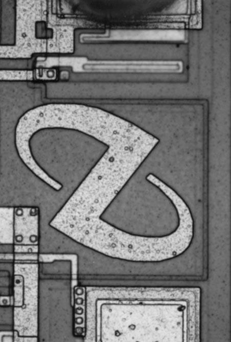
50 PASSIVATION STEP CRACK STEP emitter N+ PASSIVATION CRACK collector N+ PASSIVATION CRACK base P+ ENHANCEMENT DIFFUSION Figure 27. Detailed views of the NPN transistor. Mag. 8000x.


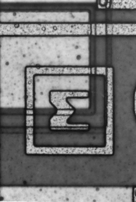
51 N+ BASE Mag. 500x P+ EMITTER P+ COLLECTOR P+ EMITTER N+ BASE CONTACT Mag. 500x P+ COLLECTOR CONTACT Mag. 800x P+ ISO N-EPI P+ EMITTER P+ COLLECTOR N+ BURIED LAYER Figure 28. Optical views of a PNP transistor layout (diode connected).


52 PASSIVATION P+ P EMITTER Mag. 5000x PASSIVATION CRACK IMD P+ Mag. 13,000x Figure 29. SEM section views of a P+ emitter on a PNP device.

.")
53 PROBE MARK Figure 30. Optical views of probe damage and input layout (Pin 2, SS). Mag. 320x.
54 POLY ALUMINUM 1 NITRIDE PASSIVATION PRE-METAL GLASS GLASS PASSIVATION INTERMETAL DIELECTRIC OXIDE OVER P+ ALUMINUM 2,,,,,,,,,, P-WELL N+ S/D N-EPI OXIDE OVER N+ P+ ISO P SUBSTRATE N+ BURIED LAYER N+ EMITTER P+ BASE Orange = Nitride, Blue = Metal, Yellow = Oxide, Green = Poly, Red = Diffusion, and Gray = Substrate Figure 31. Color cross section drawing illustrating device structure. P+ N+ COLLECTOR
SGS-Thomson L4990 Controller
 Construction Analysis SGS-Thomson L4990 Controller Report Number: SCA 9710-560 Global Semiconductor Industry the Serving Since 1964 17350 N. Hartford Drive Scottsdale, AZ 85255 Phone: 602-515-9780 Fax:
Rockwell R RF to IF Down Converter
 Construction Analysis Rockwell R6732-13 RF to IF Down Converter Report Number: SCA 9709-552 Global Semiconductor Industry the Serving Since 1964 17350 N. Hartford Drive Scottsdale, AZ 85255 Phone: 602-515-9780
Maximum MAX662 12V DC-DC Converter
 Construction Analysis Maximum MAX662 12V DC-DC Converter Report Number: SCA 9512-445 Global Semiconductor Industry the Serving Since 1964 17350 N. Hartford Drive Scottsdale, AZ 85255 Phone: 602-515-9780
SGS-Thomson M28C K EEPROM
 Construction Analysis SGS-Thomson M28C64-121 64K EEPROM Report Number: SCA 9710-559 Global Semiconductor Industry the Serving Since 1964 17350 N. Hartford Drive Scottsdale, AZ 85255 Phone: 602-515-9780
Motorola MPA1016FN FPGA
 Construction Analysis Motorola MPA1016FN FPGA Report Number: SCA 9711-561 Global Semiconductor Industry the Serving Since 1964 17350 N. Hartford Drive Scottsdale, AZ 85255 Phone: 602-515-9780 Fax: 602-515-9781
Mosel Vitelic MS62256CLL-70PC 256Kbit SRAM
 Construction Analysis Mosel Vitelic MS62256CLL-70PC 256Kbit SRAM Report Number: SCA 9703-499 Global Semiconductor Industry the Serving Since 1964 17350 N. Hartford Drive Scottsdale, AZ 85255 Phone: 602-515-9780
Oki M A-60J 16Mbit DRAM (EDO)
") Construction Analysis Oki M5117805A-60J 16Mbit DRAM (EDO) Report Number: SCA 9707-545 Global Semiconductor Industry the Serving Since 1964 17350 N. Hartford Drive Scottsdale, AZ 85255 Phone: 602-515-9780
Construction Analysis Oki M5117805A-60J 16Mbit DRAM (EDO) Report Number: SCA 9707-545 Global Semiconductor Industry the Serving Since 1964 17350 N. Hartford Drive Scottsdale, AZ 85255 Phone: 602-515-9780
NEC 79VR5000 RISC Microprocessor
 Construction Analysis NEC 79VR5000 RISC Microprocessor Report Number: SCA 9711-567 Global Semiconductor Industry the Serving Since 1964 17350 N. Hartford Drive Scottsdale, AZ 85255 Phone: 602-515-9780
Micron Semiconductor MT5C64K16A1DJ 64K x 16 SRAM
 Construction Analysis Micron Semiconductor MT5C64K16A1DJ 64K x 16 SRAM Report Number: SCA 9412-394 Global Semiconductor Industry the Serving Since 1964 17350 N. Hartford Drive Scottsdale, AZ 85255 Phone:
VTC VM365830VSJ Pre-Amp
 Construction Analysis VTC VM365830VSJ Pre-Amp Report Number: SCA 9708-549 Global Semiconductor Industry the Serving Since 1964 17350 N. Hartford Drive Scottsdale, AZ 85255 Phone: 602-515-9780 Fax: 602-515-9781
Motorola MC68360EM25VC Communication Controller
 Construction Analysis EM25VC Communication Controller Report Number: SCA 9711-562 Global Semiconductor Industry the Serving Since 1964 17350 N. Hartford Drive Scottsdale, AZ 85255 Phone: 602-515-9780 Fax:
DEC SA-110S StrongARM 32-Bit Microprocessor
 Construction Analysis DEC SA-110S StrongARM 32-Bit Microprocessor Report Number: SCA 9704-535 Global Semiconductor Industry the Serving Since 1964 15022 N. 75th Street Scottsdale, AZ 85260-2476 Phone:
NKK NR4645LQF Bit RISC Microprocessor
 Construction Analysis NKK NR4645LQF-133 64-Bit RISC Microprocessor Report Number: SCA 9707-547 Global Semiconductor Industry the Serving Since 1964 17350 N. Hartford Drive Scottsdale, AZ 85255 Phone: 602-515-9870
Micron Semiconductor MT4LC16M4H9 64Mbit DRAM
 Construction Analysis Micron Semiconductor MT4LC16M4H9 64Mbit DRAM Report Number: SCA 9705-539 Global Semiconductor Industry the Serving Since 1964 15022 N. 75th Street Scottsdale, AZ 85260-2476 Phone:
Hitachi A 64Mbit (8Mb x 8) Dynamic RAM
 Dynamic RAM") Construction Analysis Hitachi 5165805A 64Mbit (8Mb x 8) Dynamic RAM Report Number: SCA 9712-565 Global Semiconductor Industry the Serving Since 1964 17350 N. Hartford Drive Scottsdale, AZ 85255 Phone:
Construction Analysis Hitachi 5165805A 64Mbit (8Mb x 8) Dynamic RAM Report Number: SCA 9712-565 Global Semiconductor Industry the Serving Since 1964 17350 N. Hartford Drive Scottsdale, AZ 85255 Phone:
Dallas Semicoductor DS80C320 Microcontroller
 Construction Analysis Dallas Semicoductor DS80C320 Microcontroller Report Number: SCA 9702-525 Global Semiconductor Industry the Serving Since 1964 15022 N. 75th Street Scottsdale, AZ 85260-2476 Phone:
UMC UM F-7 2M-Bit SRAM
 Construction Analysis UMC UM 613264F-7 2M-Bit SRAM Report Number: SCA 9609-511 Global Semiconductor Industry the Serving Since 1964 15022 N. 75th Street Scottsdale, AZ 85260-2476 Phone: 602-998-9780 Fax:
Analog Devices ADSP KS-160 SHARC Digital Signal Processor
 Construction Analysis Analog Devices ADSP-21062-KS-160 SHARC Digital Signal Processor Report Number: SCA 9712-575 Global Semiconductor Industry the Serving Since 1964 17350 N. Hartford Drive Scottsdale,
Lattice isplsi1032e CPLD
 Construction Analysis Lattice isplsi1032e CPLD Report Number: SCA 9612-522 Global Semiconductor Industry the Serving Since 1964 15022 N. 75th Street Scottsdale, AZ 85260-2476 Phone: 602-998-9780 Fax: 602-948-1925
SGS-Thomson M17C1001 1Mb UVEPROM
 Construction Analysis SGS-Thomson M17C1001 1Mb UVEPROM Report Number: SCA 9612-518 Global Semiconductor Industry the Serving Since 1964 15022 N. 75th Street Scottsdale, AZ 85260-2476 Phone: 602-998-9780
Altera EPM7128SQC EPLD
 Construction Analysis Altera EPM7128SQC160-15 EPLD Report Number: SCA 9712-569 Global Semiconductor Industry the Serving Since 1964 17350 N. Hartford Drive Scottsdale, AZ 85255 Phone: 602-515-9780 Fax:
Lattice 3256A-90LM PLD
 Construction Analysis PLD Report Number: SCA 9705-538 Global Semiconductor Industry the Serving Since 1964 17350 N. Hartford Drive Scottsdale, AZ 85255 Phone: 602-515-9780 Fax: 602-515-9781 e-mail: ice@ice-corp.com
Motorola PC603R Microprocessor
 Construction Analysis Motorola PC603R Microprocessor Report Number: SCA 9709-551 Global Semiconductor Industry the Serving Since 1964 17350 N. Hartford Drive Scottsdale, AZ 85255 Phone: 602-515-9780 Fax:
Xilinx XC4036XL-1C FPGA
 Construction Analysis Xilinx XC4036XL-1C FPGA Report Number: SCA 9709-553 Global Semiconductor Industry the Serving Since 1964 17350 N. Hartford Drive Scottsdale, AZ 85255 Phone: 602-515-9780 Fax: 602-515-9781
Intel Pentium Processor W/MMX
 Construction Analysis Intel Pentium Processor W/MMX Report Number: SCA 9706-540 Global Semiconductor Industry the Serving Since 1964 15022 N. 75th Street Scottsdale, AZ 85260-2476 Phone: 602-998-9780 Fax:
Xilinx XC4036EX FPGA
 Construction Analysis Xilinx XC4036EX FPGA Report Number: SCA 9706-544 Global Semiconductor Industry the Serving Since 1964 15022 N. 75th Street Scottsdale, AZ 85260-2476 Phone: 602-998-9780 Fax: 602-948-1925
Integrated Circuit Engineering Corporation. DRAMs
 DRAMs As generally known, the focus of technology in this product category continues to be complex vertical polysilicon structures to reduce cell area. This not only pushes the limits of deposition and
Integrated Circuit Engineering Corporation EPROM
 EPROM There was lots of discussion and many technical papers covering the promises of EPROM (typically Flash) at the IEDM conference last December, but here as in the other memory areas, not much in the
Lecture 030 Integrated Circuit Technology - I (5/8/03) Page 030-1
 Page 030-1") Lecture 030 Integrated Circuit Technology - I (5/8/03) Page 030-1 LECTURE 030 INTEGRATED CIRCUIT TECHNOLOGY - I (References [7,8]) Objective The objective of this presentation is: 1.) Illustrate integrated
Lecture 030 Integrated Circuit Technology - I (5/8/03) Page 030-1 LECTURE 030 INTEGRATED CIRCUIT TECHNOLOGY - I (References [7,8]) Objective The objective of this presentation is: 1.) Illustrate integrated
Renesas M5M40R326 32Mbit DRAM Memory Structural Analysis
 August 13, 2004 Renesas M5M40R326 32Mbit DRAM Memory Structural Analysis For questions, comments, or more information about this report, or for any additional technical needs concerning semiconductor technology,
Lecture 200 BiCMOS Technology (12/12/01) Page 200-1
 Page 200-1") Lecture 200 BiCMOS Technology (12/12/01) Page 200-1 LECTURE 200 BICMOS TECHNOLOGY (READING: Text-Sec. 2.11) INTRODUCTION Objective Illustrate BiCMOS technology Outline Introduction Physical process illustration
Lecture 200 BiCMOS Technology (12/12/01) Page 200-1 LECTURE 200 BICMOS TECHNOLOGY (READING: Text-Sec. 2.11) INTRODUCTION Objective Illustrate BiCMOS technology Outline Introduction Physical process illustration
9/4/2008 GMU, ECE 680 Physical VLSI Design
 ECE680: Physical VLSI Design Chapter II CMOS Manufacturing Process 1 Dual-Well Trench-Isolated CMOS Process gate-oxide TiSi 2 AlCu Tungsten SiO 2 p-well poly n-well SiO 2 n+ p-epi p+ p+ 2 Schematic Layout
Chapter 2 Manufacturing Process
 Digital Integrated Circuits A Design Perspective Chapter 2 Manufacturing Process 1 CMOS Process 2 CMOS Process (n-well) Both NMOS and PMOS must be built in the same silicon material. PMOS in n-well NMOS
Packaging and Ball Bonding Gold wire makes contact from bonding pads on chip to package Gold wire is formed into ball to make contact Uses an
 Packaging and Ball Bonding Gold wire makes contact from bonding pads on chip to package Gold wire is formed into ball to make contact Uses an ultrasonic process & heat Process called "Ball Bonding" Wedge
EE 434 Lecture 9. IC Fabrication Technology
 EE 434 Lecture 9 IC Fabrication Technology Quiz 7 The layout of a film resistor with electrodes A and B is shown. If the sheet resistance of the film is 40 /, determine the resistance between nodes A and
CMOS Technology. Flow varies with process types & company. Start with substrate selection. N-Well CMOS Twin-Well CMOS STI
 CMOS Technology Flow varies with process types & company N-Well CMOS Twin-Well CMOS STI Start with substrate selection Type: n or p Doping level, resistivity Orientation, 100, or 101, etc Other parameters
EE 330 Lecture 9. IC Fabrication Technology Part 2
 EE 330 Lecture 9 IC Fabrication Technology Part 2 Quiz 8 A 2m silicon crystal is cut into wafers using a wire saw. If the wire diameter is 220um and the wafer thickness is 350um, how many wafers will this
EE 330 Lecture 9. IC Fabrication Technology Part II. -Oxidation -Epitaxy -Polysilicon -Planarization -Resistance and Capacitance in Interconnects
 EE 330 Lecture 9 IC Fabrication Technology Part II -Oxidation -Epitaxy -Polysilicon -Planarization -Resistance and Capacitance in Interconnects Review from Last Time Etching Dry etch (anisotropic) SiO
Manufacturing Process
 CMOS Manufacturing Process CMOS Process 1 A Modern CMOS Process gate-oxide TiSi AlCu Tungsten SiO n+ p-well p-epi poly n-well p+ SiO p+ Dual-Well Trench-Isolated CMOS Process Circuit Under Design V DD
CMOS Manufacturing Process
 CMOS Manufacturing Process CMOS Process A Modern CMOS Process gate-oxide TiSi 2 AlCu Tungsten SiO 2 n+ p-well p-epi poly n-well p+ SiO 2 p+ Dual-Well Trench-Isolated CMOS Process Circuit Under Design V
Manufacturing Process
 Manufacturing Process 1 CMOS Process 2 A Modern CMOS Process gate-oxide TiSi 2 AlCu Tungsten SiO 2 n+ p-well p-epi poly n-well p+ SiO 2 p+ Dual-Well Trench-Isolated CMOS Process 3 Single-crystal ingot
EE 560 FABRICATION OF MOS CIRCUITS. Kenneth R. Laker, University of Pennsylvania
 1 EE 560 FABRICATION OF MOS CIRCUITS 2 CMOS CHIP MANUFACTRING STEPS Substrate Wafer Wafer Fabrication (diffusion, oxidation, photomasking, ion implantation, thin film deposition, etc.) Finished Wafer Wafer
EE 330 Lecture 9. IC Fabrication Technology Part II. -Oxidation -Epitaxy -Polysilicon -Planarization -Resistance and Capacitance in Interconnects
 EE 330 Lecture 9 IC Fabrication Technology Part II -Oxidation -Epitaxy -Polysilicon -Planarization -Resistance and Capacitance in Interconnects Review from Last Time IC Fabrication Technology Crystal Preparation
We are moving to 155 Donner Lab From Thursday, Feb 2 We will be able to accommodate everyone!
 -Spring 006 Digital Integrated Circuits Lecture 4 CMOS Manufacturing Process Design Rules EECS141 1 Good News! We are moving to 155 Donner Lab From Thursday, Feb We will be able to accommodate everyone!
Manufacturing Process
 Digital Integrated Circuits A Design Perspective Jan M. Rabaey Anantha Chandrakasan Borivoje Nikolic Manufacturing Process July 30, 2002 1 CMOS Process 2 A Modern CMOS Process gate-oxide TiSi 2 AlCu Tungsten
Microelectronics. Integrated circuits. Introduction to the IC technology M.Rencz 11 September, Expected decrease in line width
 Microelectronics Introduction to the IC technology M.Rencz 11 September, 2002 9/16/02 1/37 Integrated circuits Development is controlled by the roadmaps. Self-fulfilling predictions for the tendencies
ECE 659. Jan M. Rabaey Anantha Chandrakasan Borivoje Nikolic. July 30, Digital EE141 Integrated Circuits 2nd Manufacturing.
 Digital Integrated Circuits A Design Perspective Jan M. Rabaey Anantha Chandrakasan Borivoje Nikolic Manufacturing Process July 0, 00 1 CMOS Process 1 A Modern CMOS Process gate-oxide TiSi AlCu Tungsten
Department of Electrical Engineering. Jungli, Taiwan
 Chapter 3 Fabrication of CMOS Integrated Circuits Jin-Fu Li Department of Electrical Engineering National Central University Jungli, Taiwan Background Outline The CMOS Process Flow Design Rules Latchup
Process Integration. NMOS Generic NMOS Process Flow. CMOS - The MOSIS Process Flow
 Process Integration Self-aligned Techniques LOCOS- self-aligned channel stop Self-aligned Source/Drain Lightly Doped Drain (LDD) Self-aligned silicide (SALICIDE) Self-aligned oxide gap MEMS Release Techniques
FABRICATION of MOSFETs
 FABRICATION of MOSFETs CMOS fabrication sequence -p-type silicon substrate wafer -creation of n-well regions for pmos transistors, -impurity implantation into the substrate. -thick oxide is grown in the
Chapter 4 : ULSI Process Integration (0.18 m CMOS Process)
") Chapter : ULSI Process Integration (0.8 m CMOS Process) Reference. Semiconductor Manufacturing Technology : Michael Quirk and Julian Serda (00). - (00). Semiconductor Physics and Devices- Basic Principles(/e)
Chapter : ULSI Process Integration (0.8 m CMOS Process) Reference. Semiconductor Manufacturing Technology : Michael Quirk and Julian Serda (00). - (00). Semiconductor Physics and Devices- Basic Principles(/e)
HOMEWORK 4 and 5. March 15, Homework is due on Monday March 30, 2009 in Class. Answer the following questions from the Course Textbook:
 HOMEWORK 4 and 5 March 15, 2009 Homework is due on Monday March 30, 2009 in Class. Chapter 7 Answer the following questions from the Course Textbook: 7.2, 7.3, 7.4, 7.5, 7.6*, 7.7, 7.9*, 7.10*, 7.16, 7.17*,
Silicon Epitaxial CVD Want to create very sharp PN boundary grow one type layer on other in single crystal form High dopant layers on low dopant
 Silicon Epitaxial CVD Want to create very sharp PN boundary grow one type layer on other in single crystal form High dopant layers on low dopant substrate Creates latch up protection for CMOS Buried Epi
Fairchild Semiconductor Application Note June 1983 Revised March 2003
 Fairchild Semiconductor Application Note June 1983 Revised March 2003 High-Speed CMOS (MM74HC) Processing The MM74HC logic family achieves its high speed by utilizing microcmos Technology. This is a 3.5
VLSI Technology Dr. Nandita Dasgupta Department of Electrical Engineering Indian Institute of Technology, Madras
 VLSI Technology Dr. Nandita Dasgupta Department of Electrical Engineering Indian Institute of Technology, Madras Lecture - 32 IC BJT - From junction isolation to LOCOS So, by now, we have completed all
Process Integration. MEMS Release Techniques Sacrificial Layer Removal Substrate Undercut
 Process Integration Self-aligned Techniques LOCOS- self-aligned channel stop Self-aligned Source/Drain Lightly Doped Drain (LDD) Self-aligned silicide (SALICIDE) Self-aligned oxide gap MEMS Release Techniques
VLSI Technology Dr. Nandita Dasgupta Department of Electrical Engineering Indian Institute of Technology, Madras
 VLSI Technology Dr. Nandita Dasgupta Department of Electrical Engineering Indian Institute of Technology, Madras Lecture - 36 MOSFET I Metal gate vs self-aligned poly gate So far, we have discussed about
VLSI Technology Dr. Nandita Dasgupta Department of Electrical Engineering Indian Institute of Technology, Madras
 VLSI Technology Dr. Nandita Dasgupta Department of Electrical Engineering Indian Institute of Technology, Madras Lecture - 33 Problems in LOCOS + Trench Isolation and Selective Epitaxy So, we are discussing
ECE520 VLSI Design. Lecture 7: CMOS Manufacturing Process. Payman Zarkesh-Ha
 ECE520 VLSI Design Lecture 7: CMOS Manufacturing Process Payman Zarkesh-Ha Office: ECE Bldg. 230B Office hours: Wednesday 2:00-3:00PM or by appointment E-mail: pzarkesh@unm.edu Slide: 1 Review of Last
Mark T. Bohr Intel Senior Fellow, Technology and Manufacturing Group Director, Process Architecture and Integration INTEL CORPORATION
 Mark T. Bohr Intel Senior Fellow, Technology and Manufacturing Group Director, Process Architecture and Integration INTEL CORPORATION Patents» 6762464, N-P butting connections on SOI substrates, 7/13/2004.»
CMOS Processing Technology
 CHAPTER 2 CMOS Processing Technology Outline 2 1. CMOS Technologies 2. Layout Design Rules 3. CMOS Process Enhancements 4. Technology-related CAD Issues 5. Manufacturing Issues CMOS Technologies 3 n-well
CMOS Processing Technology
 CHAPTER 2 CMOS Processing Technology Outline 2 1. CMOS Technologies 2. Layout Design Rules 3. CMOS Process Enhancements 4. Technology-related CAD Issues 5. Manufacturing Issues CMOS Technologies 3 n-well
Silicon Epitaxial CVD Want to create very sharp PN boundary grow one type layer on other in single crystal form High dopant layers on low dopant
 Silicon Epitaxial CVD Want to create very sharp PN boundary grow one type layer on other in single crystal form High dopant layers on low dopant substrate Creates latch up protection for CMOS Buried Epi
CHAPTER - 4 CMOS PROCESSING TECHNOLOGY
 CHAPTER - 4 CMOS PROCESSING TECHNOLOGY Samir kamal Spring 2018 4.1 CHAPTER OBJECTIVES 1. Introduce the CMOS designer to the technology that is responsible for the semiconductor devices that might be designed
Isolation Technology. Dr. Lynn Fuller
 ROCHESTER INSTITUTE OF TECHNOLOGY MICROELECTRONIC ENGINEERING Isolation Technology Dr. Lynn Fuller Motorola Professor 82 Lomb Memorial Drive Rochester, NY 14623-5604 Tel (585) 475-2035 Fax (585) 475-5041
CMOS Manufacturing process. Design rule set
 CMOS Manufacturing process Circuit design Set of optical masks Fabrication process Circuit designer Design rule set Process engineer All material: Chap. 2 of J. Rabaey, A. Chandrakasan, B. Nikolic, Digital
PROCESS FLOW AN INSIGHT INTO CMOS FABRICATION PROCESS
 Contents: VI Sem ECE 06EC63: Analog and Mixed Mode VLSI Design PROCESS FLOW AN INSIGHT INTO CMOS FABRICATION PROCESS 1. Introduction 2. CMOS Fabrication 3. Simplified View of Fabrication Process 3.1 Alternative
SCMOS Layout Rules - Well
 SCMOS Layout s - Well 1.1 Minimum width 12 3.6 1.2 Minimum spacing between wells at different potential 18 5.4 1.3 Minimum spacing between wells at same potential 6 1.8 1.4 Minimum spacing between wells
EE 330 Lecture 8. IC Fabrication Technology Part II. - Oxidation - Epitaxy - Polysilicon - Interconnects
 EE 330 Lecture 8 IC Fabrication Technology Part II - Oxidation - Epitaxy - Polysilicon - Interconnects Review from Last Time MOS Transistor Bulk Source Gate Drain p-channel MOSFET Lightly-doped n-type
ECE321 Electronics I
 ECE321 Electronics I Lecture 19: CMOS Fabrication Payman Zarkesh-Ha Office: ECE Bldg. 230B Office hours: Tuesday 2:00-3:00PM or by appointment E-mail: payman@ece.unm.edu Slide: 1 Miller Effect Interconnect
CMOS FABRICATION. n WELL PROCESS
 CMOS FABRICATION n WELL PROCESS Step 1: Si Substrate Start with p- type substrate p substrate Step 2: Oxidation Exposing to high-purity oxygen and hydrogen at approx. 1000 o C in oxidation furnace SiO
Fabrication and Layout
 ECEN454 Digital Integrated Circuit Design Fabrication and Layout ECEN 454 3.1 A Glimpse at MOS Device Polysilicon Aluminum ECEN 475 4.2 1 Material Classification Insulators Glass, diamond, silicon oxide
ASIM-X MEMS-Specific Design Rules
 ASIM-X MEMS-Specific Design Rules Version 2 Revised April 5, 2006. This is a beta version, subject to change. Revised by G. K. Fedder, Carnegie Mellon University. 1 Process Overview ASIM-X, an acronym
Microelectronics Devices
 Microelectronics Devices Yao-Joe Yang 1 Outline Basic semiconductor physics Semiconductor devices Resistors Capacitors P-N diodes BJT/MOSFET 2 Type of Solid Materials Solid materials may be classified
Silicon Wafer Processing PAKAGING AND TEST
 Silicon Wafer Processing PAKAGING AND TEST Parametrical test using test structures regularly distributed in the wafer Wafer die test marking defective dies dies separation die fixing (not marked as defective)
UT Austin, ECE Department VLSI Design 2. CMOS Fabrication, Layout Rules
 2. CMOS Fabrication, Layout, Design Rules Last module: Introduction to the course How a transistor works CMOS transistors This module: CMOS Fabrication Design Rules CMOS Fabrication CMOS transistors are
Lecture 1A: Manufacturing& Layout
 Introduction to CMOS VLSI Design Lecture 1A: Manufacturing& Layout David Harris Harvey Mudd College Spring 2004 Steven Levitan Fall 2008 1 The Manufacturing Process For a great tour through the IC manufacturing
VLSI Systems and Computer Architecture Lab
 ΚΥΚΛΩΜΑΤΑ VLSI Πανεπιστήμιο Ιωαννίνων CMOS Technology Τμήμα Μηχανικών Η/Υ και Πληροφορικής 1 From the book: An Introduction ti to VLSI Process By: W. Maly ΚΥΚΛΩΜΑΤΑ VLSI Διάρθρωση 1. N well CMOS 2. Active
Chapter 3 CMOS processing technology
 Chapter 3 CMOS processing technology (How to make a CMOS?) Si + impurity acceptors(p-type) donors (n-type) p-type + n-type => pn junction (I-V) 3.1.1 (Wafer) Wafer = A disk of silicon (0.25 mm - 1 mm thick),
Is Now Part of To learn more about ON Semiconductor, please visit our website at
 Is Now Part of To learn more about ON Semiconductor, please visit our website at www.onsemi.com ON Semiconductor and the ON Semiconductor logo are trademarks of Semiconductor Components Industries, LLC
TOWARD MEMS!Instructor: Riadh W. Y. Habash
 TOWARD MEMS!Instructor: Riadh W. Y. Habash Students are presented with aspects of general production and manufacturing of integrated circuit (IC) products to enable them to better liaise with and participate
INTEGRATED-CIRCUIT TECHNOLOGY
 INTEGRATED-CIRCUIT TECHNOLOGY 0. Silicon crystal growth and wafer preparation 1. Processing Steps 1.1. Photolitography 1.2. Oxidation 1.3. Layer Deposition 1.4. Etching 1.5. Diffusion 1.6 Backend: assembly,
A LOW SERIES RESISTANCE, HIGH DENSITY, TRENCH CAPACITOR FOR HIGH-FREQUENCY APPLICATIONS
 A LOW SERIES RESISTANCE, HIGH DENSITY, TRENCH CAPACITOR FOR HIGH-FREQUENCY APPLICATIONS Gordon Grivna, Sudhama Shastri, Yujing Wu, & Will Cai Sept, 2008 www.onsemi.com Presentation Outline 1. Introduction
Cost of Integrated Circuits
 Cost of IC Design 1 Cost of Integrated Circuits NRE (Non-Recurrent Engineering) costs fixed design time and effort, mask generation independent of sales volume / number of products one-time cost factor
1 Thin-film applications to microelectronic technology
 1 Thin-film applications to microelectronic technology 1.1 Introduction Layered thin-film structures are used in microelectronic, opto-electronic, flat panel display, and electronic packaging technologies.
EE 143 CMOS Process Flow
 EE 143 CMOS rocess Flow CT 84 D D G Sub G Sub S S G D S G D S + + + + - MOS Substrate Well - MOS Substrate EE 143 CMOS rocess Flow CT 85 hotoresist Si 3 4 SiO 2 Substrate selection: moderately high resistivity,
MOS Front-End. Field effect transistor
 MOS Front-End Back-end Transistor Contact Front-end p-well STI n-well Front-end-of-line includes substrate, isolation, wells, transistor, silicide Field effect transistor MOSFET: Metal-Oxide-Semiconductor
VLSI INTRODUCTION P.VIDYA SAGAR ( ASSOCIATE PROFESSOR) Department of Electronics and Communication Engineering, VBIT
 Department of Electronics and Communication Engineering, VBIT") VLSI INTRODUCTION P.VIDYA SAGAR ( ASSOCIATE PROFESSOR) contents UNIT I INTRODUCTION: Introduction to IC Technology MOS, PMOS, NMOS, CMOS & BiCMOS technologies. BASIC ELECTRICAL PROPERTIES : Basic Electrical
VLSI INTRODUCTION P.VIDYA SAGAR ( ASSOCIATE PROFESSOR) contents UNIT I INTRODUCTION: Introduction to IC Technology MOS, PMOS, NMOS, CMOS & BiCMOS technologies. BASIC ELECTRICAL PROPERTIES : Basic Electrical
This Appendix discusses the main IC fabrication processes.
 IC Fabrication B B.1 Introduction This Appendix discusses the main IC fabrication processes. B.2 NMOS fabrication NMOS transistors are formed in a p-type substrate. The NMOS fabrication process requires
10 Manor Parkway, Suite C Salem, New Hampshire
 Micro-Precision Technologies (MPT) is an independent manufacturer of hybrid integrated circuits, multichip modules, and high-precision thick film substrates for the military, medical, avionics, optoelectronics,
Chapter 2 Problems. The CMOS technology we need to realize is shown below, from Figure 1-34 in the text. S P + N P + N WELL P +
 Chapter 2 roblems 2.1 Sketch a process flow that would result in the structure shown in Figure 1-34 by drawing a series of drawings similar to those in this chapter. You only need to describe the flow
Enhancement Mode GaN FETs and ICs Visual Characterization Guide
 Enhancement Mode GaN FETs and ICs Visual Characterization Guide EFFICIENT POWER CONVERSION Alana Nakata, Vice President, Product Engineering, Efficient Power Conversion Corporation A detailed description
Oxidation SMT Yau - 1
 Oxidation Yau - 1 Objectives After studying the material in this chapter, you will be able to: 1. Describe an oxide film for semiconductor manufacturing, including its atomic structure, how it is used
EE CMOS TECHNOLOGY- Chapter 2 in the Text
 1 EE 212 FALL 1999-00 CMOS TECHOLOGY- Chapter 2 in the Text In this set of notes we will describe a modern CMOS process flow. In the simplest CMOS technologies, we need to realize simply MOS and MOS transistors
Introduction to CMOS VLSI Design. Layout, Fabrication, and Elementary Logic Design
 Introduction to CMOS VLSI Design Layout, Fabrication, and Elementary Logic Design CMOS Fabrication CMOS transistors are fabricated on silicon wafer Lithography process similar to printing press On each
VLSI Digital Systems Design
 VLSI Digital Systems Design CMOS Processing cmpe222_03process_ppt.ppt 1 Si Purification Chemical purification of Si Zone refined Induction furnace Si ingot melted in localized zone Molten zone moved from
IC Fabrication Technology Part III Devices in Semiconductor Processes
 EE 330 Lecture 10 IC Fabrication Technology Part III Metalization and Interconnects Parasitic Capacitances Back-end Processes Devices in Semiconductor Processes Resistors Diodes Review from Last Lecture
Fabrication and Layout
 Fabrication and Layout Kenneth Yun UC San Diego Adapted from EE271 notes, Stanford University Overview Semiconductor properties How chips are made Design rules for layout Reading Fabrication: W&E 3.1,
VLSI Technology. By: Ajay Kumar Gautam
 By: Ajay Kumar Gautam Introduction to VLSI Technology, Crystal Growth, Oxidation, Epitaxial Process, Diffusion Process, Ion Implantation, Lithography, Etching, Metallization, VLSI Process Integration,
CX Thin Fil s. Resistors Attenuators Thin-Film Products Thin-Film Services. ISO 9001:2008 RoHS/REACH Compliant ITAR Compliant
 CX Thin Fil s Resistors Attenuators Thin-Film Products Thin-Film Services www.cxthinfilms.com ISO 9001:2008 RoHS/REACH Compliant ITAR Compliant www.cxthinfilms.com sales@cxthinfilms.com +1 (401) 461-5500