The Morphology Evolution and Voiding of Solder Joints on QFN Central Pads with a Ni/Au Finish
|
|
|
- Brendan Tyler
- 6 years ago
- Views:
Transcription
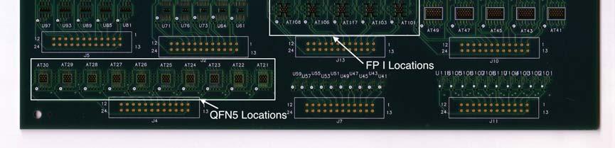
1 The Morphology Evolution and Voiding of Solder Joints on QFN Central Pads with a Ni/Au Finish Julie Silk 1, Jianbiao Pan 2, Mike Powers 1 1 Agilent Technologies, 1400 Fountaingrove Parkway, Santa Rosa, CA California Polytechnic State University, San Luis Obispo, CA Abstract In this paper, we report on a comprehensive study regarding the morphology evolution and voiding of SnAgCu solder joints on the central pad of two different packages QFN and an Agilent package called TOPS on PCBs with a Ni/Au surface finish. Samples were isothermally aged at the equivalent of 0, 2, 7 and 14 years service life. Representative solder joints were cross-sectioned and analyzed using scanning electron microscopy (SEM) and energy dispersive X-ray spectroscopy (EDX) in order to investigate the evolution of the solder joint morphology as a function of Au content and isothermal aging. IMC thickness was measured. The effect of Au content on the void percentage was studied as well. The results show that if copper is available to dissolve into the solder joint, the AuSn 4 IMC from the bulk does not migrate to the interface as a result of thermal aging. The IMC thickness grew with aging as expected, however with Cu base metallization the IMC was dominated by Cu 6 Sn 5, and with Ni base metallization on both sides of the joint the IMC was dominated by AuSn 4. Voiding analysis showed that thick Au metallization on thermal pads leads to more voiding and larger standoff height. Introduction The Quad Flat No-lead (QFN) package is increasingly popular due to its small size, easy trace routing, and good thermal and electrical performance [1]. It has a large central underbelly pad, which dissipates heat from the die inside the package through a solder connection to the printed circuit board (PCB). The short standoff distance between the QFN package and the PCB also reduces inductance thus providing excellent electrical performance. An Agilent package called TOPS has features similar to a QFN, being leadless with a large underbelly pad. Although the QFN package and the TOPS packages offer a number of benefits, to the authors knowledge, the evolution of morphology of the solder joint on the central underbelly pad has not been reported. In this paper, we report on a comprehensive study regarding the effect of Au content on the morphology of SnAgCu solder joints on the underbelly pad, assembled on PCBs with a Ni/Au surface finish. Samples were isothermally aged at the equivalent of 0, 2, 7 and 14 years service life. Representative solder joints were cross-sectioned and analyzed using scanning electron microscopy (SEM) and energy dispersive X-ray spectroscopy (EDX) in order to investigate the evolution of the solder joint morphology as a function of Au content and isothermal aging. Another issue with these leadless packages with a large underbelly pad is that excessive voiding often occurs in the solder joint on the underbelly pad. If the void area is large, thermal performance will be reduced. There are a few application notes that provide guidelines for pad pattern design, stencil design, reflow profile, and others [2-6]. To the authors knowledge, no paper has been published on the effect of Au content on the voiding. In this paper, the effect of Au content on voiding in the underbelly solder joint is reported. Experiment Component, Test Vehicle, and Assembly Process The test vehicle is shown in Figure 1. The board finish is electrolytic Au over Ni. There are two different Au thicknesses: a flash Au finish with 0.08 ~ 0.38 µm Au over 5 µm Ni and a thick Au finish with 2 ~ 2.54 µm Au over 5 µm Ni. Two types of leadless packages, QFNs and TOPS, were assembled on the test vehicle. Figure 2 shows these packages. The QFNs were two different sizes: QFN5 is 5 mm x 5 mm and QFN6 is 6 mm x 6 mm. The size of the TOPS package is 10 mm x 10 mm. The pad finish on the QFN5 and QFN6 is matte Sn over Cu and that on the TOPS is electrolytic Au over Ni. The assembly process was done using a standard surface mount assembly line in a realistic production environment. The solder paste used is Sn3.0Ag0.5Cu (SAC305) Type 3 with no-clean flux and metal content of 88% by weight. The stencil used is electroformed Nickel, laser cut with a foil thickness of 0.1 mm (4 mils). The solder paste coverage of the central pad for QFN5 and QFN6 is 43% and that for TOPS is 56%. Since the volume of solder paste on the central pad was not measured, the nominal solder paste volume is calculated based on the stencil aperture size and the coverage. The calculated nominal Au content of solder joint on the central pad for QFN5, QFN6, and TOPS package is shown in Table 1. For details about the reflow profile and Au content calculation, please refer to papers published by the authors [7-9].


2 The assembled PCBs were randomly divided into three groups. The boards in Group 1 were not subjected to thermal aging. The boards in Group 2 were subjected to isothermal aging at 125 C for 30 days. The boards in Group 3 were subjected to isothermal aging at 125 C for 56 days. The three thermal aging times represent 0, 7.8 and 14.6 years of service when the device is operated at 60 C. Activation energy of 0.8 ev is used. One flash Au board and one thick Au board from each group were randomly selected for cross-sectioning and SEM/EDX analysis. An additional thick Au board was aged at 125 C for 209 hours, or 2.25 years of service when the device is operated at 60 C. Aging at 125 C for 209 hours is equivalent to 1000 hours at 100 C. The SEM used in this study was a JEOL JSM-6390 equipped with a Thermo Scientific 6733A EDX. Figure 1. Test Vehicle Figure 2. Packaged QFN Components Table 1. Nominal Au Content in Weight Percentage in Solder Joints on Central Pad Flash Au Thick Au QFN5 or QFN6 1.2% 10.9% TOPS 4.1% 11.2%
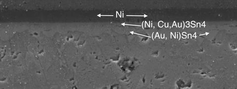
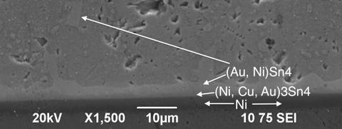
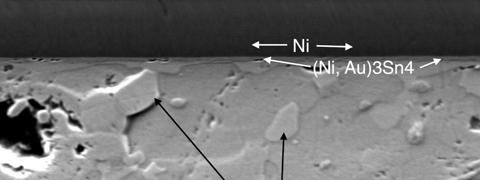
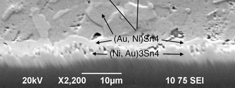
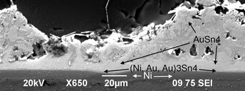
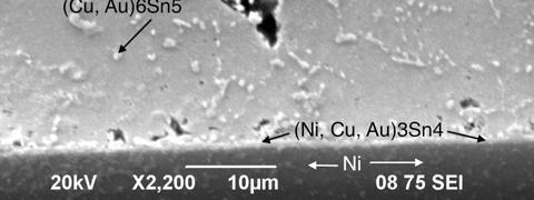
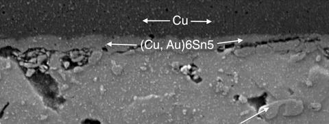
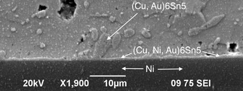
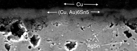
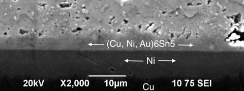
3 Results and Discussion Evolution of Solder Joint Morphology The evolution of the microstructure for both QFN and TOPS solder joints on the underbelly central pad was evaluated. The substrate finish on the QFN package does not have a Ni diffusion barrier and the TOPS package includes a Ni barrier layer in the substrate finish. In both part types, the solder joint microstructure is compared as a function of isothermal aging times and relative Au content in the solder joints. QFN and TOPS on Flash Au Board The SEM micrograph of two as-built solder joints between the central pad of a component and a board with a flash Au finish is shown in Figure 3. The Au content in the QFN solder joint is about 1.2% by weight and the Au content in the TOPS solder joint is about 4.1%. The interfacial intermetallic compound (IMC) on the component side of the QFN solder joint is Cu 6 Sn 5 while that of the TOPS solder joint is (Ni, Cu, Au) 3 Sn 4. This is because the finish of the QFN package does not have a Ni diffusion barrier layer and allows Cu to diffuse into the joint. The TOPS package has a Ni layer. The interfacial IMC on the board side of the QFN joint is (Ni, Cu, Au) 3 Sn 4 or (Cu, Ni, Au) 6 Sn 5 while there are two different IMC layers that can be seen in the board side of the TOPS joint: (Au, Ni)Sn 4 over (Ni, Au) 3 Sn 4 layer. The IMC in the bulk solder of the QFN joint is pebble-like (Cu, Au) 6 Sn 5 while that of the TOPS joint is needle-like AuSn 4. Figure 4 shows the SEM micrograph of two aged solder joints between the central pad of a component and a board with a flash Au finish. The joints were aged at 125ºC for 30 days. For the QFN joint, there is no significant difference in the IMCs and microstructures between the aged sample and the as-built sample except that (Cu, Au) 6 Sn 5 in the bulk solder coalesces to larger sizes. The driving force for this coarsening behavior is the energy reduction associated with a lower surface area to volume ratio. In the TOPS joints, needle-like AuSn 4 IMCs in the bulk solder of the as-built sample changed to stone-like AuSn 4 IMCs after aging. Some AuSn 4 IMCs in the bulk solder migrated with aging to form a continuous (Au, Ni)Sn 4 layer next to the (Ni, Cu, Au) 3 Sn 4 IMC at the interface. In the QFN joints, there is not a continuous layer of detrimental (Au, Ni)Sn 4 IMC in the interface on the flash Au board. After aging at 125ºC for 56 days, one QFN solder joint and one TOPS joint on a flash Au board are shown in the SEM micrographs in Figure 5. The IMCs and microstructures are similar to that of samples aged for 30 days. However, the interfacial IMC thickness increased. QFN and TOPS on Thick Au Board The SEM micrograph of two as-built solder joints between the central pad of a component and a board with a thick Au finish is shown in Figure 6. The Au content in the QFN solder joint is about 10.9% by weight and the Au content in the TOPS solder joint is about 11.2%. The interfacial intermetallic compound (IMC) on the component side of the QFN solder joint is (Cu, Ni, Au) 6 Sn 5 while that of the TOPS solder joint is (Ni, Cu, Au) 3 Sn 4. The IMC in the bulk solder of the QFN joint is pillar-like and/or stone-like AuSn 4, same as that of the TOPS joint. Figures 7 and 8 show the SEM micrographs of solder joints on thick Au boards after aging at 125ºC for 30 days and 56 days, respectively. It is interesting to note that the interfacial IMC of the TOPS joint on the board side is a continuous (Au, Ni)Sn 4 layer next to the (Ni, Cu, Au) 3 Sn 4 IMC while there is no continuous layer of (Au, Ni)Sn 4 at the QFN joint. The result is significant. It is the effect of Cu on AuSn 4 IMC migration. When copper is available, as with the QFN, the AuSn 4 IMCs did not form a continuous interfacial layer. The driving force for the migration of AuSn 4 is a reduction of Gibbs free energy by mixing, consequently establishing an AuSn 4 equilibrium between the bulk and the interface. With the fast diffusion of Cu into the IMC, there is less drive to absorb Ni and thus less migration to the Ni interface. We also noticed that there are large fractures in the solder joint between the central pad of a TOPS and a thick Au board as shown in Figure 9. Such fractures did not occur in solder joints between a TOPS and a flash Au board. Such fractures also did not occur on solder joints between a QFN and a thick Au board. This indicates that high Au content (over 10 wt% Au) has a more severe effect on the reliability of solder joints without Cu (Ni layer on both sides of the joint) than those with the availability of Cu. When copper is available, AuSn 4 IMCs are less likely to migrate to the interface and form a continuous IMC layer, thus improving the reliability.

 QFN b) TOPS Figure 4.")

 QFN b) TOPS Figure 5.")
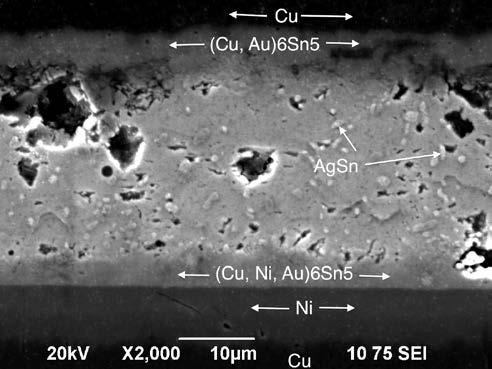
4 a) QFN b) TOPS Figure 3. SEM micrograph of an as-built solder joint between the central pad and a board with flash Au finish. a) QFN b) TOPS Figure 4. SEM micrograph of an aged solder joint between the central pad and a board with flash Au finish. The sample was aged at 125 C for 30 days. a) QFN b) TOPS Figure 5. SEM micrograph of an aged solder joint between the central pad and a board with flash Au finish. The sample was aged at 125 C for 56 days.


 QFN b) TOPS Figure 8.")

5 a) QFN b) TOPS Figure 6. SEM micrograph of an as-built solder joint between the central pad and a board with thick Au finish. a) QFN b) TOPS Figure 7. SEM micrograph of an aged solder joint between the central pad and a board with thick Au finish. The sample was aged at 125 C for 30 days. a) QFN b) TOPS Figure 8. SEM micrograph of an aged solder joint between the central pad and a board with thick Au finish. The sample was aged at 125 C for 56 days.

6 Figure 9. SEM image of the solder joint between the central pad of TOPS component and a thick Au board. Thermal aging time It is useful to know how long is enough for thermal aging. In this study, we compared the microstructure and IMC thickness of solder joints aged at 125ºC for 209 hours vs. for 30 days and 56 days. Figure 10 shows the SEM micrograph of a solder joint between the central pad of a QFN and a thick Au board aged at 125ºC for 209 hours. Comparing with the SEM image of as-built solder joint in Figure 6 a) and the SEM image of aged solder joint in Figure 7 a), it seems the coalescence process of the AuSn 4 IMCs in the bulk solder has completed after aging for 209 hours. There is no significant difference in microstructure between the solder joint aged for 209 hours and the joint aged for 30 days, except that the IMC layer is thicker in the sample aged for 30 days. Figure 11 shows the SEM images of a solder joint between a perimeter lead of a TOPS and a thick board aged at 125ºC for 209 hours, compared with solder joints as-built, aged for 30 days, and aged for 56 days. The same conclusion can be drawn that there is no significant difference in microstructure of the bulk solder joint between the solder joint aged for 209 hours and the joint aged for 30 days or 56 days. However, at the interface, the migration of AuSn 4 to a continuous layer has not yet occurred. This indicates that the 2 year equivalent aging time appears to not be sufficient to see significant migration of the AuSn 4 IMC. Figures 12 and 13 show the changes in mean IMC thickness (four measurements per group) at the component and board interfaces, respectively, as a function of thermal aging time and board finish (thick vs. flash Au) for the QFN platform. For the case of QFN, the IMC thickness and composition at the component and board interfaces can evolve independently, due to the difference in the surface finish stack-up. The evolution of IMC thickness as a function of thermal aging and board finish for the TOPS platform is shown in Figure 14, where the IMC thickness at both interfaces is included in the calculation of the mean thickness (four measurements per group) because composition at the two interfaces is essentially the same for the TOPS platform, owing to the presence of a Ni diffusion barrier at both interfaces. For both platforms, the mean IMC thickness increases with thermal aging time and increases at about the same rate. However, it is interesting to note that for the QFN packages the increase in IMC thickness is higher on the flash Au boards, whereas for the TOPS packages the mean IMC thickness increase is higher for the thick Au boards. Since Cu is readily available in the QFN solder joints, migration of AuSn 4 type IMCs from the bulk to the interfaces during thermal aging is mitigated (i.e. AuSn 4 does not contribute to the increase in IMC thickness) and the IMC growth is dominated by formation of the (Cu, Ni, Au) 6 Sn 5 IMC. In contrast, the presence of a Ni diffusion barrier at both interfaces for the case of the TOPS packages results in migration of (Au, Ni)Sn 4 IMC from the bulk to the interfaces during thermal aging where it contributes to the overall IMC thickness. Since more Au is available in the case of the thick Au boards, it makes sense that the contribution to overall IMC thickness is enhanced.


 Aged at")

7 Figure 10. SEM micrograph of an aged solder joint between the central pad of a QFN and a board with thick Au finish. The sample was aged at 125 C for 209 hours a) As-built b) Aged at 125ºC for 209 hours c) Aged at 125ºC for 30 days d) Aged at 125ºC for 56 days Figure 11. SEM images of solder joints of a TOPS component on a thick Au board


8 Figure 12. IMC thickness for QFN on flash and thick Au boards, component side of interface (error bars are ±1σ) Figure 13. IMC thickness for QFN on flash and thick Au boards, board side of interface (error bars are ±1σ) Figure 14. IMC thickness for TOPS on flash and thick Au boards (error bars are ±1σ)

![A total of 540 images were analyzed including nine QFN5, nine QFN6, and nine TOPS components on 10 flash Au boards and 10 thick Au boards. The analysis was done using the software ImageJ [10].](/docs-images/74/70790177/images/9-1.jpg "By adjusting the contrast and setting a threshold, the software is able to determine all voiding area and calculate the total voiding area. The software also shows the area of each void in the image.")
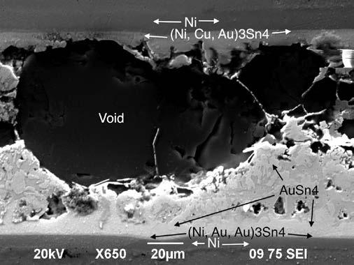
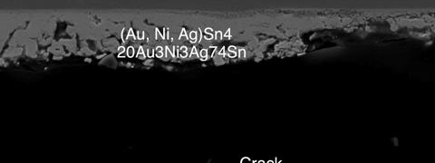
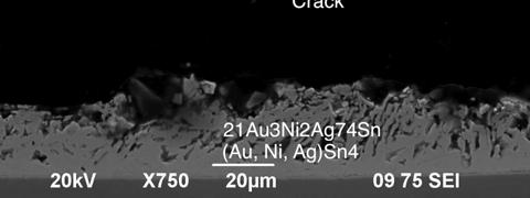
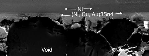
9 Voiding in the central underbelly pad solder joint It is well known that excessive voiding often occurs on the solder joint on the underbelly pad. In this study, a 2D X-ray image was taken on every component on every board after assembly. Figure 15 shows two X-ray images. A total of 540 images were analyzed including nine QFN5, nine QFN6, and nine TOPS components on 10 flash Au boards and 10 thick Au boards. The analysis was done using the software ImageJ [10]. By adjusting the contrast and setting a threshold, the software is able to determine all voiding area and calculate the total voiding area. The software also shows the area of each void in the image. Voiding is characterized using void percentage, which is defined as the ratio of all voiding areas to the central pad area. Figure 16 shows the average void percentage of each component type on the flash Au board and the thick Au board. The number for QFN is an average of 120 components and the number for TOPS is an average of 60 components. It is clear that thick Au metallization on thermal pads leads to more voiding. We also noticed that the majority of voids cover thermal vias in the center of the pad. Note that all thermal vias in the study are un-filled, which was an error in board fabrication. The intended design was to epoxy-fill and plate over these vias, or vippo (via in pad plated over). The SEM image in Figure 17 shows that voids are due to solder loss resulting from solder flowing through thermal vias. Figure 18 shows that interfacial IMCs have been formed on the void area. This indicates that solder wetted the pad on the PCB and on the component, formed IMCs, then solder flowed through thermal vias and voids are created due to the solder loss. The standoff distance of the solder joint on the central pad was measured and reported in Table 2. Note that the stencil thickness is 100 µm (4 mils), and the solder paste coverage of the central pad for QFN5 and QFN6 is 43% and that for TOPS is 56%. If the standoff height of the solder joint were only determined by the solder paste coverage, the standoff would be 21.5 µm (or 43% of stencil thickness times 50% solder volume) for QFNs and 28 µm (or 56% of stencil thickness times 50% solder volume) for TOPS. The measured standoff is much larger than this even though there is solder loss to the thermal vias. The standoff was higher with more gold. The complete separation between the TOPS component and the thick Au board was due to high Au content leading to AuSn 4 IMC across the whole joint as shown in Figure 19. a) a QFN component on a Flash Au board b) a TOPS component on a thick Au board Figure 15. X-Ray images

 Figure 17.")

10 Figure 16. Graph of voiding percentage vs. gold content (Diamonds are QFN, Circles are TOPS) Figure 17. SEM images showing voids due to solder loss Figure 18. SEM image showing interfacial IMCs on the void of a QFN component on a flash Au board
 Flash Au board Thick Au board QFN 35 51 TOPS 37 100 Conclusions A comprehensive study has been conducted investigating the morphology evolution and voiding of")
11 Figure 19. SEM image showing cracks/voids of a TOPS component on a thick Au board Table 2. Average solder standoff thickness (µm) Flash Au board Thick Au board QFN TOPS Conclusions A comprehensive study has been conducted investigating the morphology evolution and voiding of SnAgCu solder joints on the central pad on PCB with a Ni/Au surface finish. The following conclusions can be drawn from this study: The significant result was the effect of Cu on AuSn 4 IMC migration. When copper is available, as with the QFN, the AuSn 4 IMCs did not form a continuous interfacial layer. The driving force for the migration of AuSn 4 is a reduction of Gibbs free energy by mixing, consequently establishing a AuSn 4 equilibrium between the bulk and the interface. With the fast diffusion of Cu into the IMC, there is less drive to absorb Ni and thus less migration to the Ni interface. Thus, the availability of Cu mitigates the negative effects of AuSn 4 IMC. For both platforms, AuSn 4 IMCs are dispersed through the bulk solder as-built. With aging, AuSn 4 IMCs have coalesced decreasing the surface area to volume ratio. For both platforms, the mean IMC thickness increases with thermal aging time and increases at about the same rate. However, the relative thicknesses of (Cu, Ni, Au) 6 Sn 5 IMC or (Ni, Cu, Au) 3 Sn 4 IMC vs (Au, Ni)Sn 4 IMC are distinctly different. For the QFN packages the increase in IMC thickness is higher on the flash Au boards. IMC growth is dominated by formation of the (Cu, Ni, Au) 6 Sn 5 IMC. For the TOPS packages, the mean IMC thickness increase is higher for the thick Au boards. (Au, Ni)Sn 4 IMCs from the bulk migrate to the interfaces during thermal aging, contributing to the overall IMC thickness. More Au is available in the case of the thick Au boards, so the contribution to overall IMC thickness is enhanced. The increase in Ni 3 Sn 4 IMC is minimal. The microstructure of solder joints thermally aged at 125ºC for 209 hours is similar to those aged for 30 days or 56 days other than the expected difference in IMC thickness. This indicates that thermal aging at 125ºC for 209 hours, equivalent to 1000 hours at 100 C, is sufficiently long to have IMCs in the bulk solder coalesce. The TOPS joint did not show a continuous layer of AuSn 4 IMC at the interface, so 125ºC for 209 hours was not long enough for this migration to occur. Voiding analysis showed that thick Au metallization on thermal pads leads to more voiding and larger standoff height. Acknowledgements The authors want to thank Patrick Hyland for cross-sectioning and EDX analysis, and Sundar Sethuraman of Jabil for assembling the boards.
12 References [1] D. Herron, Y. Liu, and N.C. Lee (2011), Pad Design and Process for Voiding Control at QFN Assembly, Proceeding of IPC Printed Circuits Expo, APEX and the Designers Summit 2011, Las Vegas, NV, Apr , [2] Xilinx Corporation, PCB Pad Pattern Design and Surface-Mount Considerations for QFN Packages, Application Note: CoolRunner, CPLD, XAPP439 (v1.0) April 11, 2005, available online [3] Texas Instruments, DAC348x PCB Layout Guidelines for the Multi-Row QFN Package, Application Report, SLAA493, July 2011, available online at [4] Texas Instruments, QFN Layout Guidelines, Application Report, SLOA122, July 2006, available online at [5] Cirrus Logic, Thermal Considerations for QFN Packaged Integrated Circuits, AN315REV1, July 2007, available online at [6] Actel, Assembly and PCB Layout Guidelines for QFN Packages, Application Note AC322, May 2008, available online at [7] M. Powers, J. Pan, J. Silk, and P. Hyland, Effect of Gold Content on the Microstructural Evolution of SAC305 Solder Joints under Isothermal Aging, Journal of Electronic Materials, accepted, [8] J. Pan, J. Silk, M. Powers, P. Hyland, Effect of Gold Content on the Reliability of SnAgCu Solder Joints, IEEE Transactions on Components, Packaging and Manufacturing Technology, accepted, [9] J. Pan, J. Silk, M. Powers, P. Hyland, Effect of Gold Content on the Reliability of SnAgCu Solder Joints, Proceeding of IPC Printed Circuits Expo, APEX and the Designers Summit 2011, Las Vegas, NV, Apr , [10]ImageJ, can be downloaded at
13 Morphology Evolution and Voiding of Solder Joints on QFN Central Pads With a Ni/Au Finish Authors: Julie Silk, Agilent Technologies Jianbiao Pan, California Polytechnic State University, San Luis Obispo Mike Powers, Agilent Technologies
14 Gold in Solder Joints The limit for gold in tin-lead solder joints is well-documented at 3 wt% Au For lead-free solder joints, the limit and morphology are not well-known The solder joint morphology and effect of gold on voiding in QFN underbelly pad solder joints is not documented This report covers our work on these topics

15 Test Vehicle PCB Components QFNs TOPS
16 Experimental Plan The board finish is electrolytic gold over electrolytic nickel, Plated with 2 levels of gold: Flash (~ 0.3 µm) and Thick (~ 2.5 µm) Soldering was with SAC305 solder in a standard reflow oven Isothermal aging at 125 C at 4 levels As-built, 2.25 years, 7 years, 14 years equivalent
17 Gold Content Calculation Gold content of central pad joint was calculated based on nominal solder apertures and thickness, and actual measurements of gold thickness on pin pads and component QFN5 or QFN6 Flash Au Thick Au 1.2% 10.9% TOPS 4.1% 11.2%
18 Aging Times Aging was done at 125 C Times calculated based on 60 C service temperature, activation energy of 0.8eV No aging, as built 209 hours, equivalent to 2.25 years, also equivalent to 1000 hours at 100 C 30 days, equivalent to 7 years 56 days, equivalent to 14 years


19 Aging, Morphology Results TOPS, a Ni-Au-solder-Au-Ni structure On flash gold PCB As built 7 years 14 years The (Au,Ni)Sn 4 layer grows with age


20 Aging, Morphology Results TOPS, a Ni-Au-solder-Au-Ni structure On thick gold PCB As built 7 years 14 years High incidence of fracture and voiding at all ages

21 Aging, Morphology Results QFN, a Cu-solder-Au-Ni structure On flash gold PCB As built 7 years 14 years The (Cu,Ni,Au) 5 Sn 6 layer grows with age, No AuSn 4 layer at interface


22 Aging, Morphology Results QFN, a Cu-solder-Au-Ni structure On thick gold PCB As built 7 years 14 years The (Cu,Ni,Au) 5 Sn 6 layer grows with age, No AuSn 4 layer at interface


23 Aging, Morphology Results Is 2 years equivalent aging enough? Single sample was a thick gold PCB As built 2 years TOPS: IMCs have coalesced in the bulk joint, but AuSn 4 has not migrated to a continuous layer 7 years


24 Aging, Morphology Results Is 2 years equivalent aging enough? On a thick gold PCB As built 2 years QFN: IMCs have coalesced in the bulk joint 7 years

25 Aging, Morphology Results IMC thickness measurements QFN: IMC increase is higher for flash Au, dominated by Cu 6 Sn 5 TOPS: IMC increase is higher for thick Au, dominated by AuSn 4
26 Morphology Conclusions The equivalent of 2 year aging was sufficient to show IMC coalescence but not AuSn 4 migration The total IMC thickness increased with age, as expected. However, the type of IMC differed between the Ni-solder-Ni joints (dominated by AuSn 4 ) and the Cu-solder-Ni joints (dominated by Cu 6 Sn 5 )
27 Morphology Conclusions, continued When copper is available to diffuse into the joint, AuSn 4 does not form a continuous interfacial layer with age. The driving force for migration of AuSn 4 to the nickel layer is a reduction of Gibbs free energy by mixing. With the fast diffusion of Cu into the IMC, there is less drive to absorb Ni.
28 Voiding Analysis Voiding increased with more gold Voiding percentage vs gold content Void % in central pad Au in wt%, QFN TOPS
29 Voiding Analysis Voiding was heavily influenced by unfilled vias in the central pad, which robbed solder
30 Voiding Analysis Standoff height by calculation from coverage and solder volume % would be significantly smaller than what was found Standoff height at central pad, in microns Calculated Flash Au Thick Au board board QFN TOPS High voiding and taller standoff correlate
31 Voiding Conclusion Thickly plated gold increases voiding and standoff height in QFN ground pads
32 Key Conclusions Copper diffusing into gold-containing solder joints inhibits the formation of a continuous AuSn 4 layer at the interface The total IMC thickness increased with age, as expected. However, the type of IMC differed between the Ni-solder-Ni joints (dominated by AuSn 4 ) and the Cu-solder-Ni joints (dominated by Cu 6 Sn 5 ) Voiding and stand off height increase with gold content
33 Acknowledgements Patrick Hyland of Cal Poly for cross-sections and SEM-EDX Sundar Sethuraman of Jabil Circuit for assembling the boards, and Prof. Richard Savage at Cal Poly for assistance in SEM analysis.
34 Questions?
ELECTROPLATED Ni/Au over Cu is a popular metallization. Effect of Gold Content on the Reliability of SnAgCu Solder Joints
 Effect of Gold Content on the Reliability of SnAgCu Solder Joints Jianbiao Pan, Julie Silk, Mike Powers, and Patrick Hyland Abstract Electroplated Ni/Au over Cu is a popular metallization for printed circuit
Future Electronic Devices Technology in Cosmic Space and Electroless Ni/Pd/Au Plating for High Density Semiconductor Package Substrate
 JAXA 25 rd Microelectronics Workshop Future Electronic Devices Technology in Cosmic Space and Electroless Ni/Pd/Au Plating for High Density Semiconductor Package Substrate November 2, 2012 Yoshinori Ejiri
A study aimed at characterizing the interfacial structure in a tin silver solder on nickel-coated copper plate during aging
 Sādhanā Vol. 33, Part 3, June 2008, pp. 251 259. Printed in India A study aimed at characterizing the interfacial structure in a tin silver solder on nickel-coated copper plate during aging D C LIN 1,
Influence of Thermal Cycling on the Microstructure and Shear Strength of Sn3.5Ag0.75Cu and Sn63Pb37 Solder Joints on Au/Ni Metallization
 68 J. Mater. Sci. Technol., Vol.23 No.1, 2007 Influence of Thermal Cycling on the Microstructure and Shear Strength of Sn3.5Ag0.75Cu and Sn63Pb37 Solder Joints on Au/Ni Metallization Hongtao CHEN 1,2),
Effect of Process Variations on Solder Joint Reliability for Nickel-based Surface Finishes
 Effect of Process Variations on Solder Joint Reliability for Nickel-based Surface Finishes Hugh Roberts Atotech USA Inc., Rock Hill, SC, USA Sven Lamprecht, Gustavo Ramos and Christian Sebald Atotech Deutschland
Growth of Intermetallic Compounds during Isothermal Annealing of a Sn-Ag-Cu Lead-free Solder
 Accepted for publication in Soldering & Surface Mount Technology, Emerald, United Kingdom, 2004, in press. Growth of Intermetallic Compounds during Isothermal Annealing of a Sn-Ag-Cu Lead-free Solder S.L.
Future Electronic Devices Technology in Cosmic Space and Lead-free Solder Joint Reliability
 The 22nd Microelectronics Work Future Electronic Devices Technology in Cosmic Space and Lead-free Solder Joint Reliability Key Points (1) High Speed Solder Ball Shear Test (2) Relationship between Surface
Composition/wt% Bal SA2 (SABI) Bal SA3 (SABI + Cu) Bal
 Bal SA3 (SABI + Cu) Bal") Improving Thermal Cycle and Mechanical Drop Impact Resistance of a Lead-free Tin-Silver-Bismuth-Indium Solder Alloy with Minor Doping of Copper Additive Takehiro Wada 1, Seiji Tsuchiya 1, Shantanu Joshi
Improving Thermal Cycle and Mechanical Drop Impact Resistance of a Lead-free Tin-Silver-Bismuth-Indium Solder Alloy with Minor Doping of Copper Additive Takehiro Wada 1, Seiji Tsuchiya 1, Shantanu Joshi
GOLD EMBRITTLEMENT IN LEADFREE SOLDER
 GOLD EMBRITTLEMENT IN LEADFREE SOLDER Craig Hillman, Nathan Blattau, Joelle Arnold, Thomas Johnston, Stephanie Gulbrandsen DfR Solutions Beltsville, MD, USA chillman@dfrsolutions.com Julie Silk Agilent
EFFECT OF THERMAL AGING ON THE IMC LAYER BETWEEN SnAgSb SOLDER AND Cu SUBSTRATE. Universiti Kebangsaan Malaysia, 43600, Bangi, Selangor, Malaysia
 EFFECT OF THERMAL AGING ON THE IMC LAYER BETWEEN SnAgSb SOLDER AND Cu SUBSTRATE W. Shualdi 1, I. Ahmad 1, G. Omar 2 and A. Isnin 3 1 Department of Electrical, Electronic and System, Faculty of Engineering,
Reflow Profiling: Time a bove Liquidus
 Reflow Profiling: Time a bove Liquidus AIM/David Suraski Despite much research and discussion on the subject of reflow profiling, many questions and a good deal of confusion still exist. What is clear
Impacts of the bulk Phosphorous content of electroless Nickel layers to Solder Joint Integrity
 Impacts of the bulk Phosphorous content of electroless Nickel layers to Solder Joint Integrity Sven Lamprecht, Kuldip Johal, Dr. H.-J. Schreier, Hugh Roberts Atotech Deutschland GmbH Atotech USA, Berlin
Lead-Free Solder Bump Technologies for Flip-Chip Packaging Applications
 Lead-Free Solder Bump Technologies for Flip-Chip Packaging Applications Zaheed S. Karim 1 and Jim Martin 2 1 Advanced Interconnect Technology Ltd. 1901 Sunley Centre, 9 Wing Yin Street, Tsuen Wan, Hong
RELIABILITY OF DOPED LEAD-FREE SOLDER JOINTS UNDER ISOTHERMAL AGING AND THERMAL CYCLING
 As originally published in the SMTA Proceedings RELIABILITY OF DOPED LEAD-FREE SOLDER JOINTS UNDER ISOTHERMAL AGING AND THERMAL CYCLING Cong Zhao, Thomas Sanders, Chaobo Shen, Zhou Hai, John L. Evans,
Interfacial Reactions between the Sn-9Zn Solder and Au/Ni/SUS304 Multi-layer Substrate
 , July 6-8, 2011, London, U.K. Interfacial Reactions between the Sn-9Zn Solder and Au/Ni/SUS304 Multi-layer Substrate *Yee-Wen Yen 1, Chien-Chung Jao 2, Kuo-Sing Chao 1, Shu-Mei Fu Abstract Sn-9Zn lead-free
Controlling the Microstructures from the Gold-Tin Reaction
 Controlling the Microstructures from the Gold-Tin Reaction J. Y. Tsai, C. W. Chang, Y. C. Shieh, Y. C. Hu, and C. R. Kao* Department of Chemical & Materials Engineering National Central University Chungli
Contamination on. Semiconductor Assembly: A Failure Analysis Perspective BY JONATHAN HARRIS, CMC LABORATORIES, INC.
 The Impact of Plated Layer Contamination on Semiconductor Assembly: A Failure Analysis Perspective BY JONATHAN HARRIS, CMC LABORATORIES, INC. In the world of both package and board level assembly, the
Thermal cyclic test for Sn-4Ag-0.5Cu solders on high P Ni/Au and Ni/Pd/Au surface finishes
 Journal of Mechanical Engineering and Sciences (JMES) ISSN (Print): 2289-4659; e-issn: 2231-8380; Volume 9, pp. 1572-1579, December 2015 Universiti Malaysia Pahang, Malaysia DOI: http://dx.doi.org/10.15282/jmes.9.2015.4.0152
Study of the Interface Microstructure of Sn-Ag-Cu Lead-Free Solders and the Effect of Solder Volume on Intermetallic Layer Formation.
 Study of the Interface Microstructure of Sn-Ag-Cu Lead-Free Solders and the Effect of Solder Volume on Intermetallic Layer Formation. B. Salam +, N. N. Ekere, D. Rajkumar Electronics Manufacturing Engineering
SCIENCE & TECHNOLOGY
 Pertanika J. Sci. & Technol. 25 (4): 1249-1254 (2017) SCIENCE & TECHNOLOGY Journal homepage: http://www.pertanika.upm.edu.my/ Intermetallic Growth of SAC237 Solder Paste Reinforced with MWCNT Azmah Hanim,
Ball shear strength and fracture mode of lead-free solder joints prepared using nickel nanoparticle doped flux
 Ball shear strength and fracture mode of lead-free solder joints prepared using nickel nanoparticle doped flux G. K. Sujan a, A. S. M. A. Haseeb a, *, Chong Hoe Jian b, Amalina Afifi a a Department of
Reliability and Microstructure of Lead-Free Solder Joints in Industrial Electronics after Accelerated Thermal Aging
 Reliaility and Microstructure of Lead-Free Solder Joints in Industrial Electronics after Accelerated Thermal Aging Francesca Scaltro, Mohammad H. Biglari, Alexander Kodentsov, Olga Yakovleva, Erik Brom
Interfacial Reactions of Ni-doped SAC105 and SAC405 Solders on Ni-Au Finish during Multiple Reflows
 Interfacial Reactions of Ni-doped SAC105 and Solders on Ni-Au Finish during Multiple Reflows Toh C.H. 1, Liu Hao 1, Tu C.T 2., Chen T.D. 2, and Jessica Yeo 1 1 United Test and Assembly Center Ltd, 5 Serangoon
VOIDS IN SOLDER JOINTS. Raiyo Aspandiar Intel Corporation
 VOIDS IN SOLDER JOINTS Raiyo Aspandiar Intel Corporation raiyo.f.aspandiar@intel.com Presented at SMTA Boise Expo and Tech Forum, March 20, 2018 Contents Introduction to Solder Voids Various Types of Voids
Tin Whisker Prevention with SnBi Plating
 Tin Whisker Prevention with SnBi Plating Issei Fujimura, Manager of R&D Section No. 2, Ishihara Chemical Co., Ltd. 5-26 Nishiyanagiwara-cho, Hyogo-ku, Kobe, Hyogo 652-0806, Japan E. Jan Vardaman and Dr.
Interfacial reactions of BGA Sn 3.5%Ag 0.5%Cu and Sn 3.5%Ag solders during high-temperature aging with Ni/Au metallization
 Materials Science and Engineering B 113 (2004) 184 189 Interfacial reactions of BGA Sn 3.5%Ag 0.5%Cu and Sn 3.5%Ag solders during high-temperature aging with Ni/Au metallization Ahmed Sharif, M.N. Islam,
DEVELOPMENT OF LEAD-FREE ALLOYS WITH ULTRA-HIGH THERMO- MECHANICAL RELIABILITY
 As originally published in the SMTA Proceedings. DEVELOPMENT OF LEAD-FREE ALLOYS WITH ULTRA-HIGH THERMO- MECHANICAL RELIABILITY Pritha Choudhury, Ph.D., Morgana Ribas, Ph.D., Ranjit Pandher, Ph.D., Anil
Effect of Reflow Profile (RSP Vs RTP) on Sn/Ag/Cu Solder Joint Strength in Electronic Packaging
 on Sn/Ag/Cu Solder Joint Strength in Electronic Packaging") ISSN 2231-8798 2012 UniKLBMI Effect of Reflow Profile (RSP Vs RTP) on Sn/Ag/Cu Solder Joint Strength in Electronic Packaging I. Ahmad 1, A. Jalar 2 Z. Kornain 3 & U. Hashim 4 1 Universiti Tenaga Nasional
ISSN 2231-8798 2012 UniKLBMI Effect of Reflow Profile (RSP Vs RTP) on Sn/Ag/Cu Solder Joint Strength in Electronic Packaging I. Ahmad 1, A. Jalar 2 Z. Kornain 3 & U. Hashim 4 1 Universiti Tenaga Nasional
Micro-Impact Test on Lead-Free BGA Balls on Au/Electrolytic Ni/Cu Bond Pad
 Micro- Test on Lead-Free BGA Balls on Au/Electrolytic Ni/Cu Bond Pad Shengquan Ou*, Yuhuan Xu and K. N. Tu Department of Materials Science and Engineering, UCLA, Los Angeles, CA, 90095-1595 M. O. Alam,
A STUDY OF THE ENEPIG IMC FOR EUTECTIC AND LF SOLDERS
 A STUDY OF THE ENEPIG IMC FOR EUTECTIC AND LF SOLDERS G.Milad, D.Gudeczauskas, G.Obrien, A.Gruenwald Uyemura International Corporation Southington, CT ABSTRACT: The solder joint formed on an ENEPIG surface
Solder Alloy Evolution and Development
 Solder Alloy Evolution and Development SMTA Boston November 4, 2018 Presented by Timothy O Neill, Technical Marketing Manager, AIM A Brief Review of Electronic Solders 1960 s to 2006 Tin/Lead (Sn/Pb) Solder
Effect of local grain distribution and Enhancement on edgebond applied wafer-level chip-scale package (WLCSP) thermal cycling performance
 thermal cycling performance") Effect of local grain distribution and Enhancement on edgebond applied wafer-level chip-scale package (WLCSP) thermal cycling performance 1 Tae-Kyu Lee, 2 Weidong Xie, 2 Steven Perng, 3 Edward Ibe, and
Effect of local grain distribution and Enhancement on edgebond applied wafer-level chip-scale package (WLCSP) thermal cycling performance 1 Tae-Kyu Lee, 2 Weidong Xie, 2 Steven Perng, 3 Edward Ibe, and
Comparison of Thermal Fatigue Performance of SAC105 (Sn-1.0Ag-0.5Cu), Sn- 3.5Ag, and SAC305 (Sn-3.0Ag-0.5Cu) BGA Components with SAC305 Solder Paste
, Sn- 3.5Ag, and SAC305 (Sn-3.0Ag-0.5Cu) BGA Components with SAC305 Solder Paste") Comparison of Thermal Fatigue Performance of SAC105 (Sn-1.0Ag-0.5Cu), Sn- 3.5Ag, and SAC305 (Sn-3.0Ag-0.5Cu) BGA Components with SAC305 Solder Paste Gregory Henshall, Hewlett-Packard Co. Palo Alto, CA
Comparison of Thermal Fatigue Performance of SAC105 (Sn-1.0Ag-0.5Cu), Sn- 3.5Ag, and SAC305 (Sn-3.0Ag-0.5Cu) BGA Components with SAC305 Solder Paste Gregory Henshall, Hewlett-Packard Co. Palo Alto, CA
MECHANICAL PROPERTIES OF Sn3.5Ag AND Sn3.8Ag0.7Cu SOLDER BALLS FOR BGA PACKAGE
 221 MECHANICAL PROPERTIES OF AND Sn3.8Ag0.7Cu SOLDER BALLS FOR BGA PACKAGE A. Jalar 1, B.Y. Majlis 2, I.Ahmad 2 and E.P. Leng 3 1 School of Applied Physics, University Kebangsaan Malaysia, Selangor, Malaysia
Australian Journal of Basic and Applied Sciences. Pb-Free Solder Ball Robustness Comparison under AC and TC Reliability Test
 AENSI Journals Australian Journal of Basic and Applied Sciences ISSN:1991-8178 Journal home page: www.ajbasweb.com Pb-Free Solder Ball Robustness Comparison under AC and TC Reliability Test 1,2 Tan Cai
Welcome to SMTA Brazil Chapter Brook Sandy-Smith Dr. Ron Lasky Tim Jensen
 Welcome to SMTA Brazil Chapter 2013 Presented by Authors Ivan Castellanos Edward Briggs Brook Sandy-Smith Dr. Ron Lasky Tim Jensen Advantages / Concerns HP testing Mechanical properties New work Area ratio
contaminated, or if the location of the assembly house is well above sea level.
 VAPOR PHASE REFLOW S EFFECT ON SOLDER PASTE RESIDUE SURFACE INSULATION RESISTANCE Karen Tellefsen. Mitch Holtzer, Corne Hoppenbrouwers Alpha Assembly Solutions South Plainfield, NJ, USA Roald Gontrum SmartTech
NEW DEVELOPMENTS OF DIRECT BONDING ON NON-PRECIOUS METAL SURFACES BY PRESSURE SILVER SINTERING
 NEW DEVELOPMENTS OF DIRECT BONDING ON NON-PRECIOUS METAL SURFACES BY PRESSURE SILVER SINTERING IMAPS-UK Die Attach Workshop 22 November 2018 MTC, Coventry Ly May Chew, Wolfgang Schmitt Heraeus Electronics
Green Product. 2 nd level reliability of tin plated components. Dr. Marc Dittes CAT AIT PGP
 Green Product 2 nd level reliability of tin plated components Infineon Outline Experimental parameters Testboard, paste, components, T-cycling, Shear test Reflow profile SnPbAg Reflow profile SnAgCu Reliability
HOW THE MOLD COMPOUND THERMAL EXPANSION OVERRULES THE SOLDER COMPOSITION CHOICE IN BOARD LEVEL RELIABILITY PERFORMANCE
 HOW THE MOLD COMPOUND THERMAL EXPANSION OVERRULES THE SOLDER COMPOSITION CHOICE IN BOARD LEVEL RELIABILITY PERFORMANCE AUTHORS: B. VANDEVELDE, L. DEGRENDELE, M. CAUWE, B. ALLAERT, R. LAUWAERT, G. WILLEMS
PROCESSING AND RELIABILITY OF LOW-SILVER-ALLOYS
 PROCESSING AND RELIABILITY OF LOW-SILVER-ALLOYS Mathias Nowottnick and Andrej Novikov University of Rostock Rostock, Germany mathias.nowottnick@uni-rostock.de Joerg Trodler W.C. Heraeus Hanau, Germany
IMPACT OF MICROVIA-IN-PAD DESIGN ON VOID FORMATION
 IMPACT OF MICROVIA-IN-PAD DESIGN ON VOID FORMATION Frank Grano, Felix Bruno Huntsville, AL Dana Korf, Eamon O Keeffe San Jose, CA Cheryl Kelley Salem, NH Joint Paper by Sanmina-SCI Corporation EMS, GTS
MARCH National Physical Laboratory Hampton Road Teddington Middlesex United Kingdom TW11 0LW
 NPL REPORT DEPC-MPR 044 Measuring the Impact of Land Size and Solder Joint Volume on Lead-free Solder Joint Reliability M Wickham, L Zou, M Dusek and C P Hunt NOT RESTRICTED MARCH 2006 National Physical
THE EFFECTS OF PLATING MATERIALS, BOND PAD SIZE AND BOND PAD GEOMETRY ON SOLDER BALL SHEAR STRENGTH
 THE EFFECTS OF PLATING MATERIALS, BOND PAD SIZE AND BOND PAD GEOMETRY ON SOLDER BALL SHEAR STRENGTH Keith Rogers and Craig Hillman CALCE Electronic Products and Systems Center University of Maryland College
This document is downloaded from DR-NTU, Nanyang Technological University Library, Singapore.
 This document is downloaded from DR-NTU, Nanyang Technological University Library, Singapore. Title Author(s) Citation Effect of post-reflow cooling rate on intermetallic compound formation between Sn
room and cold readouts were performed every 250 cycles. Failure data and Weibull plots were generated. Typically, the test vehicles were subjected to
 SOLDER JOINT RELIABILITY ASSESMENT OF Sn-Ag-Cu BGA COMPONENTS ATTACHED WITH EUTECTIC Pb-Sn SOLDER Fay Hua 1, Raiyo Aspandiar 2, Cameron Anderson 3, Greg Clemons 3, Chee-key Chung 4, Mustapha Faizul 4 Intel
T/C stress resistant high reliability solder alloy SB6NX / SB6N. Patented by Panasonic
 T/C stress resistant high reliability solder alloy X / Patented by Panasonic Sn 3.5Ag 0.5Bi 6.0In 0.8Cu Sn 3.5Ag 0.5Bi 6.0In X & solder alloy X alloy is Panasonic patented Conventional (Sn3.5Ag0.5Bi6In)
Comparative study of the dissolution kinetics of electrolytic Ni and electroless Ni P by the molten Sn3.5Ag0.5Cu solder alloy
 Microelectronics Reliability 43 (2003) 2031 2037 www.elsevier.com/locate/microrel Comparative study of the dissolution kinetics of electrolytic Ni and electroless Ni P by the molten Sn3.5Ag0.5Cu solder
ENHANCING MECHANICAL SHOCK PERFORMANCE USING EDGEBOND TECHNOLOGY
 ENHANCING MECHANICAL SHOCK PERFORMANCE USING EDGEBOND TECHNOLOGY Steven Perng, Tae-Kyu Lee, and Cherif Guirguis Cisco Systems, Inc. San Jose, CA, USA sperng@cisco.com Edward S. Ibe Zymet, Inc. East Hanover,
Brittle Failure Mechanism of SnAgCu and SnPb Solder Balls during High Speed Ball Shear and Cold Ball Pull Tests
 Brittle Failure Mechanism of SnAgCu and SnPb Solder Balls during High Speed Ball Shear and Cold Ball Pull Tests Fubin Song 1, S. W. Ricky Lee 1, Keith Newman 2, Bob Sykes 3, Stephen Clark 3 1 EPACK Lab,
Sample Preparation for Mitigating Tin Whiskers in alternative Lead-Free Alloys
 As originally published in the IPC APEX EXPO Conference Proceedings. Sample Preparation for Mitigating Tin Whiskers in alternative Lead-Free Alloys Mehran Maalekian Karl Seelig, V.P. Technology Timothy
DITF ToolKit 1. Standard Substrate Sizes (selected at the factory for optimum process)
") DITF ToolKit 1 DITF Toolkit Substrates Common Substrate Materials Alumina (99.5% min) єr = 9.9 Tan d = 1.5 x10⁻⁴ Aluminum Nitride (K170) єr = 8.9 Tan d = 2.0 x10⁻³ Beryllia (99.5%) єr = 6.7 Tan d = 3.0
DITF ToolKit 1 DITF Toolkit Substrates Common Substrate Materials Alumina (99.5% min) єr = 9.9 Tan d = 1.5 x10⁻⁴ Aluminum Nitride (K170) єr = 8.9 Tan d = 2.0 x10⁻³ Beryllia (99.5%) єr = 6.7 Tan d = 3.0
Unique Failure Modes from use of Sn-Pb and Lead-Free (mixed metallurgies) in PCB Assembly: CASE STUDY
 in PCB Assembly: CASE STUDY") Unique Failure Modes from use of Sn-Pb and Lead-Free (mixed metallurgies) in PCB Assembly: CASE STUDY Frank Toth, and Gary F. Shade; Intel Corporation, Hillsboro, OR, USA {francis.toth.jr@intel.com, (503)-696-1546}
Unique Failure Modes from use of Sn-Pb and Lead-Free (mixed metallurgies) in PCB Assembly: CASE STUDY Frank Toth, and Gary F. Shade; Intel Corporation, Hillsboro, OR, USA {francis.toth.jr@intel.com, (503)-696-1546}
Images of Failures in Microelectronics Packaging and Assembly
 Images of Failures in Microelectronics Packaging and Assembly Ed Hare, Ph.D./SEM Lab, Inc. IMAPS NW - Feb. 11th 2004 Redmond, WA http://www.semlab.com 1 What is this? http://www.semlab.com 2 Inner Layer
Composition/wt% Bal SA2 (SABI) Bal SA3 (SABI + Cu) Bal
 Bal SA3 (SABI + Cu) Bal") Improving Thermal Cycle and Mechanical Drop Impact Resistance of a Lead-free Tin-Silver-Bismuth-Indium Solder Alloy with Minor Doping of Copper Additive Takehiro Wada 1, Seiji Tsuchiya 1, Shantanu Joshi
Improving Thermal Cycle and Mechanical Drop Impact Resistance of a Lead-free Tin-Silver-Bismuth-Indium Solder Alloy with Minor Doping of Copper Additive Takehiro Wada 1, Seiji Tsuchiya 1, Shantanu Joshi
Intermetallic Reactions in Sn-3.5Ag Solder Ball Grid Array Packages with Ag/Cu and Au/Ni/Cu Pads
 Journal of ELECTRONIC MATERIALS, Vol. 35, No. 3, 2006 Regular Issue Paper Intermetallic Reactions in Sn-3.5Ag Solder Ball Grid Array Packages with Ag/Cu and Au/Ni/Cu Pads CHIH-CHIEN CHI 1 and TUNG-HAN
IMC Layers Formed with Various Combinations of Solders and Surface Finishes and Their Effect on Solder Joint Reliability
 IMC Layers Formed with Various Combinations of Solders and Surface Finishes and Their Effect on Solder Joint Reliability Per-Erik Tegehall, Swerea IVF 4 th Electronic Materials and Assembly Processes for
ABSTRACT. Most electronics companies have transitioned to lead-free processes, both to
 ABSTRACT Title of the Dissertation: Directed by: MICROSTRUCTURAL CHANGES UNDER ISOTHERMAL AGING AND THEIR INFLUENCE ON THERMAL FATIGUE RELIABILITY FOR TIN- LEAD AND LEAD-FREE SOLDER JOINTS, INCLUDING MICROSTRUCTURAL
WF6317. A superactive low-volatile/high heat-resistant water-soluble flux for ball soldering
 WF637 A superactive low-volatile/high heat-resistant water-soluble flux for ball soldering Low viscosity and high tacking power stabilize ball holding force and ensures excellent solder wettability Easy
Combined Thermodynamic-Kinetic Analysis of the Interfacial Reactions between Ni Metallization and Various Lead-Free Solders
 Materials 2009, 2, 1796-1834; doi:10.3390/ma2041796 Review OPEN ACCESS materials ISSN 1996-1944 www.mdpi.com/journal/materials Combined Thermodynamic-Kinetic Analysis of the Interfacial Reactions between
Reliability of Pb-Free Solder Alloys in Demanding BGA and CSP Applications
 Reliability of Pb-Free Solder Alloys in Demanding BGA and CSP Applications Ranjit Pandher and Robert Healey Cookson Electronics 109 Corporate Blvd. South Plainfield, NJ 07080, USA Email: rpandher@cooksonelectronics.com
Intermetallic Reactions in a Sn-20In-2.8Ag Solder Ball-Grid-Array Package with Au/Ni/Cu Pads
 Journal of ELECTRONIC MATERIALS, Vol. 34, No. 11, 2005 Regular Issue Paper Intermetallic Reactions in a Sn-20In-2.8Ag Solder Ball-Grid-Array Package with Au/Ni/Cu Pads HUI-MIN WU, 1,2 FENG-CHIH WU, 1 and
Material Selection and Parameter Optimization for Reliable TMV Pop Assembly
 Selection and Parameter Optimization for Reliable TMV Pop Assembly Brian Roggeman, David Vicari Universal Instruments Corp. Binghamton, NY, USA Roggeman@uic.com Martin Anselm, Ph.D. - S09_02.doc Lee Smith,
LOW-SILVER BGA ASSEMBLY PHASE I REFLOW CONSIDERATIONS AND JOINT HOMOGENEITY SECOND REPORT: SAC105 SPHERES WITH TIN-LEAD PASTE
 LOW-SILVER BGA ASSEMBLY PHASE I REFLOW CONSIDERATIONS AND JOINT HOMOGENEITY SECOND REPORT: SAC105 SPHERES WITH TIN-LEAD PASTE Chrys Shea Ranjit Pandher Cookson Electronics South Plainfield, NJ, USA Ken
Advances in Printing nano Cu and Using Existing Cu Based Manufacturing Processes. Michael J. Carmody Chief Scientist, Intrinsiq Materials
 Advances in Printing nano Cu and Using Existing Cu Based Manufacturing Processes Michael J. Carmody Chief Scientist, Intrinsiq Materials Why Use Copper? Lower Cost than Silver. Print on Numerous Substrates.
Koki no-clean LEAD FREE solder paste. High-reliability Low Ag Lead Free Solder Paste
 www.ko-ki.co.jp #514- Revised on Feb.4, 214 Koki no-clean LEAD FREE solder paste High-reliability Low Ag Lead Free Solder Paste S1XBIG58-M5-4 Product information S1XBIG SAC35 After -4/125ºC, 1 cycles This
SOLDER JOINT RELIABILITY TEST SUMMARY
 Project Number: SJR Tracking Code: TC0623-SEAF-SJR-1059 Requested by: Jeremy Wooldridge Date: 05/20/2008 Product Rev: D (SEAF), C (SEAM) Part #: SEAF-50-5.0-S-10-2-A/ SEAM-50-2.0-S-10-2-A SEAF-50-6.5-S-10-1-A/
Effect of Bath Life of Ni(P) on the Brittle-Fracture Behavior of Sn-3.0Ag-0.5Cu/ENIG
 on the Brittle-Fracture Behavior of Sn-3.0Ag-0.5Cu/ENIG") Journal of ELECTRONIC MATERIALS, Vol. 43, No. 12, 2014 DOI: 10.1007/s11664-014-3395-8 Ó 2014 The Minerals, Metals & Materials Society Effect of Bath Life of Ni(P) on the Brittle-Fracture Behavior of Sn-3.0Ag-0.5Cu/ENIG
Journal of ELECTRONIC MATERIALS, Vol. 43, No. 12, 2014 DOI: 10.1007/s11664-014-3395-8 Ó 2014 The Minerals, Metals & Materials Society Effect of Bath Life of Ni(P) on the Brittle-Fracture Behavior of Sn-3.0Ag-0.5Cu/ENIG
Novel Technique for Flip Chip Packaging of High power Si, SiC and GaN Devices. Nahum Rapoport, Remtec, Inc.
 Novel Technique for Flip Chip Packaging of High power Si, SiC and GaN Devices Nahum Rapoport, Remtec, Inc. 1 Background Electronic Products Designers: under pressure to decrease cost and size Semiconductor
EFFECTS OF THERMAL AGING ON INTERMETALLIC COMPOUNDS AND VOIDS FORMATION IN AuAl WIRE BONDING. A. Jalar, M. F. Rosle and M. A. A.
 EFFECTS OF THERMAL AGING ON INTERMETALLIC COMPOUNDS AND VOIDS FORMATION IN AuAl WIRE BONDING A. Jalar, M. F. Rosle and M. A. A. Hamid School of Applied Physics, Faculty of Science and Technology, Universiti
Reaction of Sn-Bearing Solders with Nickel-based Under Bump Metallisations
 STR/03/069/ST Reaction of Sn-Bearing Solders with Nickel-based Under Bump Metallisations G. Qi, M. He and Z. Chen Abstract This work relates to wafer bumping technologies for flip chip packaging applications
Evaluation of Pb-free BGA Solder Joint Reliability on Ni-based Surface Finishes using Alternative Shear and Pull Metrologies
 Evaluation of Pb-free BGA Solder Joint Reliability on Ni-based Surface Finishes using Alternative Shear and Pull Metrologies Kuldip Johal and Hugh Roberts Atotech USA Inc., Rock Hill, SC Sven Lamprecht,
Advances in Printing nano Cu and Using Existing Cu Based Manufacturing Processes. Michael J. Carmody Chief Scientist, Intrinsiq Materials
 Advances in Printing nano Cu and Using Existing Cu Based Manufacturing Processes Michael J. Carmody Chief Scientist, Intrinsiq Materials Why Use Copper? Lower Cost than Silver. Print on Numerous Substrates.
Double Reflow-Induced Brittle Interfacial Failures in Pb-free Ball Grid Array Solder Joints
 Double Reflow-Induced Brittle Interfacial Failures in Pb-free Ball Grid Array Solder Joints Julie Silk 1 George Wenger 2, Richard Coyle 3, Jon Goodbread 4, Andrew Giamis 2, 1 Agilent Technologies, 1400
BOARD LEVEL ASSEMBLY AND RELIABILITY CONSIDERATIONS FOR QFN TYPE PACKAGES
 BOARD LEVEL ASSEMBLY AND RELIABILITY CONSIDERATIONS FOR QFN TYPE PACKAGES Ahmer Syed and WonJoon Kang Amkor Technology, Inc. 1900 S. Price Road Chandler, Arizona ABSTRACT There is a strong interest in
Jacques Matteau. NanoBond Assembly: A Rapid, Room Temperature Soldering Process. Global Sales Manager. indium.us/f018
 Jacques Matteau Global Sales Manager NanoBond Assembly: A Rapid, Room Temperature Soldering Process jmatteau@indium.com indium.us/f014 indium.us/f018 Terminology A few key terms NanoFoil is the heat source
Investigation of the recommended immersion Tin thickness for Pbfree
 Investigation of the recommended immersion Tin thickness for Pbfree soldering Sven Lamprecht Atotech Deutschland GmbH Berlin Abstract First choices for Pb-free soldering are SnAgCu alloys, which are in
HBLED packaging is becoming one of the new, high
 Ag plating in HBLED packaging improves reflectivity and lowers costs JONATHAN HARRIS, President, CMC Laboratories, Inc., Tempe, AZ Various types of Ag plating technology along with the advantages and limitations
TN1171 Technical note
 TN1171 Technical note Description of UFDFPN5, UFDFPN8 and WFDFPN8 for STMicroelectronics EEPROMs and recommendations for use Introduction This document describes the following Dual Flat No-Lead Package
23 rd ASEMEP National Technical Symposium
 THE EFFECT OF GLUE BOND LINE THICKNESS (BLT) AND FILLET HEIGHT ON INTERFACE DELAMINATION Raymund Y. Agustin Janet M. Jucar Jefferson S. Talledo Corporate Packaging & Automation/ Q&R STMicroelectronics,
Characterization of Coined Solder Bumps on PCB Pads
 Characterization of Coined Solder Bumps on PCB Pads Jae-Woong Nah, Kyung W. Paik, Won-Hoe Kim*, and Ki-Rok Hur** Department of Materials Sci. & Eng., Korea Advanced Institute of Science and Technology
The Elimination of Whiskers from Electroplated Tin
 The Elimination of Whiskers from Electroplated Tin by Masanobu Tsujimoto, Shigeo Hashimoto, Masayuki Kiso, Raihei Ikumoto,Toshikazu Kano and Genki Kanamori C. Uyemura & Co., Ltd. - Hirakata Japan & Don
Metallurgical reaction and mechanical strength of electroless Ni-P solder joints for advanced packaging applications
 JOURNAL OF MATERIALS SCIENCE: MATERIALS IN ELECTRONICS 11 (2000) 587±593 Metallurgical reaction and mechanical strength of electroless Ni-P solder joints for advanced packaging applications K. C. HUNG,
Intermetallic Compounds Formed during the Reflow and Aging of Sn-3.8Ag-0.7Cu and Sn-20In-2Ag-0.5Cu Solder Ball Grid Array Packages
 Journal of ELECTRONIC MATERIALS, Vol. 33, No. 3, 2004 Regular Issue Paper Intermetallic Compounds Formed during the Reflow and Aging of Sn-3.8Ag-0.7Cu and Sn-20In-2Ag-0.5Cu Solder Ball Grid Array Packages
Investigation of Pad Cratering in Large Flip-Chip BGA using Acoustic Emission
 Investigation of Pad Cratering in Large Flip-Chip BGA using Acoustic Emission Anurag Bansal, Cherif Guirguis and Kuo-Chuan Liu Cisco Systems, Inc., San Jose, CA anurbans@cisco.com Abstract Electronics
Influence of an Immersion Gold Plating Layer on Reliability of a Lead-Free Solder Joint
 Materials Transactions, Vol. 46, No. 12 (2005) pp. 2725 to 2729 Special Issue on Growth of Ecomaterials as a Key to Eco-Society II #2005 The Japan Institute of Metals Influence of an Immersion Gold Plating
Murata Silicon Capacitors - XTSC 400µm NiAu finishing Assembly by Soldering High temperature silicon capacitor. Table of Contents
 Table of Contents Table of Contents...1 Introduction...2 Handling precautions and storage...2 Pad opening...3 Process Flow...5 Solder print material and stencil printing recommendations...6 Pick and Place...7
Effect of Ni-P Plating Temperature on Growth of Interfacial Intermetallic Compound in Electroless Nickel Immersion Gold/Sn-Ag-Cu Solder Joints
 Journal of ELECTRONIC MATERIALS, Vol. 47, No. 1, 2018 DOI: 10.1007/s11664-017-5821-1 Ó 2017 The Minerals, Metals & Materials Society Effect of Ni-P Plating Temperature on Growth of Interfacial Intermetallic
S3X48-M500C-5. Powerful Wetting Lead Free Solder Paste. Product information. Koki no-clean LEAD FREE solder paste. Contents.
 Koki no-clean LEAD FREE solder paste www.ko-ki.co.jp #50011E-0 Revised on JAN.22, 2013 Powerful Wetting Lead Free Solder Paste Product information This Product Information contains product performance
An Innovative High Throughput Thermal Compression Bonding Process
 An Innovative High Throughput Thermal Compression Bonding Process Li Ming 2 September 2015 Outline Introduction Throughput improved TCB Process Liquid Phase Contact (LPC) bonding Flux-LPC-TCB under inert
The Effect of Cu and Ni on the Structure and Properties of the IMC Formed by the Reaction of Liquid Sn-Cu Based Solders with Cu Substrate
 WDS'08 Proceedings of Contributed Papers, Part III, 220 224, 2008. ISBN 978-80-7378-067-8 MATFYZPRESS The Effect of Cu and Ni on the Structure and Properties of the IMC Formed by the Reaction of Liquid
Freescale Semiconductor Tape Ball Grid Array (TBGA) Overview
 Overview") Freescale Semiconductor Tape Ball Grid Array (TBGA) Overview Revision 0 2006 Freescale and the Freescale logo are trademarks of Freescale Semiconductor, Inc. All other product or service names are the
Freescale Semiconductor Tape Ball Grid Array (TBGA) Overview Revision 0 2006 Freescale and the Freescale logo are trademarks of Freescale Semiconductor, Inc. All other product or service names are the
Investigation of the Lead-free Solder Joint Shear Performance
 Investigation of the Lead-free Solder Joint Shear Performance James Webster Jianbiao Pan, Ph.D. Brian J. Toleno, Ph.D. Cal Poly State University Cal Poly State University Henkel Technologies Industrial
High-Temperature-Resistant Interconnections Formed by Using Nickel Micro-plating and Ni Nano-particles for Power Devices
 Kato et al.: High-Temperature-Resistant Interconnections (1/6) [Technical Paper] High-Temperature-Resistant Interconnections Formed by Using Nickel Micro-plating and Ni Nano-particles for Power Devices
Effect of Multiple Flip-Chip Assembly on Joint Strength of AuSn solder in Hybrid Compact Optoelectronic Module
 1 Effect of Multiple Flip-Chip Assembly on Joint Strength of AuSn solder in Hybrid Compact Optoelectronic Module K.-M. Chu, Student Member, IEEE, J.-S. Lee, H. Oppermann, G. Engelmann, J. Wolf, H. Reichl,
THE EFFECTS OF Bi AND AGING ON THE MICROSTRUCTURE AND MECHANICAL PROPERTIES OF Sn-RICH ALLOYS
 THE EFFECTS OF Bi AND AGING ON THE MICROSTRUCTURE AND MECHANICAL PROPERTIES OF Sn-RICH ALLOYS André Delhaise and Doug Perovic University of Toronto Toronto, ON, Canada andre.delhaise@mail.utoronto.ca Polina
LEAD FREE ALLOY DEVELOPMENT
 LEAD FREE ALLOY DEVELOPMENT Karl F. Seelig, VP of Technology AIM Cranston, RI. USA. kseelig@aimsolder.com Abstract. When lead-free solders were first introduced to the electronics industry in the early
WETTABILITY OF BiAg11 SOLDER DURING FLUX APPLICATION
 WETTABILITY OF BiAg11 SOLDER DURING FLUX APPLICATION Michal CHACHULA a, Roman KOLEŇÁK a, Robert AUGUSTÍN a, Monika KOLEŇÁKOVÁ a a Slovak University of Technology, Faculty of Materials Science and Technology,
Reliability of RoHS-Compliant 2D and 3D 1С Interconnects
 Reliability of RoHS-Compliant 2D and 3D 1С Interconnects John H. Lau, Ph.D. New York Chicago San Francisco Lisbon London Madrid Mexico City Milan New Delhi San Juan Seoul Singapore Sydney Toronto Foreword