Advanced developer-soluble gap-fill materials and applications
|
|
|
- Norman York
- 6 years ago
- Views:
Transcription
1 Advanced developer-soluble gap-fill materials and applications Runhui Huang, Dan Sullivan, Anwei Qin, Shannon Brown Brewer Science, Inc., 2401 Brewer Dr., Rolla, MO, USA, ABSTRACT For the via-first dual damascene process, a planarizing anti-reflective material and gap-fill material are typically used to ensure a lithography process produces the best profiles and critical dimension (CD) control and integration small feature size structure. Traditional gap-fill materials is usually coated in a thick layer, followed by plasma etching to remove extra gap-fill material above the substrate surface. We have developed a unique developer-soluble gap-fill material, BSI.G05013, which can be etched back in standard photoresist developer, instead of plasma beam. By careful design of both the polymer and formulation, our developer-soluble gap-fill materials fill vias and trenches on different substrates without void formation. Also, these gap-fill materials do not exhibit swelling or peeling problems during the developer etch-back process. Dissolution rate is adjustable by customizing the material with regard to the chemical structure of the polymer and the formulation composition. This new generation developer-soluble gap-fill material has broad process windrow on bake temperature and develop time. The local bias between dense and isolated via areas, the global bias from wafer center to edge are significantly reduced after develop back due to the dissolution rate difference between the bulk material and the material inside of the vias. Material is spin bowl compatible, no precipitation in rinsing solvents. It is stable in storage condition for a long period. Both dry plasma clean and wet developer clean can be used to remove the residual gap-fill material after process. The new generation develop-soluble gap-fill material, BSI.G05013 is robust, the process is economically favorable, which is a convenient solution to achieve planarizing surface. Key words: dual damascene, gap fill, via fill, developer soluble, planarizing 1. INTRODUCTION In the integrated circuit (IC) industry, the transistors become faster, smaller, cheaper, and more efficient as electronic devices become more portable and accessible. As the feature sizes of transistors continuously shrink and the density of transistors on chips further increases, the electrical resistance and parasitic capacitance with back-end-of-line aluminum interconnections have grown into major factors that limit the circuit speed of high-performance ICs [1]. To overcome these problems, the copper dual damascene process for metal interconnection and low-k materials for interlayer dielectrics has been integrated into IC device fabrication. In this process, deep vias are formed first; trench structures must be created over topography that is resulting from the previous via-etch step. Dual damascene processing presents a tremendous challenge to lithographers for the resist coating, exposure, and development processes [2]. The thickness bias between dense and isolated via areas narrows down the resist process window, and causes trench critical dimension (CD) out of control. Traditional lithography processes utilizing photoresists and conventional organic anti-reflective coatings cannot meet the planarizing requirement of small feature size integration structure. A gap-fill material is needed in dual damascene process to fill the high aspect ratio vias without void and reduce dense and isolated bias significantly. A good planarize surface ensures that the lithography process has results in the best profiles and critical dimension control [3,4]. This gap-fill material not only reduces the surface topography, but also prevents overetching the underlying metal or transistor structures at the base of the vias while the trench is being etched [5]. The technology of planarizing surface becomes more important for advanced lithography, and other applications, such as MEMS. Gap- fill material has been used widely on filling vias, trenches, and also other different kind of gaps. The traditional gap-fill material is applied on a high aspect ratio substrate as a thick layer in order to cover topography and achieve low thickness bias between dense and isolated feature areas. This step is often followed by plasma etching to remove extra gap-fill material that is above the substrate surface, in the result of leaving only filled vias. The plasma etch step includes bay transfer, etch, clean, and bay transfer again [6], which is expensive on tool and process time, and also is a potential source of defect generation, such as particles, fence and crown. Instead of using a plasma etch process, developer-soluble gap-fill materials can be etched back to the substrate surface by using a standard photoresist Copyright 2007 Society of Photo-Optical Instrumentation Engineers. This paper will be published in Proceedings of SPIE, volume 6519, and is made available as an electronic preprint with permission of SPIE. One print or electronic copy may be made for personal use only. Systematic or multiple reproduction, distribution to multiple locations via electronic or other means, duplication of any material in this paper for a fee or commercial purposes, or modification of the content of the paper are prohibited.
2 developer, 0.26N tetramethylammonium hydroxide water solution, which provides the advantages of simplifying the process, decreasing the cost, reducing defects, and eliminating plasma damage. The developer-soluble gap-fill materials can be removed by ether plasma ashing or developer washing. 2. EXPERIMENTS 2.1. Synthesis and formulation Polymer was synthesized in lab scale and pilot scale reactors in Brewer Science. Reaction temperature, time, and catalyst loading were controlled to obtain the desired polymer properties. Formulations were prepared by blending appropriate amounts of polymer, additives and solvents. The finial solutions were filtered through µm filter Characterization The wafers were coated using a Cee 100CB combination spinner/hotplate under spin speeds ranging from 1000 rpm to 3000 rpm for 60 seconds. The bake temperatures ranged from 100 C to 300 C for 60 seconds. The developer used was standard 0.26N tetramethyl ammonium hydroxide solution, and the film dissolution rates in developer were measured using both a dissolution rate monitor (DRM) and a spinbowl method. The DRM used in experiment is a Litho Tech Japan model 790, which uses 470 nm light to detect thickness change and the total develop time. The developer temperature was controlled at 21.2 C using a circulation chiller. For the spinbowl test, developer is applied to the wafer for a certain length of time, then rinsed with DI water, and spun dry. The develop rate is calculated by dividing the thickness difference by the develop time. The silicon dioxide via test wafers, purchased from IMEC, have vias that are 1 µm deep through the silicon dioxide layer and the diameters of the vias used were 0.22 µm. Via holes were patterned at various pitches: dense, semi-dense, and isolated with hole-to-space ratios at 1:1, 1:1. 5, and 1:5. Other via wafers were also used (IMEC), but contain 0.14 µm wide and 0.7 µm deep vias etched into a Black Diamond dielectric layer on a silicon substrate. The cross-sections of all coated via wafers were examined using a scanning electronic microscope (SEM). Thermal properties were tested on a TA Instruments model 2950 thermogravimetric analyzer with the temperature ramp rate 10 C/min in an air environment. 3. RESULTS AND DISCUSSION 3.1. Process window The challenges of designing a developer soluble gap-fill material are that the cured film must be simultaneously soluble in developer and insoluble in organic solvents, and the develop back process has to be well controlled to stop at the via top. Polymers dissolve in solvent in several steps: solvent diffuses into the polymer, polymer swelling occurs, and polymer diffuses into solvent. Each step affects the performance of the gap-fill materials from dissolution rate variation to swelling, peeling, or cracking [6]. The BSI.G05013 polymer has unique properties which make it a suitable developer soluble gap-fill material, the develop rate is easily controlled and it has a very wide bake window. By careful design of the polymer structure, we can easily control the dissolution rate from less than 1 nm/sec to over 100 nm/sec by a simple formulation adjustment. Unlike photoresist, this developer soluble gap-fill material does not utilize photo acid generators as a solubility switch. Instead, it is thermal set during the bake process, which makes the polymer insoluble in organic solvent, but soluble in developer. Most developer soluble materials have narrow process windows because dissolution rate is usually controlled by the extent of cross-linking, which makes it very sensitive to bake temperature. But BSI.G05013 has wide bake window because the curing reaction is nearly complete at the recommended bake temperature, so variations in the bake temperatures have little effect on the extent of reaction.
3 Figure 1. Film thickness loss after PGME/PGMEA mix solvent stripping, and dissolution rate change with bake temperature. Cure reaction loss Decomposition Figure 2. TGA of polymer (temperature ramp 10 C/min in air) The two plots in Figure 1 show the relationship of film stripping in organic solvent and dissolution rate with changing bake temperature. The transition temperature is clearly seen at 195 C, and baking above this temperature, the film is not stripped in organic solvent and has a constant dissolution rate. The TGA plot in Figure 2 likewise shows this transition. The weight loss from 170 C to 195 C is the loss of small molecular gas generated from curing reaction. The second weight loss around 330 C is polymer decomposition. The flat range between 195 C and 330 C demonstrates a wide process window. The details of dissolution rate in the range of 200 C to 275 C have been tested on DRM and data is showed in Figure 3. You can see dissolution rate is not a quite constant in this graph. It can be explained by two factors during the bake. One is chemical reaction; the other is solvent evaporation. At higher bake temperature, the reaction completes more, which makes film more soluble, and dissolution rate increasing. However, the higher temperature wafer is baked, the dryer film will form. Solvent evaporation reduces free volume of polymer, which could cause dissolution rate decreases. The model presented in Figure 4 shows dissolution rate is a function of both reaction factor and solvent factor. The total trend forms a low dissolution rate range 200 C to 230 C and high dissolution rate range 240 C to 275 C. But this small change does not affect the other properties of BSI.G Figure 5 is the SEM pictures of BSI.G05013 baked at different temperature after developed back to the via top. The material is very stable, its via fill and develop back property are keep proper up to 275 C. The application temperature we suggest is 200 C to 230 C because this range is commonly used in industry, however, it can be used at higher temperature range as well.


![isolated and dense areas [7].](/docs-images/74/71241877/images/4-15.jpg "Depending on via size and via distribution,")


4 Figure 3. Dissolution rate change with bake temperature. Figure 4. The model of dissolution rate as a function of total of reaction factor and solvent evaporation factor. 200 C 205 C 215 C 225 C 235 C 250 C 275 C Figure 5. BSI.G05013 is coated on SiO2 via wafer, and baked at different temperature from 200 C to 275 C. The films are etched back to via top in standard developer Bias reduction Spin coating is a common process to distribute material evenly on wafer. However, when the coating is relatively thin and high-aspect features, such as contact holes, are patterned in different pitches, a thickness bias forms between isolated and dense areas [7]. Depending on via size and via distribution, the bias can be a few nm to hundreds nm. Spin coating can also create variation in thickness from the wafer center to edge. This is especially significant with large wafer sizes and low spin speeds. Our BSI.G05013 material can reduce the local and global bias dramatically because the dissolution rate of the material inside of vias is slower than the dissolution rate of bulk material [6]. Figure 6 shows cross-sections


.")


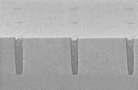
5 of BSI.G05013 coated on via substrates before and after developer etch-back. The bias of isolated and dense areas before develop back is 250 nm (Figure 6a). After 69 seconds of develop back (Figure 6b), the open area and the surface between vias areas are clear. The gap-fill material fully fills the isolated vias and it is only 50 nm below via surface in the dense area. Once the material is developed to the via surface, dissolution rate begins to decrease. This is shown by increasing the develop time by 19 seconds, whereas both the fill and bias did not change considerably (Figure 6c). This attribute provides a large time control margin to process BSI.G Measurements of the SEM pictures Figure 6 gives the dissolution rates of BSI.G05013 above and inside of the vias (Figure 7). Measurements were performed by considering the via top as zero, material above the via top is considered a positive thickness, and below the via top is negative thickness. The slopes of the trend lines present average dissolution rates at dense, isolated, and open areas, which are 5.64 nm/s, 3.64 nm/s, and 1.57 nm/s, respectively. This average dissolution rate difference is the main reason of significant bias reduction. a) Non develop b) Develop 69s c) Develop 88s Figure 6. BSI.G05013 SEM cross-section pictures at different areas, dense via (1.5:1), isolated via (5:1), and open, on SiO2 via wafer. a) no develop, b) develop 69s, c) develop 88s. Figure 7. The measurement from SEM cross-section in Figure 6.


6 Isolated via area Dense via area B L i L d Figure 8. Scheme of thickness measurement. The difference in dissolution rates can be use to form a bias reduction model. Figure 8 represents the initial coating, where B is initial bias, b is final bias, R b is the dissolution rate of bulk material, R v is dissolution rate of the material in the vias, and t develop is develop time. From this, the bias can be expressed as: t develop = L i = L d + b R b R b R v B = b or B R b R v b = R b R v Assuming L i >>L d on the IMEC via substrate and R b >>R v for BSI.G05013 material, the average dissolution rate at dense area is close to the dissolution rate in via R v and dissolution rate at open area is close to the dissolution rate of bulk material R b. Therefore, the bias reduction ratio should be 5.64/1.57=3.59, so it should be possible to reduce bias by 3.59 times on any via substrate using the BSI.G05013 gap-fill material and the develop back process Substrate and BARC compatibility With the continually shrinking semiconductor feature sizes, the distance of interconnect metal lines becomes closer. To conquer the cross talking problem, many kinds of low-k dielectric materials have been developed besides SiO 2. BSI.G05013 had been used to fill different via substrates, such as Fluorinated Spin-on Glass and Black Diamond, and provides the same develop properties and without void formation. a) SiO 2 substrate BSI.G05013/ARC29A BSI.G05013/ARC82A BSI.G05013/DUV42P BSI.G05013/DUV42P b) Black Diamond substrate BSI.G05013/ARC29A BSI.G05013/DUV42P Figure 9. BSI.G05013 applied on SiO 2 and Black diamond via substrates with different BARCs on the top.
 and KrF")


 KrF resist P338 130 nm lines on BARC DUV44 and developed BSI.")
 KrF lithography, b)arf lithography. 3.4. Stability BSI.")

7 Also, it is compatible with BARCs for different wavelength lithography applications. Figure 9 shows BSI.G05013 on two kinds substrates, SiO 2 and Black Diamond, and Brewer Science ArF BARCs (ARC29A and ARC82A) and KrF BARCs (DUV42p and DUV44). The gap-fill material was developed to the via surface and the 60 nm to 90 nm layer of BARC was applied to the top. The surfaces are perfectly flat, and no void formed in the vias. In the situation of developing to the top of vias, resist lines should stand on the surface between vias, where gap-fill material is clean. To be sure of no interaction between gap-fill material and the top layer materials, we performed resist lithography with 100 nm thick BSI.G05013 remaining under the BARC. Three layers above silicon substrate can be seen from the pictures in Figure 10: the top layer is resist lines, the second layer is a BARC layer, and the third layer is BSI.G The resist profile is straight and the depth of focus is broad. The resist lithographic performance is as good as on BARC/Si alone. Resist BARC BSI.G05013 a) KrF resist P nm lines on BARC DUV44 and developed BSI.G05013 stack Resist b) ArF resist AR1682J 80 nm lines on BARC ARC29A and developed BSI.G05013 stack Figure 10. Resist profiles on BARC and developed BSI.G05013 stack, a) KrF lithography, b)arf lithography Stability BSI.G05013 is a very stable product. The two months of aging data in Figure 11 shows no change on thickness or dissolution rate. The accelerated aging test at 35 C also did not show any change. BARC BSI.G05013 Figure 11. Two month aging stored at room temperature and 35 C Spinbowl and solvent compatibility In spin coating process, polymer residue dried in the spin bowl and surround the nozzle must be cleaned by solvents periodically to keep track clean and reduce defects source. We perform spinbowl compatibility tests for this purpose. Wafers are coated and stored open at room temperature for one day to simulate the spinbowl drying condition. Then solvent strip tests carried out and >90% loss represents material spinbowl compatibility. BSI.G05013 is compatible with
8 the solvents commonly used in semiconductor industry, such as PGMEA, PGME, ethyl eactate, acetone, cyclohexane, heptanone, and edge bead cleaners. 4. CONCLUSION The BSI.G05013 developer soluble etch-back gap-fill material developed at Brewer Science provides excellent via fill, isolated and dense bias reduction, and wide process windows. Therefore a wet etch-back gap-fill DD process may provide a better alternative to the currently used plasma etch-back gap-fill process to achieve planar surfaces required for trench lithography. The developer etch-back gap-fill process allows coating, baking, and etch-back to be done in the same track, which eliminates the need to transfer wafers between the etch and photo bays, which increases throughput, reduces defects, and makes the process more cost-effective. 5. REFERENCE Peter Singer, Tantalum, Copper and Damascene: The Future of Interconnects, Semiconductor International, June Robert L. Jackson, Eliot Broadbent, et. Processing and integration of copper interconnects, Solid State Technology, March 1, Owen Hehmeyer, Abhishek Singh, Ramkumar Subramanian, and Joffre Bernard, Bottom anti-reflective coatings: fluid property characterization and wetting tendency, Proceedings of SPIE, vol. 4690, 2002, pp Stanley Wolf, Silicon Processing for the VLSI Era, Volume 4 - Deep-submicron process technology, chapter 15. Sunset Beach, California: Lattice Press, Mireille Maenhoudt, 248nm and 193nm lithography for damascene patterning, IMEC, Leuven, Belgium, Solid State Technology, April, Anwei Qin, New developer-soluble Gap-fill Material with Fast Plasma Etch Rate. SPIE proceeding Volume 6153, Study of Iso/dense Bias of BARCs and Gap-fill Materials on Via Wafers, Rhunhu Huang, SPIE proceeding Volume 6153, 2006.
Hybrid BARC approaches for FEOL and BEOL integration
 Hybrid BARC approaches for FEOL and BEOL integration Willie Perez a, Stephen Turner a, Nick Brakensiek a, Lynne Mills b, Larry Wilson b, Paul Popa b a Brewer Science, Inc., 241 Brewer Dr., Rolla, MO 6541
PROCESS FLOW AN INSIGHT INTO CMOS FABRICATION PROCESS
 Contents: VI Sem ECE 06EC63: Analog and Mixed Mode VLSI Design PROCESS FLOW AN INSIGHT INTO CMOS FABRICATION PROCESS 1. Introduction 2. CMOS Fabrication 3. Simplified View of Fabrication Process 3.1 Alternative
A novel 248-nm wet-developable BARC for trench applications
 A novel 248-nm wet-developable BARC for trench applications Charles J. eef & Deborah Thomas Brewer Science, Inc., 2401 Brewer Dr., Rolla, M, 65401 USA ABSTRACT A novel polyamic acid based, 248-nm wet-developable
Novel Spin on Planarization Technology by Photo Curing SOC (P-SOC)
") Journal of Photopolymer Science and Technology Volume 3, Number 3 (17) 373-378 C 17SPST Technical Paper Novel Spin on Planarization Technology by Photo Curing (P-) Takafumi Endo*, Rikimaru Sakamoto, Keisuke
Journal of Photopolymer Science and Technology Volume 3, Number 3 (17) 373-378 C 17SPST Technical Paper Novel Spin on Planarization Technology by Photo Curing (P-) Takafumi Endo*, Rikimaru Sakamoto, Keisuke
Chapter 2 Manufacturing Process
 Digital Integrated Circuits A Design Perspective Chapter 2 Manufacturing Process 1 CMOS Process 2 CMOS Process (n-well) Both NMOS and PMOS must be built in the same silicon material. PMOS in n-well NMOS
Czochralski Crystal Growth
 Czochralski Crystal Growth Crystal Pulling Crystal Ingots Shaping and Polishing 300 mm wafer 1 2 Advantage of larger diameter wafers Wafer area larger Chip area larger 3 4 Large-Diameter Wafer Handling
EE40 Lec 22. IC Fabrication Technology. Prof. Nathan Cheung 11/19/2009
 Suggested Reading EE40 Lec 22 IC Fabrication Technology Prof. Nathan Cheung 11/19/2009 300mm Fab Tour http://www-03.ibm.com/technology/manufacturing/technology_tour_300mm_foundry.html Overview of IC Technology
MCC. PMGI Resists NANO PMGI RESISTS OFFER RANGE OF PRODUCTS
 MCC PMGI RESISTS OFFER Sub.25µm lift-off processing Film thicknesses from 5µm Choice of resin blends for optimal undercut control High thermal stability Superior adhesion to Si, NiFe, GaAs, InP
Tailorable BARC system to provide optimum solutions for various substrates in immersion lithography
 Tailorable BARC system to provide optimum solutions for various substrates in immersion lithography Michael Swope, Vandana Krishnamurthy, Zhimin Zhu, Daniel Sullivan, Sean Simmons, Chris Cox, Randy Bennett,
Photolithography I ( Part 2 )
") 1 Photolithography I ( Part 2 ) Chapter 13 : Semiconductor Manufacturing Technology by M. Quirk & J. Serda Bjørn-Ove Fimland, Department of Electronics and Telecommunication, Norwegian University of Science
1 Photolithography I ( Part 2 ) Chapter 13 : Semiconductor Manufacturing Technology by M. Quirk & J. Serda Bjørn-Ove Fimland, Department of Electronics and Telecommunication, Norwegian University of Science
Lecture #18 Fabrication OUTLINE
 Transistors on a Chip Lecture #18 Fabrication OUTLINE IC Fabrication Technology Introduction the task at hand Doping Oxidation Thin-film deposition Lithography Etch Lithography trends Plasma processing
9/4/2008 GMU, ECE 680 Physical VLSI Design
 ECE680: Physical VLSI Design Chapter II CMOS Manufacturing Process 1 Dual-Well Trench-Isolated CMOS Process gate-oxide TiSi 2 AlCu Tungsten SiO 2 p-well poly n-well SiO 2 n+ p-epi p+ p+ 2 Schematic Layout
Process Flow in Cross Sections
 Process Flow in Cross Sections Process (simplified) 0. Clean wafer in nasty acids (HF, HNO 3, H 2 SO 4,...) --> wear gloves! 1. Grow 500 nm of SiO 2 (by putting the wafer in a furnace with O 2 2. Coat
Lecture 22: Integrated circuit fabrication
 Lecture 22: Integrated circuit fabrication Contents 1 Introduction 1 2 Layering 4 3 Patterning 7 4 Doping 8 4.1 Thermal diffusion......................... 10 4.2 Ion implantation.........................
EE 5344 Introduction to MEMS. CHAPTER 3 Conventional Si Processing
 3. Conventional licon Processing Micromachining, Microfabrication. EE 5344 Introduction to MEMS CHAPTER 3 Conventional Processing Why silicon? Abundant, cheap, easy to process. licon planar Integrated
EE 330 Lecture 9. IC Fabrication Technology Part 2
 EE 330 Lecture 9 IC Fabrication Technology Part 2 Quiz 8 A 2m silicon crystal is cut into wafers using a wire saw. If the wire diameter is 220um and the wafer thickness is 350um, how many wafers will this
Test Patterns for Chemical Mechanical Polish Characterization
 Dobek S: CMP Characterization 15th Annual Microelectronic Engineering Conference, 1997 Test Patterns for Chemical Mechanical Polish Characterization Stanley 3. Dobek Senior Microelectronic Engineering
EEC 118 Lecture #5: MOS Fabrication. Rajeevan Amirtharajah University of California, Davis Jeff Parkhurst Intel Corporation
 EEC 118 Lecture #5: MOS Fabrication Rajeevan Amirtharajah University of California, Davis Jeff Parkhurst Intel Corporation Announcements Lab 3 this week, report due next week HW 3 due this Friday at 4
Microelectronics. Integrated circuits. Introduction to the IC technology M.Rencz 11 September, Expected decrease in line width
 Microelectronics Introduction to the IC technology M.Rencz 11 September, 2002 9/16/02 1/37 Integrated circuits Development is controlled by the roadmaps. Self-fulfilling predictions for the tendencies
Understanding. Brewer Science
 Understanding ARC Products General ARC Presentation: Slide #1 Overview Anti-reflective coating introduction Types of anti-reflective coating Advantages to anti-reflective coatings Advantages to bottom
Filling and Planarizing Deep Trenches with Polymeric Material for Through-Silicon Via Technology
 Filling and Planarizing Deep Trenches with Polymeric Material for Through-Silicon Via Technology R.K. Trichur, M. Fowler, J.W. McCutcheon, and M. Daily Brewer Science, Inc. 2401 Brewer Drive Rolla, MO
EECS130 Integrated Circuit Devices
 EECS130 Integrated Circuit Devices Professor Ali Javey 9/13/2007 Fabrication Technology Lecture 1 Silicon Device Fabrication Technology Over 10 15 transistors (or 100,000 for every person in the world)
ELEC 3908, Physical Electronics, Lecture 4. Basic Integrated Circuit Processing
 ELEC 3908, Physical Electronics, Lecture 4 Basic Integrated Circuit Processing Lecture Outline Details of the physical structure of devices will be very important in developing models for electrical behavior
ECE321 Electronics I
 ECE321 Electronics I Lecture 19: CMOS Fabrication Payman Zarkesh-Ha Office: ECE Bldg. 230B Office hours: Tuesday 2:00-3:00PM or by appointment E-mail: payman@ece.unm.edu Slide: 1 Miller Effect Interconnect
Isolation of elements
 1 In an IC, devices on the same substrate must be isolated from one another so that there is no current conduction between them. Isolation uses either the junction or dielectric technique or a combination
EE 527 MICROFABRICATION. Lecture 15 Tai-Chang Chen University of Washington EE-527 M4 MASK SET: NPN BJT. C (sub) A E = 40 µm x 40 µm
 A E = 40 µm x 40 µm") EE 527 MICROFABRICATION Lecture 15 Tai-Chang Chen University of Washington EE-527 M4 MASK SET: NPN BJT C (sub) E B A E = 40 µm x 40 µm 1 EE-527 M4 MASK SET: MOS C-V TEST CAPACITORS W = 10 µm L = 10 µm
EE 527 MICROFABRICATION Lecture 15 Tai-Chang Chen University of Washington EE-527 M4 MASK SET: NPN BJT C (sub) E B A E = 40 µm x 40 µm 1 EE-527 M4 MASK SET: MOS C-V TEST CAPACITORS W = 10 µm L = 10 µm
Chapter 3 Silicon Device Fabrication Technology
 Chapter 3 Silicon Device Fabrication Technology Over 10 15 transistors (or 100,000 for every person in the world) are manufactured every year. VLSI (Very Large Scale Integration) ULSI (Ultra Large Scale
EE 330 Lecture 9. IC Fabrication Technology Part II. -Oxidation -Epitaxy -Polysilicon -Planarization -Resistance and Capacitance in Interconnects
 EE 330 Lecture 9 IC Fabrication Technology Part II -Oxidation -Epitaxy -Polysilicon -Planarization -Resistance and Capacitance in Interconnects Review from Last Time Etching Dry etch (anisotropic) SiO
Lecture 19 Microfabrication 4/1/03 Prof. Andy Neureuther
 EECS 40 Spring 2003 Lecture 19 Microfabrication 4/1/03 Prof. ndy Neureuther How are Integrated Circuits made? Silicon wafers Oxide formation by growth or deposition Other films Pattern transfer by lithography
UV15: For Fabrication of Polymer Optical Waveguides
 CASE STUDY UV15: For Fabrication of Polymer Optical Waveguides Master Bond Inc. 154 Hobart Street, Hackensack, NJ 07601 USA Phone +1.201.343.8983 Fax +1.201.343.2132 main@masterbond.com CASE STUDY UV15:
Lecture 1A: Manufacturing& Layout
 Introduction to CMOS VLSI Design Lecture 1A: Manufacturing& Layout David Harris Harvey Mudd College Spring 2004 Steven Levitan Fall 2008 1 The Manufacturing Process For a great tour through the IC manufacturing
Microfabrication of Integrated Circuits
 Microfabrication of Integrated Circuits OUTLINE History Basic Processes Implant; Oxidation; Photolithography; Masks Layout and Process Flow Device Cross Section Evolution Lecture 38, 12/05/05 Reading This
CMOS Manufacturing process. Design rule set
 CMOS Manufacturing process Circuit design Set of optical masks Fabrication process Circuit designer Design rule set Process engineer All material: Chap. 2 of J. Rabaey, A. Chandrakasan, B. Nikolic, Digital
IC/MEMS Fabrication - Outline. Fabrication
 IC/MEMS Fabrication - Outline Fabrication overview Materials Wafer fabrication The Cycle: Deposition Lithography Etching Fabrication IC Fabrication Deposition Spin Casting PVD physical vapor deposition
Microelectronic Device Instructional Laboratory. Table of Contents
 Introduction Process Overview Microelectronic Device Instructional Laboratory Introduction Description Flowchart MOSFET Development Process Description Process Steps Cleaning Solvent Cleaning Photo Lithography
Metallization deposition and etching. Material mainly taken from Campbell, UCCS
 Metallization deposition and etching Material mainly taken from Campbell, UCCS Application Metallization is back-end processing Metals used are aluminum and copper Mainly involves deposition and etching,
Dr. Priyabrat Dash Office: BM-406, Mob: Webpage: MB: 205
 Email: dashp@nitrkl.ac.in Office: BM-406, Mob: 8895121141 Webpage: http://homepage.usask.ca/~prd822/ MB: 205 Nonmanufacturing In continuation from last class... 2 Top-Down methods Mechanical-energy methods
Lab #2 Wafer Cleaning (RCA cleaning)
") Lab #2 Wafer Cleaning (RCA cleaning) RCA Cleaning System Used: Wet Bench 1, Bay1, Nanofabrication Center Chemicals Used: H 2 O : NH 4 OH : H 2 O 2 (5 : 1 : 1) H 2 O : HF (10 : 1) H 2 O : HCl : H 2 O 2
Lab #2 Wafer Cleaning (RCA cleaning) RCA Cleaning System Used: Wet Bench 1, Bay1, Nanofabrication Center Chemicals Used: H 2 O : NH 4 OH : H 2 O 2 (5 : 1 : 1) H 2 O : HF (10 : 1) H 2 O : HCl : H 2 O 2
Complexity of IC Metallization. Early 21 st Century IC Technology
 EECS 42 Introduction to Digital Electronics Lecture # 25 Microfabrication Handout of This Lecture. Today: how are Integrated Circuits made? Silicon wafers Oxide formation by growth or deposition Other
A discussion of crystal growth, lithography, etching, doping, and device structures is presented in
 Chapter 5 PROCESSING OF DEVICES A discussion of crystal growth, lithography, etching, doping, and device structures is presented in the following overview gures. SEMICONDUCTOR DEVICE PROCESSING: AN OVERVIEW
IC Fabrication Technology Part III Devices in Semiconductor Processes
 EE 330 Lecture 10 IC Fabrication Technology Part III Metalization and Interconnects Parasitic Capacitances Back-end Processes Devices in Semiconductor Processes Resistors Diodes Review from Last Lecture
Microelettronica. Planar Technology for Silicon Integrated Circuits Fabrication. 26/02/2017 A. Neviani - Microelettronica
 Microelettronica Planar Technology for Silicon Integrated Circuits Fabrication 26/02/2017 A. Neviani - Microelettronica Introduction Simplified crosssection of an nmosfet and a pmosfet Simplified crosssection
CALTECH CONFERENCE ON VLSI, January 1979
 113 A SIMPLE TWO-LAYER ALUMINUM METAL PROCESS FOR VLSI Robert J. Huber Electrical Engineering Department University of Utah Salt Lake City, Utah 84112 I. Introduction The use of two levels of metal interconnect
Pattern Dependent Satellite Defects in Via Lithography
 Pattern Dependent Satellite Defects in Via Lithography Chih-Chieh Yu*, Mars Yang, Elvis Yang, T. H. Yang, K. C. Chen and Chih-Yuan Lu Macronix International Co. Ltd, No. 16, Li-Hsin Rd., Science Park,
Fabrication Technology
 Fabrication Technology By B.G.Balagangadhar Department of Electronics and Communication Ghousia College of Engineering, Ramanagaram 1 OUTLINE Introduction Why Silicon The purity of Silicon Czochralski
VLSI Design and Simulation
 VLSI Design and Simulation CMOS Processing Technology Topics CMOS Processing Technology Semiconductor Processing How do we make a transistor? Fabrication Process Wafer Processing Silicon single crystal
Overview of Dual Damascene Cu/Low-k Interconnect
 ERC Retreat Stanford: New Chemistries & Tools for scco 2 Processing of Thin Films Overview of Dual Damascene Cu/Low-k Interconnect P. Josh Wolf 1,4 - Program Manager, Interconnect Div. josh.wolf@sematech.org
Use of Spin-On-Hard Mask Materials for nano scale patterning technology
 Use of Spin-On-Hard Mask Materials for nano scale patterning technology Wen-Hao Wu*, Edward Y. Chang, National Chiao Tung University, Department of Materials Science and Engineering 1001 Ta-Hsueh Rd.,
Photoresist-induced development behavior in DBARCs
 Photoresist-induced development behavior in DBARCs Jim D. Meador, Alice Guerrero, Joyce A. Lowes, Charlyn Stroud, Brandy Carr, Anwei Qin, Carlton Washburn, and Ramil-Marcelo L. Mercado Brewer Science,
Lect. 2: Basics of Si Technology
 Unit processes Thin Film Deposition Etching Ion Implantation Photolithography Chemical Mechanical Polishing 1. Thin Film Deposition Layer of materials ranging from fractions of nanometer to several micro-meters
CSCI 4974 / 6974 Hardware Reverse Engineering. Lecture 5: Fabrication processes
 CSCI 4974 / 6974 Hardware Reverse Engineering Lecture 5: Fabrication processes QUIZ 3: CMOS layout Quiz Discussion Rationale If you know how something is put together, you can figure out how to take it
PHYS 534 (Fall 2008) Process Integration OUTLINE. Examples of PROCESS FLOW SEQUENCES. >Surface-Micromachined Beam
 Process Integration OUTLINE. Examples of PROCESS FLOW SEQUENCES. >Surface-Micromachined Beam") PHYS 534 (Fall 2008) Process Integration Srikar Vengallatore, McGill University 1 OUTLINE Examples of PROCESS FLOW SEQUENCES >Semiconductor diode >Surface-Micromachined Beam Critical Issues in Process
PHYS 534 (Fall 2008) Process Integration Srikar Vengallatore, McGill University 1 OUTLINE Examples of PROCESS FLOW SEQUENCES >Semiconductor diode >Surface-Micromachined Beam Critical Issues in Process
ECE 659. Jan M. Rabaey Anantha Chandrakasan Borivoje Nikolic. July 30, Digital EE141 Integrated Circuits 2nd Manufacturing.
 Digital Integrated Circuits A Design Perspective Jan M. Rabaey Anantha Chandrakasan Borivoje Nikolic Manufacturing Process July 0, 00 1 CMOS Process 1 A Modern CMOS Process gate-oxide TiSi AlCu Tungsten
Technology. Semiconductor Manufacturing. Hong Xiao INTRODUCTION TO SECOND EDITION SPIE PRESS
 INTRODUCTION TO Semiconductor Manufacturing Technology SECOND EDITION Hong Xiao TECHNISCHE INFORMATIONSBiBUOTHEK UNIVERSITATSBIBLIOTHEK HANNOVER SPIE PRESS Bellingham,Washington USA Contents Preface to
FABRICATION of MOSFETs
 FABRICATION of MOSFETs CMOS fabrication sequence -p-type silicon substrate wafer -creation of n-well regions for pmos transistors, -impurity implantation into the substrate. -thick oxide is grown in the
EE 330 Lecture 8. IC Fabrication Technology Part II. - Oxidation - Epitaxy - Polysilicon - Interconnects
 EE 330 Lecture 8 IC Fabrication Technology Part II - Oxidation - Epitaxy - Polysilicon - Interconnects Review from Last Time MOS Transistor Bulk Source Gate Drain p-channel MOSFET Lightly-doped n-type
CMOS Technology. Flow varies with process types & company. Start with substrate selection. N-Well CMOS Twin-Well CMOS STI
 CMOS Technology Flow varies with process types & company N-Well CMOS Twin-Well CMOS STI Start with substrate selection Type: n or p Doping level, resistivity Orientation, 100, or 101, etc Other parameters
Cu/low κ. Voids, Pits, and Copper
 Cu/low κ S P E C I A L s, Pits, and Copper Judy B Shaw, Richard L. Guldi, Jeffrey Ritchison, Texas Instruments Incorporated Steve Oestreich, Kara Davis, Robert Fiordalice, KLA-Tencor Corporation As circuit
EE 434 Lecture 9. IC Fabrication Technology
 EE 434 Lecture 9 IC Fabrication Technology Quiz 7 The layout of a film resistor with electrodes A and B is shown. If the sheet resistance of the film is 40 /, determine the resistance between nodes A and
Isolation Technology. Dr. Lynn Fuller
 ROCHESTER INSTITUTE OF TECHNOLOGY MICROELECTRONIC ENGINEERING Isolation Technology Dr. Lynn Fuller Motorola Professor 82 Lomb Memorial Drive Rochester, NY 14623-5604 Tel (585) 475-2035 Fax (585) 475-5041
Department of Electrical Engineering. Jungli, Taiwan
 Chapter 3 Fabrication of CMOS Integrated Circuits Jin-Fu Li Department of Electrical Engineering National Central University Jungli, Taiwan Background Outline The CMOS Process Flow Design Rules Latchup
A novel approach to developer-soluble anti-reflective coatings for 248-nm lithography
 A novel approach to developer-soluble anti-reflective coatings for 248-nm lithography Ramil-Marcelo L. Mercado, Joyce A. Lowes, Carlton A. Washburn, Douglas J. Guerrero Brewer Science, Inc., 2401 Brewer
Manufacturing Process
 Digital Integrated Circuits A Design Perspective Jan M. Rabaey Anantha Chandrakasan Borivoje Nikolic Manufacturing Process July 30, 2002 1 CMOS Process 2 A Modern CMOS Process gate-oxide TiSi 2 AlCu Tungsten
Introduction to Nanoscience and Nanotechnology
 Introduction to Nanoscience and Nanotechnology ENS 463 2. Principles of Nano-Lithography by Alexander M. Zaitsev alexander.zaitsev@csi.cuny.edu Tel: 718 982 2812 Office 4N101b 1 Lithographic patterning
Fabrication Process. Crystal Growth Doping Deposition Patterning Lithography Oxidation Ion Implementation CONCORDIA VLSI DESIGN LAB
 Fabrication Process Crystal Growth Doping Deposition Patterning Lithography Oxidation Ion Implementation 1 Fabrication- CMOS Process Starting Material Preparation 1. Produce Metallurgical Grade Silicon
Improving material-specific dispense processes for low-defect coatings
 Improving material-specific dispense processes for low-defect coatings Nick Brakensiek *a, Jennifer Braggin b, John Berron a, Raul Ramirez b, Karl Anderson b, Brian Smith a a Brewer Science, Inc., 2401
Fabrication and Layout
 ECEN454 Digital Integrated Circuit Design Fabrication and Layout ECEN 454 3.1 A Glimpse at MOS Device Polysilicon Aluminum ECEN 475 4.2 1 Material Classification Insulators Glass, diamond, silicon oxide
Manufacturing Process
 Manufacturing Process 1 CMOS Process 2 A Modern CMOS Process gate-oxide TiSi 2 AlCu Tungsten SiO 2 n+ p-well p-epi poly n-well p+ SiO 2 p+ Dual-Well Trench-Isolated CMOS Process 3 Single-crystal ingot
Semiconductor device fabrication
 REVIEW Semiconductor device fabrication is the process used to create the integrated circuits (silicon chips) that are present in everyday electrical and electronic devices. It is a multiplestep sequence
AZ BARLi II Solvent Compatible Bottom Antireflective Coating for i-line Process. Data Package
 AZ BARLi II Solvent Compatible Bottom Antireflective Coating for i-line Process Data Package AZ BARLi II Coating Material Features, Process, and Performance AZ s bottom antireflective coating material,
EE 330 Lecture 9. IC Fabrication Technology Part II. -Oxidation -Epitaxy -Polysilicon -Planarization -Resistance and Capacitance in Interconnects
 EE 330 Lecture 9 IC Fabrication Technology Part II -Oxidation -Epitaxy -Polysilicon -Planarization -Resistance and Capacitance in Interconnects Review from Last Time IC Fabrication Technology Crystal Preparation
CHAPTER - 4 CMOS PROCESSING TECHNOLOGY
 CHAPTER - 4 CMOS PROCESSING TECHNOLOGY Samir kamal Spring 2018 4.1 CHAPTER OBJECTIVES 1. Introduce the CMOS designer to the technology that is responsible for the semiconductor devices that might be designed
MCC. LOR Lift-Off Resists LOR RESISTS OFFER TYPES OF RESISTS
 MCC LOR RESISTS OFFER Submicron linewidth control Finely tuned undercuts Does not intermix with imaging resists (no scum) Excellent adhesion to Si, NiFe, GaAs, InP and many other III-V and II-VI materials
Removal of JSR THB-S375N Photoresist Using a Photoresist Stripper with an Improved EHS Profile Abstract Key words
 Removal of JSR THB-S375N Photoresist Using a Photoresist Stripper with an Improved EHS Profile Yuanmei Cao, Kimberly Pollard, Travis Acra, Nichelle Gilbert, Richie Peters, Donald Pfettscher Abstract Negative
VLSI INTRODUCTION P.VIDYA SAGAR ( ASSOCIATE PROFESSOR) Department of Electronics and Communication Engineering, VBIT
 Department of Electronics and Communication Engineering, VBIT") VLSI INTRODUCTION P.VIDYA SAGAR ( ASSOCIATE PROFESSOR) contents UNIT I INTRODUCTION: Introduction to IC Technology MOS, PMOS, NMOS, CMOS & BiCMOS technologies. BASIC ELECTRICAL PROPERTIES : Basic Electrical
VLSI INTRODUCTION P.VIDYA SAGAR ( ASSOCIATE PROFESSOR) contents UNIT I INTRODUCTION: Introduction to IC Technology MOS, PMOS, NMOS, CMOS & BiCMOS technologies. BASIC ELECTRICAL PROPERTIES : Basic Electrical
Development of 193-nm wet BARCs for implant applications
 Development of 193-nm wet BARCs for implant applications Jim Meador, Carol Beaman, Joyce Lowes, Carlton Washburn, Ramil Mercado, Mariya Nagatkina, and Charlyn Stroud Brewer Science, Inc., 2401 Brewer Drive,
Compact hybrid plasmonic-si waveguide structures utilizing Albanova E-beam lithography system
 Compact hybrid plasmonic-si waveguide structures utilizing Albanova E-beam lithography system Introduction Xu Sun Laboratory of Photonics and Microwave Engineering, Royal Institute of Technology (KTH),
EE 143 CMOS Process Flow
 EE 143 CMOS rocess Flow CT 84 D D G Sub G Sub S S G D S G D S + + + + - MOS Substrate Well - MOS Substrate EE 143 CMOS rocess Flow CT 85 hotoresist Si 3 4 SiO 2 Substrate selection: moderately high resistivity,
MCC. NANO PMMA and Copolymer
 MCC PRODUCT ATTRIBUTES NANO and Submicron linewidth control (polymethyl methacrylate) is a versatile polymeric material that is well suited Sub 0.1µm imaging for many imaging and non-imaging microelectronic
The Physical Structure (NMOS)
") The Physical Structure (NMOS) Al SiO2 Field Oxide Gate oxide S n+ Polysilicon Gate Al SiO2 SiO2 D n+ L channel P Substrate Field Oxide contact Metal (S) n+ (G) L W n+ (D) Poly 1 3D Perspective 2 3 Fabrication
The Physical Structure (NMOS) Al SiO2 Field Oxide Gate oxide S n+ Polysilicon Gate Al SiO2 SiO2 D n+ L channel P Substrate Field Oxide contact Metal (S) n+ (G) L W n+ (D) Poly 1 3D Perspective 2 3 Fabrication
Method For Stripping Copper In Damascene Interconnects >>>CLICK HERE<<<
 Method For Stripping Copper In Damascene Interconnects Damascene, or acid copper plating baths, have been in use since the mid 19th century on decorative items and machinery.1,2 The process generally uses
Exam 1 Friday Sept 22
 Exam 1 Friday Sept 22 Students may bring 1 page of notes Next weeks HW assignment due on Wed Sept 20 at beginning of class No 5:00 p.m extension so solutions can be posted Those with special accommodation
Figure 2.3 (cont., p. 60) (e) Block diagram of Pentium 4 processor with 42 million transistors (2000). [Courtesy Intel Corporation.
 (e) Block diagram of Pentium 4 processor with 42 million transistors (2000). [Courtesy Intel Corporation.") Figure 2.1 (p. 58) Basic fabrication steps in the silicon planar process: (a) oxide formation, (b) selective oxide removal, (c) deposition of dopant atoms on wafer, (d) diffusion of dopant atoms into exposed
Figure 2.1 (p. 58) Basic fabrication steps in the silicon planar process: (a) oxide formation, (b) selective oxide removal, (c) deposition of dopant atoms on wafer, (d) diffusion of dopant atoms into exposed
Supporting Information: Model Based Design of a Microfluidic. Mixer Driven by Induced Charge Electroosmosis
 Supporting Information: Model Based Design of a Microfluidic Mixer Driven by Induced Charge Electroosmosis Cindy K. Harnett, Yehya M. Senousy, Katherine A. Dunphy-Guzman #, Jeremy Templeton * and Michael
Chapter 2 MOS Fabrication Technology
 Chapter 2 MOS Fabrication Technology Abstract This chapter is concerned with the fabrication of metal oxide semiconductor (MOS) technology. Various processes such as wafer fabrication, oxidation, mask
Cu electroplating in advanced packaging
 Cu electroplating in advanced packaging March 12 2019 Richard Hollman PhD Principal Process Engineer Internal Use Only Advancements in package technology The role of electroplating Examples: 4 challenging
Fabrication Technology, Part I
 EEL5225: Principles of MEMS Transducers (Fall 2003) Fabrication Technology, Part I Agenda: Oxidation, layer deposition (last lecture) Lithography Pattern Transfer (etching) Impurity Doping Reading: Senturia,
AZ BARLi II Solvent Compatible Bottom Antireflective Coating for i-line Process Data Package
 AZ BARLi II Solvent Compatible Bottom Antireflective Coating for i-line Process Data Package The information contained herein is, as far as we are aware, true and accurate. However, no representations
CS/ECE 5710/6710. N-type Transistor. N-type from the top. Diffusion Mask. Polysilicon Mask. CMOS Processing
 CS/ECE 5710/6710 CMOS Processing Addison-Wesley N-type Transistor D G +Vgs + Vds S N-type from the top i electrons - Diffusion Mask Mask for just the diffused regions Top view shows patterns that make
Introduction to Micro/Nano Fabrication Techniques. Date: 2015/05/22 Dr. Yi-Chung Tung. Fabrication of Nanomaterials
 Introduction to Micro/Nano Fabrication Techniques Date: 2015/05/22 Dr. Yi-Chung Tung Fabrication of Nanomaterials Top-Down Approach Begin with bulk materials that are reduced into nanoscale materials Ex:
UT Austin, ECE Department VLSI Design 2. CMOS Fabrication, Layout Rules
 2. CMOS Fabrication, Layout, Design Rules Last module: Introduction to the course How a transistor works CMOS transistors This module: CMOS Fabrication Design Rules CMOS Fabrication CMOS transistors are
EE6303 LINEAR INTEGRATED CIRCUITS AND APPLICATIONS 2 MARK QUESTIONS WITH ANSWERS UNIT I IC FABRICATION
 SRI VENKATESWARA COLLEGE OF ENGINEERING AND TECHNOLOGY TIRUPACHUR DEPARTMENT OFELECTRICAL AND ELECTRONICS ENGINEERING EE6303 LINEAR INTEGRATED CIRCUITS AND APPLICATIONS 1. Define an Integrated circuit.
1.1 Background Cu Dual Damascene Process and Cu-CMP
 Chapter I Introduction 1.1 Background 1.1.1 Cu Dual Damascene Process and Cu-CMP In semiconductor manufacturing, we always directed toward adding device speed and circuit function. Traditionally, we focused
Chapter 4 Fabrication Process of Silicon Carrier and. Gold-Gold Thermocompression Bonding
 Chapter 4 Fabrication Process of Silicon Carrier and Gold-Gold Thermocompression Bonding 4.1 Introduction As mentioned in chapter 2, the MEMs carrier is designed to integrate the micro-machined inductor
Semiconductor Device Fabrication
 5 May 2003 Review Homework 6 Semiconductor Device Fabrication William Shockley, 1945 The network before the internet Bell Labs established a group to develop a semiconductor replacement for the vacuum
In-situ Metrology for Deep Ultraviolet Lithography Process Control
 In-situ Metrology for Deep Ultraviolet Lithography Process Control Nickhil Jakatdar 1, Xinhui Niu, John Musacchio, Costas J. Spanos Dept. of Electrical Engineering and Computer Sciences, University of
Introduction to Lithography
 Introduction to Lithography G. D. Hutcheson, et al., Scientific American, 290, 76 (2004). Moore s Law Intel Co-Founder Gordon E. Moore Cramming More Components Onto Integrated Circuits Author: Gordon E.
Polymer-based Microfabrication
 Polymer-based Microfabrication PDMS SU-8 PMMA Hydrogel 1 Soft Lithography Developed by Whitesides, et. al A set of techniques for microfabrication based on the use of lithography, soft substrate materials
Manufacturing Technologies for MEMS and SMART SENSORS
 4 Manufacturing Technologies for MEMS and SMART SENSORS Dr. H. K. Verma Distinguished Professor (EEE) Sharda University, Greater Noida (Formerly: Deputy Director and Professor of Instrumentation Indian
Improvement of Laser Fuse Processing of Fine Pitch Link Structures for Advanced Memory Designs
 Improvement of Laser Fuse Processing of Fine Pitch Link Structures for Advanced Memory Designs Joohan Lee, Joseph J. Griffiths, and James Cordingley GSI Group Inc. 60 Fordham Rd. Wilmington, MA 01887 jlee@gsig.com