Focused Ion Beam CENTRE INTERDISCIPLINAIRE DE MICROSCOPIE ELECTRONIQUE. Marco Cantoni, EPFL-CIME CIME ASSEMBLEE GENERALE 2007
|
|
|
- Leon Rice
- 6 years ago
- Views:
Transcription
1 Focused Ion CENTRE INTERDISCIPLINAIRE DE MICROSCOPIE ELECTRONIQUE Present situation and vision Marco Cantoni, EPFL-CIME Dual Beam Nova 600 Nanolab from FEI Company FE-SEM & FIB: Ga LMIS 4 Gas Injector Systems Pt deposition (C9H16Pt) SiO2 deposition (TEOS) Insulator Enhanced Etch (XeF2) Selective Carbon Mill (MgSO4) Charge neutralizer system Omniprobe (in situ TEM lamella lift out) Fast Electron Beam Blanker (basic e beam lithography) As a part of the clean room facilities: in clean room environment. CIME: client of CMI with 1 main operator (technical personal), 1 PhD student access on a basis of 1-2 days per week Since April 2004: FIB at CMI EPFL 1


2 Applications Chip Modification Insertion of electrical connection: 1) Removal of isolating layer (milling) 2) Pt deposition (FIB deposition) M. Pavius CMI micro/nano-structuring at the CMI FIB-manufactured AFM-tips 2


3 in-situ lift-out TEM sample preparation of a Si nano-wire M. Pavius,, V. Pott, CMI TEM grid, 3mm diameter TEM, CIME M. Cantoni poly-silicon SiO 2 amorph Si 5nm 3


4 TEM sample preparation Prethinned sample preparation Prethinned sample on TEM-«grid» Rough milling at high currents filling of voids Nb 3 Sn superconductor P-Y. Pfyrter (diploma work) 4


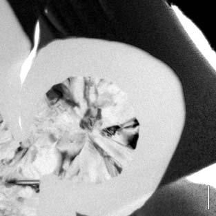
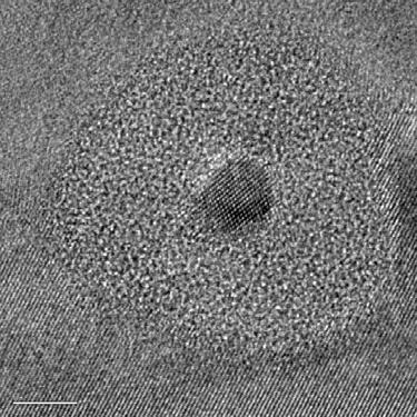
5 2 windows method DF-STEM TEM lamellae preparation by FIB Focused Ion Beam adds a new dimension to TEM specimen preparation But: But: Take Takecare of of artifacts!!!!!! Large flat areas with uniform thickness (50-80 nm) Preparation of heterogeneous samples with difficult material combinations becomes possible Precise selection of the lamella position possible (devices) 5

6 CMI vision: FIB at CIME FIB: indispensable tool for a modern (leading) electron microscopy centre TEM lamellae preparation (50-60%) TEM specimen preparation for analytical TEM and advanced TEM techniques Technical and methodical Research & Development.. TEM lamellae preparation and SEM/STEM (HAADF) + EDX analysis in one machine: increased spatial resolution (approaching TEM resolution) with the ease of use of a SEM. Cross-sectioning of heterogeneous samples, biological samples and soft matter which are not accessible by mechanical preparation methods (polishing or ultramicrotomy). New FIB/SEM techniques (40-50%) Analytical FIB/SEM: cross-sectioning + EDX (on-the-spot) the combination of FIB & analysis offers the great advantage to stay under vacuum in the same machine (oxidization of surface during transfer) 3D-reconstruction (tomography) in BSE mode (mass density contrast) or FIB mode (channeling contrast) of heterogeneous (or porous) samples (for example cement, composite materials, ceramics and polymers). 6
7 vision: FIB at CIME FIB: indispensable tool for a modern (leading) electron microscopy centre TEM lamellae preparation (50-60%) TEM specimen preparation for analytical TEM and advanced TEM techniques Technical and methodical Research & Development.. TEM lamellae preparation and SEM/STEM (HAADF) + EDX analysis in one machine: increased spatial resolution (approaching TEM resolution) with the ease of use of a SEM. Cross-sectioning of heterogeneous samples, biological samples and soft matter which are not accessible by mechanical preparation methods (polishing or ultramicrotomy). chip modification, circuit editing (semiconductor application) prototyping TEM TEM-lamellae for external use (service) No New FIB/SEM techniques (40-50%) Analytical FIB/SEM: cross-sectioning + EDX (on-the-spot) the combination of FIB & analysis offers the great advantage to stay under vacuum in the same machine (oxidization of surface during transfer) 3D-reconstruction (tomography) in BSE mode (mass density contrast) or FIB mode (channeling contrast) of heterogeneous (or porous) samples (for example cement, composite materials, ceramics and polymers). FIB Type: Two Beam Type System requirements e-beam: kV, low voltage compatible (< 1kV) for charging (biological, polymer) samples Ion Beam: 30kV with possibility to work below 5kV (reduction of amorphous layer thickness in TEM lamellae and/or cross-sections for subsequent EBSD Analysis). 1kV if possible. Options: EDX Analysis in FIB configuration Micromanipulators for in-situ TEM lamellae lift-out and handling STEM detector: multi-segment for high-angle annular dark-field (HAADF) or orientation dependent dark-field (ODDF). Software options for automated TEM preparations, cross-sectioning and tomography (unattended over-night use). EBSD for 3D grain orientation analysis (optional, ready for ). 7


 TEST FEI HELIOS")
8 Public call for offers together with ETHZ and PSI, WTO procedure Sept «the ultimate TEM-lamella» (state of the art June 2007) TEST FEI HELIOS Nanolab 600 low kv cleaning at 1kV 8

9 3D Microscopy Journal of Microscopy, Vol. 216, Pt 1 October 2004, pp FIB Nanotomography 9


 align")

10 Preparing for slicing the end Automated milling and imaging of 170 slices (10h) align and crop 10


")
 Ion")

11 3D volume rendering, reconstruction: Orthogonal slices Sagittal slice Coronal slice The choice of the right detector SE detector (TLD) BSE detector (TLD) Ion beam imaging (SE) Ion beam for slicing and imaging requires stage movement! 11


12 Problem of serial sectioning: 3D-reconstruction of disordered microstructures From: J.C.Russ, D 2D Volume fraction?? Nr of particles???? Shape?? DualBeam FIB-Nanotomography Z z-spacing 10 nm Z X Y Electron image: 5 nmresolution Y Stacks with x100 images z-spacing pixel resolution X ème Colloque SFµ Grenoble 2007 atelier FIB Voxel based data volume Reconstruction of microstructure directly in 3D 12

 Drift is often not constant! 0.51503131 Z 0.00104167 0 0.")
 Reference marks 1.")
13 Drift XZ Drift XZ Voxel, Resolution,, Pixel size Drift XZ Drift: 1.5 µm in 6 hrs X (~ 250 nm / hours) Drift is often not constant! Z Drift XZ X ème Colloque SFµ Grenoble 2007 atelier FIB Drift correction: 1.2 Beam shift calibration (V/µm) Reference marks 1.4 Algorithms with pattern recognition Shift beam after each slice


 Quantitative microstructure")

14 Particle recognition: Edge detection in 3D, Watershed for separation Voxel: 75nm Cube: 40* 20* 15 µm Size, 3D-shape, geometrical relationships between particles Grain size fraction 3 Cube size: 23.5x19.2x9.5 µm / Voxel size: 29.69x37.67x60 nm / Nr. of particles: 2236 (total), 1404 (inside) Quantitative microstructure analysis Algorithms Münch and Holzer 2006 J.Amer.Ceram.Soc. FIB-nt of particulate systems part II: Object recognition and effect of boundary truncation 14


15 FIB-nt compared with other 3D-techniques New possibilities in 3D-microscopy: Combination of FIB-nt with Cryo, EDX, EBSD From: Uchic, Holzer and Inkson Mat. Res. Bul., subm. 15
Specimen configuration
 APPLICATIONNOTE Model 1040 NanoMill TEM specimen preparation system Specimen configuration Preparing focused ion beam (FIB) milled specimens for submission to Fischione Instruments. The Model 1040 NanoMill
A New Development to Eliminate Artifacts during TEM Sample Preparation in the FIB
 Inspire Innovation Through Collaboration High Technologies America, Inc. A New Development to Eliminate Artifacts during TEM Sample Preparation in the FIB (Un)traditional FIB Preparation A Common Problem
EBSD Basics EBSD. Marco Cantoni 021/ Centre Interdisciplinaire de Microscopie Electronique CIME. Phosphor Screen. Pole piece.
 EBSD Marco Cantoni 021/693.48.16 Centre Interdisciplinaire de Microscopie Electronique CIME EBSD Basics Quantitative, general microstructural characterization in the SEM Orientation measurements, phase
MODEL NanoMill TEM Specimen Preparation System. Ultra-low-energy, inert-gas ion source. Concentrated ion beam with scanning capabilities
 MODEL 1040 NanoMill TEM Specimen Preparation System The NanoMill system uses an ultra-low energy, concentrated ion beam to produce the highest quality specimens for transmission electron microscopy. Ultra-low-energy,
METHOD FOR IMPROVING FIB PREPARED TEM SAMPLES BY VERY LOW ENERGY Ar + ION MILL POLISHING
 METHOD FOR IMPROVING FIB PREPARED TEM SAMPLES BY VERY LOW ENERGY Ar + ION MILL POLISHING Yaron Kauffmann, Tzipi Cohen-Hyams, Michael Kalina, Hila Sadan-Meltzman and Wayne D. Kaplan Dept. of Materials Engineering
Texture Analysis in MSE
 Texture Analysis in MSE 집합조직제어연구실 서울대학교재료공학부 Texture (Preferred Orientation) Similarity of Texture E.T?! 한쪽을쳐다보고있는사람들여러방향을쳐다보는 Randomly Preferred Oriented What a Wonderful & Beautiful Life! Scientific
Focused Ion Beam (FIB) its principles and applications for materials science. Barbora Bártová
 its principles and applications for materials science. Barbora Bártová") Focused Ion Beam (FIB) its principles and applications for materials science Barbora Bártová Outline 1. Motivation to present FIB-SEM at CERN. 2. Dual beam machine 2.1 Scanning electron microscope (FE-SEM)
Focused Ion Beam (FIB) its principles and applications for materials science Barbora Bártová Outline 1. Motivation to present FIB-SEM at CERN. 2. Dual beam machine 2.1 Scanning electron microscope (FE-SEM)
THREE DIMENSIONAL MICROSTRUCTURAL CHARACTERIZATION OF CATHODE DEGRADATION IN SOFCS USING FOCUSED ION BEAM AND SEM
 THREE DIMENSIONAL MICROSTRUCTURAL CHARACTERIZATION OF CATHODE DEGRADATION IN SOFCS USING FOCUSED ION BEAM AND SEM Joshua Taillon, Christopher Pellegrinelli, Yilin Huang, Eric Wachsman, and Lourdes Salamanca-Riba
John de Laeter Centre
 John de Laeter Centre Major research infrastructure hub at Curtin University, Perth, W.A. ~$30M worth of microscopes, spectrometers, diffractometers and experimental facilities AuScope partner, Microscopy
INITIAL STUDY OF THE MICROSTRUCTURE OF CARBON FIBRES ACTING AS NEGATIVE ELECTRODES IN STRUCTURAL BATTERY COMPOSITES
 Munich, Germany, 26-30 th June 2016 1 INITIAL STUDY OF THE MICROSTRUCTURE OF CARBON FIBRES ACTING AS NEGATIVE ELECTRODES IN STRUCTURAL BATTERY COMPOSITES Fang Liu 1, Masoud Rashidi 2 and Leif E. Asp 3
IBS/e Ion Beam Sputter Deposition and Etching System. IBS/e with KDC-10 Ion Beam Sputter Deposition and Etching System with Kaufman Ion Source
 IBS/e Ion Beam Sputter Deposition and Etching System IBS/e with KDC-10 Ion Beam Sputter Deposition and Etching System with Kaufman Ion Source The Model IBS/e is a high vacuum thin film deposition system
MODEL PicoMill TEM specimen preparation system. Achieve ultimate specimen quality free from amorphous and implanted layers
 MODEL 1080 PicoMill TEM specimen preparation system Combines an ultra-low energy, inert gas ion source, and a scanning electron column with multiple detectors to yield optimal TEM specimens. POST-FIB PROCESSING
Sample Repositioning Solutions for
 Sample Repositioning Solutions for in situ Preparation and Analysis Cheryl Hartfield*, Matt Hammer, Gonzalo Amador, and Tom Moore *Senior Applications Specialist, Omniprobe hartfield@omniprobe.com OUTLINE
In situ TEM Characterization of Shear Stress-Induced Interlayer. Sliding in the Cross Section View of Molybdenum Disulfide
 In situ TEM Characterization of Shear Stress-Induced Interlayer Sliding in the Cross Section View of Molybdenum Disulfide Juan Pablo Oviedo, Santosh KC, Ning Lu, Jinguo Wang, Kyeongjae Cho, Robert M. Wallace,
STRUCTURAL ANALYSIS OF TSVS
 STRUCTURAL ANALYSIS OF TSVS HUGO BENDER CHRIS DRIJBOOMS, PATRICIA VAN MARCKE, JEF GEYPEN, OLIVIER RICHARD, PAOLA FAVIA EFUG2010 Gaeta, 11 October 2010 OUTLINE Introduction : 3D device stacking FIB analysis
Transmission Electron Microscopy (TEM) Prof.Dr.Figen KAYA
 Prof.Dr.Figen KAYA") Transmission Electron Microscopy (TEM) Prof.Dr.Figen KAYA Transmission Electron Microscope A transmission electron microscope, similar to a transmission light microscope, has the following components along
Transmission Electron Microscopy (TEM) Prof.Dr.Figen KAYA Transmission Electron Microscope A transmission electron microscope, similar to a transmission light microscope, has the following components along
Microstructural Characterization of Materials
 Microstructural Characterization of Materials 2nd Edition DAVID BRANDON AND WAYNE D. KAPLAN Technion, Israel Institute of Technology, Israel John Wiley & Sons, Ltd Contents Preface to the Second Edition
Application Note. Sample Protection prior to FIB Processing. related instruments: Leica EM ACE600. Material Research. Life Science Research
 Material Life Science Application Note Sample Protection prior to FIB Processing related instruments: Leica EM ACE600 Medical Industrial Manufacturing Natural Resources 2 Each Atom Really Counts: Protect
Transmission electron microscopy a versatile tool to study the microstructure of HT-PEMFC
 Transmission electron microscopy a versatile tool to study the microstructure of HT-PEMFC Düsseldorf, Germany Christina Scheu Acknowledgement K. Hengge, S. Gleich Max-Planck-Institut für Eisenforschung
Specimen Preparation Technique for a Microstructure Analysis Using the Focused Ion Beam Process
 Specimen Preparation Technique for a Microstructure Analysis Using the Focused Ion Beam Process by Kozue Yabusaki * and Hirokazu Sasaki * In recent years the FIB technique has been widely used for specimen
8.4 BACKSCATTERED ELECTRON IMAGING OF POLISHED SECTIONS
 8.4 BACKSCATTERED ELECTRON IMAGING OF POLISHED SECTIONS [ ] 8.4.1.2 Polishing 8.4.1.3 Coating It is very important to keep the sample in the desiccator to avoid carbonation. [. ]carbonate crystals formed
3D-EBSD an CrossBeam-Systemen
 FIB- Workshop 3.-4. July 2008 3D-EBSD an CrossBeam-Systemen Ulrike Zeile 1, Ali Gholinia 2 and Frank Bauer 3 Arbeitskreis FIB SSOM DGM/DGE ASEM Hotel Seeburg, Luzern, Switzerland 1. Carl Zeiss NTS 2. Oxford
EBSD Electron BackScatter Diffraction Principle and Applications
 EBSD Electron BackScatter Diffraction Principle and Applications Dr. Emmanuelle Boehm-Courjault EPFL STI IMX Laboratoire de Simulation des Matériaux LSMX emmanuelle.boehm@epfl.ch 1 Outline! Introduction!
TED PELLA, INC. Microscopy Products for Science and Industry
 PELCO SILICON NITRIDE, SILICON DIOXIDE, BLANK SILICON SUBSTRATES & APERTURES FOR TEM Clean, Debris-free with Exact 3mm TEM Frame and EasyGrip Edges PELCO Silicon Nitride Support Films for TEM Hydrophilic
CHARACTERIZATION OF SILICON CARBIDE AND PYROCARBON COATINGS FOR FUEL PARTICLES FOR HIGH TEMPERATURE REACTORS (HTR)
") CHARACTERIZATION OF SILICON CARBIDE AND PYROCARBON COATINGS FOR FUEL PARTICLES FOR HIGH TEMPERATURE REACTORS (HTR) D. Hélary 1,2, X. Bourrat 1, O. Dugne 2, G. Maveyraud 1,2, F. Charollais 3, M. Pérez 4,
CHARACTERIZATION OF SILICON CARBIDE AND PYROCARBON COATINGS FOR FUEL PARTICLES FOR HIGH TEMPERATURE REACTORS (HTR) D. Hélary 1,2, X. Bourrat 1, O. Dugne 2, G. Maveyraud 1,2, F. Charollais 3, M. Pérez 4,
Materials Characterization for Stress Management
 Materials Characterization for Stress Management Ehrenfried Zschech, Fraunhofer IZFP Dresden, Germany Workshop on Stress Management for 3D ICs using TSVs San Francisco/CA, July 13, 2010 Outline Stress
Index. Cambridge University Press Focused Ion Beam Systems: Basics and Applications Edited by Nan Yao. Index.
 3D characterization 126, 127 3D deposition 362, 373, 375, 382, 387, 388 3D etching 376 3D reconstruction 173, 234 3D shape 367, 374, 375, 382 3D-CAD 375, 376, 389 accelerated etching 359, 363, 376, 383
SUPPLEMENTARY INFORMATION
 High Electrochemical Activity of the Oxide Phase in Model Ceria- and Ceria-Ni Composite Anodes William C. Chueh 1,, Yong Hao, WooChul Jung, Sossina M. Haile Materials Science, California Institute of Technology,
Electron Microscopy Studies of Niobium Thin Films on Copper
 Electron Microscopy Studies of Niobium Thin Films on Copper Roy Crooks 1, Greg Thompson 2, Robb Morris 2, Michelle Adams Hughes 3, Daudi Waryoba 3, and Peter Kalu 3 1 Black Laboratories, L.L.C., Newport
STUDY & ANALYSIS OF ALUMINIUM FOIL AND ANATASE TITANIUM OXIDE (TiO2) USING TRANSMISSION ELECTRON MICROSCOPY
 USING TRANSMISSION ELECTRON MICROSCOPY") STUDY & ANALYSIS OF ALUMINIUM FOIL AND ANATASE TITANIUM OXIDE (TiO2) USING TRANSMISSION ELECTRON MICROSCOPY Ayush Garg Department of Chemical and Materials Engineering, University of Auckland, Auckland,
STUDY & ANALYSIS OF ALUMINIUM FOIL AND ANATASE TITANIUM OXIDE (TiO2) USING TRANSMISSION ELECTRON MICROSCOPY Ayush Garg Department of Chemical and Materials Engineering, University of Auckland, Auckland,
Supplementary Materials for
 www.sciencemag.org/cgi/content/full/336/6084/1007/dc1 Supplementary Materials for Unidirectional Growth of Microbumps on (111)-Oriented and Nanotwinned Copper Hsiang-Yao Hsiao, Chien-Min Liu, Han-wen Lin,
Microstructure Analysis by Means of the Orthogonallyarranged
 Hitachi Review Vol. 65 (2016), No. 7 201 Special Contributions Microstructure Analysis by Means of the Orthogonallyarranged FIB-SEM Toru Hara, Dr. Eng. OVERVIEW: Serial sectioning using a combined FIB
In-situ Electron Microscopy Mechanical Testing for Steels
 Technical Report UDC 621. 385. 2 : 620. 17 : 669. 14 In-situ Electron Microscopy Mechanical Testing for Steels Shunsuke TANIGUCHI* Gerhard DEHM Abstract This paper outlines the techniques of in-situ electron
Silver Diffusion Bonding and Layer Transfer of Lithium Niobate to Silicon
 Chapter 5 Silver Diffusion Bonding and Layer Transfer of Lithium Niobate to Silicon 5.1 Introduction In this chapter, we discuss a method of metallic bonding between two deposited silver layers. A diffusion
MODEL 1051 TEM Mill ION MILLING. Ion milling is used on physical science. specimens to reduce thickness to electron
 MODEL 1051 TEM Mill A state-of-the-art ion milling and polishing system offering reliable, high performance specimen preparation. It is compact, precise, and consistently produces high-quality transmission
Combining Measurement Methods The Benefit of Fast Analytical Instruments
 Combining Measurement Methods The Benefit of Fast Analytical Instruments Jana Bergholtz, Daniel Goran, Stephan Boehm, René Chemnitzer Bruker Nano GmbH, Berlin, Webinar, October 25 th, 2012 Innovation with
Microscopy and imaging science: practical approaches to applied research and education (A. Méndez-Vilas, Ed.)
") Target preparation and characterization of interfaces in co-sintered metal ceramic composites using imaging and analytical Transmission Electron Microscopy U. Mühle 1,2, A. Günther 1, Y. Standke 1, T.
Target preparation and characterization of interfaces in co-sintered metal ceramic composites using imaging and analytical Transmission Electron Microscopy U. Mühle 1,2, A. Günther 1, Y. Standke 1, T.
Changes in Microstructure of Al/AlN Interface during Thermal Cycling
 Materials Transactions, Vol. 49, No. 12 (2008) pp. 2808 to 2814 #2008 The Japan Institute of Metals Changes in Microstructure of / Interface during Thermal Cycling Yoshiyuki Nagatomo 1, Takeshi Kitahara
Defect and chemical analysis in the TEM
 THE UNIVERSITY Defect and chemical analysis in the TEM Defect and chemical analysis in the TEM I.P. Jones. Chemical analysis: EDX. Chemical analysis: PEELS Centre for Electron Microscopy OF BIRMINGHAM
MODEL 1061 SEM Mill ION MILLING. Ion milling is used in the physical. sciences to enhance the sample s surface. characteristics. Inert gas, typically
 MODEL 1061 SEM Mill A state-of-the-art ion milling and polishing system. It is compact, precise, and consistently produces high-quality scanning electron microscopy (SEM) samples in the shortest amount
Micro-Nano Fabrication Research
 Micro-Nano Fabrication Research Technical Education Quality Improvement Programme 22-23 December 2014 Dr. Rakesh G. Mote Assistant Professor Department of Mechanical Engineering IIT Bombay rakesh.mote@iitb.ac.in;
SUPPLEMENTARY INFORMATIONS
 SUPPLEMENTARY INFORMATIONS Dynamic Evolution of Conducting Nanofilament in Resistive Switching Memories Jui-Yuan Chen, Cheng-Lun Hsin,,, Chun-Wei Huang, Chung-Hua Chiu, Yu-Ting Huang, Su-Jien Lin, Wen-Wei
Specimen Preparation of Metals and Alloys for Atom Probe Tomography by Electropolishing
 Specimen Preparation of Metals and Alloys for Atom Probe Tomography by Electropolishing R. Prakash Kolli, Ph.D., PE July 24, 2016 1st Atom Probe Pre-meeting Congress Organized by the MSA AP FIG 1 Atom
3D Nano-analysis Technology for Preparing and Observing Highly Integrated and Scaled-down Devices in QTAT
 Hitachi Review Vol. 54 (2005), No. 1 27 3D Nano-analysis Technology for Preparing and Observing Highly Integrated and Scaled-down Devices in QTAT Toshie Yaguchi Takeo Kamino Tsuyoshi Ohnishi Takahito Hashimoto
THIN METALLIC LAYERS STRUCTURED BY E-BEAM LITHOGRAPHY. Miroslav HORÁČEK, Vladimír KOLAŘÍK, Michal URBÁNEK, František MATĚJKA, Milan MATĚJKA
 THIN METALLIC LAYERS STRUCTURED BY E-BEAM LITHOGRAPHY Miroslav HORÁČEK, Vladimír KOLAŘÍK, Michal URBÁNEK, František MATĚJKA, Milan MATĚJKA Ústav přístrojové techniky AV ČR, v. v. i., Královopolská 147,
ANALYTICAL SERVICES X-RAY SCATTERING ATOM PROBE TOMOGRAPHY RAMAN SPECTROSCOPY TIME-OF- FLIGHT SECONDARY ION MASS SPECTROMETRY FOCUSED ION BEAM (FIB)
") FRAUNHOFER INSTITUTE FOR PHOTONIC MICROSYSTEMS C ENTER N ANOELECTRONIC TECHNOLOGIES (CNT) Fraunhofer IPMS Center Nanoelectronic Technologies (CNT) Königsbrücker Str. 180 01099 Dresden I Germany www.cnt.fraunhofer.de
FRAUNHOFER INSTITUTE FOR PHOTONIC MICROSYSTEMS C ENTER N ANOELECTRONIC TECHNOLOGIES (CNT) Fraunhofer IPMS Center Nanoelectronic Technologies (CNT) Königsbrücker Str. 180 01099 Dresden I Germany www.cnt.fraunhofer.de
Transzmissziós és pásztázó elektronmikroszkópos minták készítése ionsugaras vékonyítással
 Transzmissziós és pásztázó elektronmikroszkópos minták készítése ionsugaras vékonyítással Radi Zsolt Technoorg Linda Kft., Budapest Oktatói és Doktorandusz Konferencia Visegrád, 2012 State-of-the-art materials
The principles and practice of electron microscopy
 The principles and practice of electron microscopy Second Edition Ian M. Watt CAMBRIDGE UNIVERSITY PRESS Contents Preface tofirstedition page ix Preface to second edition xi 1 Microscopy with light and
Carnegie Mellon MRSEC
 Carnegie Mellon MRSEC Texture, Microstructure & Anisotropy, Fall 2009 A.D. Rollett, P. Kalu 1 ELECTRONS SEM-based TEM-based Koseel ECP EBSD SADP Kikuchi Different types of microtexture techniques for obtaining
Microscopy AND Microanalysis MICROSCOPY SOCIETY OF AMERICA 2007
 Microsc. Microanal. 13, 80 86, 2007 DOI: 10.1017/S1431927607070018 Microscopy AND Microanalysis MICROSCOPY SOCIETY OF AMERICA 2007 High-Quality Sample Preparation by Low kv FIB Thinning for Analytical
A TEM Study on the Microstructure of Fine Flaky Graphite
 Downloaded from orbit.dtu.dk on: May 09, 2018 A TEM Study on the Microstructure of Fine Flaky Graphite Moumeni, Elham; Tiedje, Niels Skat; Horsewell, Andy; Hattel, Jesper Henri Publication date: 2012 Link
ELECTRON MICROSCOPY MODERN SURFACE, LAYER AND DEFECT ANALYSIS USING REM, FIB, EDX, STEM
 FRAUNHOFER INSTITUTE FOR MANUFACTURING ENGINEERING AND AUTOMATION IPA ELECTRON MICROSCOPY MODERN SURFACE, LAYER AND DEFECT ANALYSIS USING REM, FIB, EDX, STEM 1 METHOD Electron microscopy is the favourable
Transmission Kikuchi Diffraction in the Scanning Electron Microscope
 Transmission Kikuchi Diffraction in the Scanning Electron Microscope Robert Keller, Roy Geiss, Katherine Rice National Institute of Standards and Technology Nanoscale Reliability Group Boulder, Colorado
INTEGRATED APPROACH FOR HIGH RESOLUTION SURFACE CHARACTERISATION: COUPLING FOCUSED ION BEAM WITH MICRO AND NANO MECHANICAL TESTS
 Session 10 O_5 Material Characterization INTEGRATED APPROACH FOR HIGH RESOLUTION SURFACE CHARACTERISATION: COUPLING FOCUSED ION BEAM WITH MICRO AND NANO MECHANICAL TESTS E. Bemporad 1, M. Sebastiani 1,
Monday: Y42 G53 Tuesday: Y42 G53 Wednesday: Y42 J11
 Locations: Irchel building 42, Level H and F Locations: Irchel building 42, Level H and F Self-study sessions: Monday: Y42 G53 Tuesday: Y42 G53 Wednesday: Y42 J11 1 Center for Microscopy and Image Analysis
Formation of High-quality Aluminum Oxide under Ion Beam Irradiation
 15th International School-Conference New materials Materials of innovative energy: development, characterization methods and application Volume 2018 Conference Paper Formation of High-quality Aluminum
XTEM characterization of modulated ion implantation through self-organized anodic aluminium oxide (AAO) membranes
 membranes") XTEM characterization of modulated ion implantation through self-organized anodic aluminium oxide (AAO) membranes Wei Guan 1, Jay Ghatak 1, Nianhua Peng 2, Yong Peng 1, Chris Jeynes 2, Beverley Inkson
XTEM characterization of modulated ion implantation through self-organized anodic aluminium oxide (AAO) membranes Wei Guan 1, Jay Ghatak 1, Nianhua Peng 2, Yong Peng 1, Chris Jeynes 2, Beverley Inkson
Microstructure of as-coated thermal barrier coatings with varying lifetimes
 Surface and Coatings Technology 177 178 (2004) 89 96 Microstructure of as-coated thermal barrier coatings with varying lifetimes a a b b, A.J. Burns, R. Subramanian, B.W. Kempshall, Y.H. Sohn * a Siemens-Westinghouse
MODEL SEM Mill. Two independently adjustable TrueFocus ion sources
 MODEL 1060 SEM Mill A state-of-the-art ion milling and polishing system. It is compact, precise, and consistently produces high-quality scanning electron microscopy (SEM) samples for a wide variety of
Multiphase analysis - combining EDS and EBSD
 Multiphase analysis - combining EDS and EBSD Outline Review: Conventional materials characterisation: Analysing polyphase materials using EDS Analysing polyphase materials using EBSD Combined EDS and EBSD
Electrical Characterization of Tungsten Nanowires Deposited by Focused Ion Beam (FIB) *
 *") Nanopages 1 (2006) 2, 255 262 DOI: 10.1556/Nano.1.2006.2.10 Electrical Characterization of Tungsten Nanowires Deposited by Focused Ion Beam (FIB) * E. Horváth 1,2**, P. L. Neumann 2, A. L. Tóth 1, É. Vázsonyi
Nanopages 1 (2006) 2, 255 262 DOI: 10.1556/Nano.1.2006.2.10 Electrical Characterization of Tungsten Nanowires Deposited by Focused Ion Beam (FIB) * E. Horváth 1,2**, P. L. Neumann 2, A. L. Tóth 1, É. Vázsonyi
In-situ Heating Characterisation Using EBSD
 Webinar In-situ Heating Characterisation Using EBSD Speakers Dr. Ali Gholinia Dr. Neil Othen Dr. Jenny Goulden Topics Introduction to EBSD Why do in-situ experiments? EBSD equipment requirements for in-situ
Growth of monocrystalline In 2 O 3 nanowires by seed orientation dependent vapour-solid-solid mechanism
 Electronic Supplementary Material (ESI) for Journal of Materials Chemistry C. This journal is The Royal Society of Chemistry 2014 Electronic Supplementary Information (ESI) Growth of monocrystalline In
Searching for new API Polymorphs Crystal Structure Determination of Pharmaceutical crystals using Electron Diffraction Tomography
 Searching for new API Polymorphs Crystal Structure Determination of Pharmaceutical crystals using Electron Diffraction Tomography Dr. Partha Pratim Das Application Specialist NanoMEGAS SPRL, Belgium This
Effect of titanium on the near eutectic grey iron
 Downloaded from orbit.dtu.dk on: Jun 15, 2018 Effect of titanium on the near eutectic grey iron Moumeni, Elham; Tiedje, Niels Skat; Hattel, Jesper Henri Publication date: 2012 Link back to DTU Orbit Citation
Maxim Integrated Global Failure Analysis (FA)
") Maxim Integrated Global Failure Analysis (FA) Vision Empower industry leading technologies, protect product brand promises, and be the competitive advantage for Maxim Integrated. Mission Deliver timely,
Maxim Integrated Global Failure Analysis (FA) Vision Empower industry leading technologies, protect product brand promises, and be the competitive advantage for Maxim Integrated. Mission Deliver timely,
zyvex TEM Sample Lift-out Using the Zyvex Nanoprober System By Kimberly Tuck, Zyvex Corporation
 TEM Sample Lift-out Using the Zyvex Nanoprober System By Kimberly Tuck, Zyvex Corporation Introduction The Zyvex Nanoprober System, coupled with a focused ion beam (FIB) tool, is a complete solution for
Three-Dimensional Microstructure Reconstruction Using FIB-OIM
 Materials Science Forum Vols. 558-559 (2007) pp. 915-920 online at http://www.scientific.net (2007) Trans Tech Publications, Switzerland Three-Dimensional Microstructure Reconstruction Using FIB-OIM S.-B.
Nanoscale Imaging, Material Removal and Deposition for Fabrication of Cutting-edge Semiconductor Devices
 Hitachi Review Vol. 65 (2016), No. 7 233 Featured Articles Nanoscale Imaging, Material Removal and Deposition for Fabrication of Cutting-edge Semiconductor Devices Ion-beam-based Photomask Defect Repair
Laser Micromachining for Industrial Applications and R&D. 3D-Micromac AG. Symposium on Smart Integrated Systems in Chemnitz. 3D-Micromac AG
 3D-Micromac AG Symposium on Smart Integrated Systems in Chemnitz 1 1 microdice - TLS-Dicing for separation of SiC 2 microprep - for high-throughput microstructure diagnostics 3 About 3D-Micromac AG 2 microdice
In operandi observation of dynamic annealing: a case. Supplementary Material
 In operandi observation of dynamic annealing: a case study of boron in germanium nanowire devices Supplementary Material Maria M. Koleśnik-Gray, 1,3,4 Christian Sorger, 1 Subhajit Biswas, 2,3 Justin D.
Cross sectional TEM analysis of duplex HIPIMS and DC magnetron sputtered Mo and W doped carbon coatings
 Cross sectional TEM analysis of duplex HIPIMS and DC magnetron sputtered Mo and W doped carbon coatings SHARP, J, MULLER, I Castillo, MANDAL, P, ABBAS, A, WEST, G, RAINFORTH, W M, EHIASARIAN, Arutiun
Multi-scale characterization and modelling of damage evolution in nuclear Gilsocarbon graphite
 Multi-scale characterization and modelling of damage evolution in nuclear Gilsocarbon graphite Dong Liu 1, Peter Heard 1, Branko Šavija 2, Gillian Smith 1, Erik Schlangen 2, and Peter Flewitt 1,3 1 Interface
Cross sectional TEM analysis of duplex HIPIMS and DC magnetron sputtered Mo and W doped carbon coatings
 Cross sectional TEM analysis of duplex HIPIMS and DC magnetron sputtered Mo and W doped carbon coatings SHARP, J, MULLER, I Castillo, MANDAL, P, ABBAS, A, WEST, G, RAINFORTH, W M, EHIASARIAN, Arutiun and
Facet-Selective Epitaxy of Compound Semiconductors on
 Supporting Information For: Facet-Selective Epitaxy of Compound Semiconductors on Faceted Silicon Nanowires Max N. Mankin, Robert W. Day, Ruixuan Gao, You-Shin No, Sun-Kyung Kim, Arthur A. McClelland,
Scanning Electron Microscope & Surface Analysis. Wageningen EM Centre Marcel Giesbers
 Scanning Electron Microscope & Surface Analysis Wageningen EM Centre Marcel Giesbers Scanning Electron Microscope & Surface Analysis SEM vs Light Microscope and Transmission EM Secondary Electron Imaging
TOMOGRAPHIC AND HYPERSPECTRAL ANALYSIS OF POROUS THREE-DIMENSIONAL SOLID OXIDE FUEL CELL CATHODES AT MULTIPLE LENGTH SCALES
 TOMOGRAPHIC AND HYPERSPECTRAL ANALYSIS OF POROUS THREE-DIMENSIONAL SOLID OXIDE FUEL CELL CATHODES AT MULTIPLE LENGTH SCALES Joshua Taillon, Christopher Pellegrinelli, Yilin Huang, Eric Wachsman, and Lourdes
Advanced Manufacturing Choices
 Advanced Manufacturing Choices Table of Content Mechanical Removing Techniques Ultrasonic Machining (USM) Sputtering and Focused Ion Beam Milling (FIB) Ultrasonic Machining In ultrasonic machining (USM),
The Study of SEM Examination of Crept Ceramic Samples Prepared by Cross Polishing Method
 The Study of SEM Examination of Crept Ceramic Samples Prepared by Cross Polishing Method Alper Uludag Faculty of Aeronautics and Astronautics Anadolu University Eskisehir, Turkey alperuludag@anadolu.edu.tr
Product Information Version 2.0. ZEISS ORION NanoFab Three Ion Beams for Enhanced Flexibility in Sub-10 nm Fabrication
 Product Information Version 2.0 ZEISS ORION NanoFab Three Ion Beams for Enhanced Flexibility in Sub-10 nm Fabrication Three Ion Beams for Enhanced Flexibility in Sub-10 nm Fabrication Fabricate sub-10
LYRA3 FIB 1.2 nm Ga 50 ev at 30 kev to 30 kev
 LYRA3 1.2 nm at 30 kev 50 ev to 30 kev FIB Ga LYRA3 - Focused ion beam scanning electron microscope for high-performance in nanoengineering LYRA3 is a dual beam system that combines a high-resolution FE-SEM
Imaging with Diffraction Contrast
 Imaging with Diffraction Contrast Duncan Alexander EPFL-CIME 1 Introduction When you study crystalline samples TEM image contrast is dominated by diffraction contrast. An objective aperture to select either
SIMS AND TEM ANALYSIS OF NIOBIUM BICRYSTALS
 SIMS AND TEM ANALYSIS OF NIOBIUM BICRYSTALS P. Maheshwari a,c, C. Zhou a, F. A. Stevie a,, G. R. Myneni b, J. Spradlin b, G. Ciovati b, J. M. Rigsbee c, A. D. Batchelor a,c, and D. P. Griffis a,c a Analytical
Correlative Microscopy - From living cells to 3D electron microscopy A comprehensive workflow approach
 Correlative Microscopy - From living cells to 3D electron microscopy A comprehensive workflow approach Maria Marosvoelgyi, Liesbeth Hekking, Ben Lich, Matthias Geisbauer and Alex de Marco (FEI) Maja Guenthert
Erosion and fuel retention of different RAFM steel grades
 Erosion and fuel retention of different RAFM steel grades Peng Wang 1, Li Qiao 1, Liang Gao 2, Wolfgang Jacob 2, Engang Fu 3 1. Lanzhou Institute of Chemical Physics, Lanzhou, China 2. Max-Planck Institute
Supporting information. In-situ TEM observation of phase transition of nanoscopic patterns on. baroplastic block copolymer film during nanoindentation
 Supporting information In-situ TEM observation of phase transition of nanoscopic patterns on baroplastic block copolymer film during nanoindentation Ara Jo, Gil Ho Gu, Hong Chul Moon, Sung Hyun Han, Sang
In Situ Observation of Dislocation Nucleation and Escape in a Submicron Al Single Crystal
 Supplementary Information for In Situ Observation of Dislocation Nucleation and Escape in a Submicron Al Single Crystal Sang Ho Oh*, Marc Legros, Daniel Kiener and Gerhard Dehm *To whom correspondence
EMAT, University of Antwerp, Groenenborgerlaan 171, B-2020 Antwerp, Belgium
 Materials Science Forum Vol. 583 (2008) pp 277-284 online at http://www.scientific.net (2008) Trans Tech Publications, Switzerland 3D Reconstruction of Ni 4 Ti 3 Precipitates in a Ni 51 Ti 49 Alloy in
Supporting Information
 Supporting Information Fast-Response, Sensitivitive and Low-Powered Chemosensors by Fusing Nanostructured Porous Thin Film and IDEs-Microheater Chip Zhengfei Dai,, Lei Xu,#,, Guotao Duan *,, Tie Li *,,
Nanodiamond-Polymer Composite Fibers and Coatings
 Nanodiamond-Polymer Composite Fibers and Coatings Yury Gogotsi et al. A.J. Drexel Nanotechnology Institute and Department of Materials Science and Engineering Drexel University, Philadelphia, Pennsylvania
> 3d imaging of ceramic CMC for numerical modelling - 91st annual meeting of the DKG - 8. March 2016
 www.dlr.de Chart 1 > 3d imaging of ceramic CMC for numerical modelling - 91st annual meeting of the DKG - 8. March 2016 3-dimensional microstructure characterization of porous ceramic matrix composites
EDX Microanalysis in TEM
 EDX Microanalysis in TEM a) Review (brush-up) Generation and detection of X-rays, SDD detectors b) Quantification EDX in SEM, Interaction volume AF matrix corrections EDX in TEM (Cliff-Lorimer) c) Examples
Introduction to Electron Microscopy Andres Kaech
 Center for Microscopy and Image Analysis Introduction to Electron Microscopy Andres Kaech The types of electron microscopes Transmission electron microscope (TEM) Scanning electron microscope (SEM) 1 The
LYRA3 FIB 1.2 nm Ga 200 ev at 30 kev to 30 kev
 LYRA3 FIB 1.2 nm at 30 kev Ga 200 ev to 30 kev TESCAN Focused Ion Beam Scanning Electron Microscope - LYRA3 This new generation of field emission scanning electron microscopes provides users with the advantages
SEMATECH Symposium Korea 2012 Practical Analysis Techniques of Nanostructured Semiconductors by Electron Microscopy
 SEMATECH Symposium Korea 2012 Practical Analysis Techniques of Nanostructured Semiconductors by Electron Microscopy Jun-Mo Yang, Ph.D. Measurement & Analysis Team National NanoFab Center, Korea Introduction
AFRL-RX-WP-TP
 AFRL-RX-WP-TP-2008-4022 ADVANCED TEM SAMPLE PREPARATION USING LOW ENERGY (PREPRINT) F.J. Scheltens, R. Wheeler IV, and K. Mahalingam UES, Inc. NOVEMBER 2007 Approved for public release; distribution unlimited.
FUSION IN SITU HEATING AND ELECTRICAL. Protochips Quantifiably Better
 FUSION IN SITU HEATING AND ELECTRICAL Protochips Quantifiably Better PtCo Nanoparticle 700 C Image courtesy Oak Ridge National Lab Fullerene STUDY MATERIALS 1200 C Image courtesy CIC nanogune WITH THERMAL
Observation in the GB (Gentle Beam) Capabilities
 Capabilities") A field-emission cathode in the electron gun of a scanning electron microscope provides narrower probing beams at low as well as high electron energy, resulting in both improved spatial resolution and
A field-emission cathode in the electron gun of a scanning electron microscope provides narrower probing beams at low as well as high electron energy, resulting in both improved spatial resolution and
Supplementary Information. Probing of 2 dimensional confinement-induced structural transitions in amorphous oxide thin film
 Supplementary Information Probing of 2 dimensional confinement-induced structural transitions in amorphous oxide thin film Sung Keun Lee 1* and Chi Won Ahn 2 1School of Earth and Environmental Sciences,
Studies of the AZ91 magnesium alloy / SiO 2. - coated carbon fibres composite microstructure. IOP Conference Series: Materials Science and Engineering
 IOP Conference Series: Materials Science and Engineering Studies of the AZ91 magnesium alloy / SiO 2 - coated carbon fibres composite microstructure To cite this article: A Olszówka-Myalska and A Botor-Probierz