The Pennsylvania State University. The Graduate School. Graduate Program in Materials Science and Engineering
|
|
|
- Bryce Wilson
- 6 years ago
- Views:
Transcription
1 The Pennsylvania State University The Graduate School Graduate Program in Materials Science and Engineering CHARACTERIZATION OF LASER FIRED CONTACTS, LASER DOPED EMITTERS, AND FIXED CHARGE PASSIVATION FOR IMPROVED SILICON SOLAR CELLS A Thesis in Materials Science and Engineering by Brittany Lynn Hedrick 2011 Brittany Lynn Hedrick Submitted in Partial Fulfillment of the Requirements for the Degree of Master of Science August 2011
2 ii The thesis of Brittany Lynn Hedrick was reviewed and approved* by the following: Suzanne E. Mohney Professor of Materials Science and Engineering Thesis Co-advisor Joseph R. Flemish Professor of Materials Science and Engineering Thesis Co-advisor S. Ashok Professor of Engineering Science T. DebRoy Professor of Materials Science and Engineering Joan M. Redwing Professor of Materials Science and Engineering Chair, Intercollege Materials Science and Engineering Graduate Degree Program *Signatures are on file in the Graduate School
3 iii ABSTRACT With the introduction of laser processing into silicon solar cell manufacturing, characterization and understanding of laser-material interactions and laser fired device performance is critical. To assess laser doping of the front-side emitters and laser firing of the rear-side contacts of silicon solar cells, several experiments were carried out to create and characterize laser fired contacts (LFCs) and laser doped emitters (LDEs). Additionally, an investigation of fixed charge layers for increased surface passivation performance was performed. A cross-sectioning and selective plating method was developed to characterize the molten region of LFCs created with varying laser firing conditions. Delineation of the geometry and penetration depth of an LFC, within the silicon, was possible with this method, and the oncemolten, laser fired region was measured to depths of tens of microns in the silicon substrate. Investigation of surface topography, diameter, and electrical performance of LFCs was carried out in previous work by Brennan DeCesar, and is briefly reviewed herein. Simulations of LFCs were performed by modeling devices of different diameter and doping densities to replicate trends in experimental resistance data, and to identify the concentration of Al in the fired contact region. Resistances simulated for LFCs modeled with doping densities above 1x10 18 /cm 3 matched best with experimental data, and the resistance of the contacts is dominated by spreading resistance from the heavily doped region (formed through laser firing) into the rest of the wafer. Laser doped emitters were also fabricated and characterized through electrical characterization and cross-sectioning and junction delineation techniques. Doping of the emitters using phosphorus-doped amorphous silicon films, incorporated in the passivation layers, was found to be promising. Depths of LDEs within the silicon were much shallower than those of LFCs, due to the shorter pulse duration used in laser processing (µs rather than ms).
4 iv Passivation of silicon through the introduction of negative fixed charge was investigated using alumina (Al 2 O 3 ) and hafnia (HfO 2 ) films deposited by atomic layer deposition (ALD). Layered structures with SiO x capping films deposited by plasma enhanced chemical vapor deposition (PECVD) were also investigated. Passivation quality was characterized by measuring effective carrier lifetime using microwave photoconductive decay. The longest lifetimes achieved were over 1.5 ms, measured on a sample passivated with 10 nm Al 2 O 3 and 100 nm SiO x after a 5 min 350 C anneal. Fixed charge density was calculated through flat band voltage shifts in C-V measurements made using a mercury probe. Both the Al 2 O 3 and HfO 2 samples exhibited negative fixed charge densities. Samples passivated with thin Al 2 O 3 layers were found to have the largest negative fixed charge densities, up to 1x10 13 /cm 2. Additionally, the creation of an inversion layer due to fixed charge in passivation films deposited on high resistivity silicon substrates was investigated using contactless conductivity measurements and changes in sheet resistance. The presence of an inversion layer was detected by a decrease in sheet resistance and correlated to an increase in effective carrier lifetime for those samples annealed for 5 min at 450 C in a tube furnace, 450 C in a RTA, and 350 C on a hot plate.
5 v TABLE OF CONTENTS List of Figures...vii List of Tables...xi Glossary of Terms...xii Acknowledgements...xv Chapter 1 Introduction... 1 Device Components... 1 Selective Emitters... 3 Rear-Side Contacts... 5 Surface Passivation... 6 Solar Cell Design Improvements and Modern Structures... 8 Solar Cell Structure and Laser Firing Motivation Experiments and Goals Chapter 2 Laser Fired Contacts Literature Review LFC Simulation and Cross-sectioning Goals Cross-sectioning and Junction Delineation Sample Fabrication Processing Procedures Results and Discussion LFC Simulation Device Modeling and Simulation Simulation Results Chapter 3 Laser Doped Emitters Literature Review LDE Experiments Background Characterization I-V Measurements Antimony Doped Samples Phosphorus Doped Samples Curve Comparison Metallization Cross-sectioning and Junction Delineation Results and Discussion... 79
6 vi Chapter 4 Passivation Literature Review Passivation Experiments Film Thickness Experiment: Al 2 O 3 and HfO 2 Layers Lifetime Measurements C-V Measurements Results and Discussion Multi-Layer Passivation Experiment: Al 2 O 3 /SiO x and HfO 2 /SiO x Layers Lifetime Measurements C-V Measurements Results and Discussion Inversion Layer Experiment: Al 2 O 3 and Al 2 O 3 /SiO x Layers Lifetime Measurements C-V Measurements Sheet Resistance Results Results and Discussion Chapter 5 Conclusions and Future Work Conclusions Future Work Bibliography Appendix A Effective Carrier Lifetime Measurements Appendix B C-V Measurements on n-type Wafers Appendix C C-V Measurements from the Inversion Layer Experiment
7 vii LIST OF FIGURES Figure 1-1: Schematic of a standard solar cell adapted from (2) Figure 1-2: Passivated emitter and rear locally diffused cell (PERL) adapted from (2) Figure 1-3: Front surface field, interdigitated back contact, back junction cell (FSF-IBC) adapted from (2) Figure 2-1: Dense array and sample preparation for polishing Figure 2-2: Polishing wheel and angle at which the sample is polished Figure 2-3: Successful cross-section of a row of LFCs and junction delineation between the p-type melt regions and the n-type substrate, sample passivated with a- Si:H/SiO x Figure 2-4: Sample fired at 45 W and 4 ms showing typical morphology of LFCs fired with the IPG 1070 nm single mode fiber laser Figure 2-5: Cross-sections after junction delineation of an LFC (a) fired at 22 W and 19 ms, passivated with a-si:h, and an LFC in image (b) fired at 45 W and 4 ms, passivated with a-si:h/sio x Figure 2-6: Simulated resistance values and experimental resistance values for LFCs Figure 3-1: Passivation and dopant structures Figure 3-2: Image of a LDE array sample Figure 3-3: I-V curve for a diode with series resistance, schematic after (50) Figure 3-4: I-V curves for LDEs on a-si:h passivated Sb sample, 355 nm laser Figure 3-5: I-V curves for LDEs on a-si:h/sio x passivated Sb sample, 355 nm laser Figure 3-6: SEM images of LDEs on a-si:h passivated Sb sample, 355 nm laser Figure 3-7: SEM images of LDEs on a-si:h/sio x passivated Sb sample, 355 nm laser Figure 3-8: SEM images of LDEs on a-si:h passivated Sb sample, 1070 nm laser. The 20 nm scale marker applies to all micrographs not otherwise labeled Figure 3-9: SEM images of LDEs on a-si:h/sio x passivated Sb sample, 1070 nm laser. The 20 nm scale marker applies to all micrographs not otherwise labeled Figure 3-10: SEM images of processed spots on Sb doped (left) a-si:h passivated sample and (right) a-si:h/sio x passivated sample, 1064 nm laser
8 viii Figure 3-11: I-V curves for LDEs on a-si:h/n+ a-si:h passivated sample, 355 nm laser Figure 3-12: SEM images of LDEs on a-si:h/n+a-si:h passivated sample, 355 nm laser Figure 3-13: I-V curves for LDEs on a-si:h/sio x passivated sample, 355 nm laser Figure 3-14: SEM images of LDEs on a-si:h/n+a-si:h/sio x passivated sample, 355 nm laser Figure 3-15: I-V curves for LDEs on a-si:h/n+a-si:h passivated sample, 1070 nm laser Figure 3-16: SEM images of LDEs on a-si:h/n+a-si:h passivated sample, 1070 nm laser Figure 3-17: I-V curves for LDEs on a-si:h/n+a-si:h/sio x passivated sample, 1070 nm laser Figure 3-18: SEM images of LDEs on a-si:h/n+a-si:h/sio x passivated sample, 1070 nm laser Figure 3-19: SEM images and I-V measurements of LDEs on a-si:h/n+ a-si:h sample, 1064 nm laser Figure 3-20: SEM images and I-V measurements of LDEs on a-si:h/n+ a-si:h/sio x sample, 1064 nm laser Figure 3-21: I-V and log(i)-v plots of the best diode characteristics Figure 3-22: Curves for similar LDEs Figure 3-23: Possible locations of probe tip contacting the LDE when taking I-V measurements Figure 3-24: Importance of a SiO x barrier layer for selective metallization of LDEs Figure 3-25: Tensile stresses evidenced in Ni films by peeling Figure 3-26: Pre and post metallization I-V measurements on a pad fired with the 355 nm laser (155 µj) Figure 3-27: Dense array of LDEs fired at 100W and 100 µs on a-si:h/n+ a-si:h sample using a 1070 nm laser Figure 3-28: Cross-section of LDEs processed with a 1070 nm laser at 100 W and 100 µs Figure 3-29: Cross-sectioned LDE sample fired with 1 pulse at µj/pulse with the 355 nm laser Figure 4-1: Cambridge Savannah TM 200 ALD system and the AMAT P-5000 cluster tool
9 ix Figure 4-2: Barnstead Thermolyne hot plate and Temptronic ThermoChuck vacuum chuck Figure 4-3: Microwave photoconductive decay, effective carrier lifetime measurement set up (50) Figure 4-4: Effective carrier lifetime and annealing temperature Figure 4-5: Agilent4284A LCR meter Leighton 2017B mercury probe Figure 4-6: Shift in V FB due to the metal-semiconductor work function difference and fixed charge in the film Figure 4-7: C-V measurement hysteresis Figure 4-8: C-V curves for the Al 2 O 3 passivated samples Figure 4-9: C-V curves of the 8 nm Al 2 O 3 passivated sample after the 350 C anneal and three months later Figure 4-10: C-V curves for the HfO 2 passivated samples Figure 4-11: C-V curves for 8 nm Al 2 O 3 and 9 nm HfO 2 samples capped with 50 nm SiO x Figure 4-12: Cross sectional diagram of the passivation layer stack up Figure 4-13: C-V measurements for 4 nm Al 2 O 3 and 4 nm Al 2 O 3 /50 nm SiO x passivated samples Figure 4-14: Passivation layers on different substrates for lifetime and C-V measurements and sheet resistance measurements Figure 4-15: Stack passivation layer sample Figure 4-16: Effective carrier lifetime vs. annealing treatment: (a) RTA annealing (b) hot plate annealing Figure 4-17: C-V measurements for RTA annealed 4 nm Al 2 O 3 /100 nm SiO x passivated samples Figure 4-18: C-V measurements for the HP and TF annealed 4 nm Al 2 O 3 /100 nm SiO x samples Figure 4-19: C-V measurements of the RTA annealed 7 nm Al 2 O 3 /100 nm SiO x samples Figure 4-20: C-V measurements for HP and TF annealed 7 nm Al 2 O 3 /100 nm SiO x samples Figure 4-21: C-V measurements for RTA annealed 10 nm Al 2 O 3 /100 nm SiO x samples
10 x Figure 4-22: C-V measurement for HP and TF annealed 10 nm Al 2 O 3 /100 nm SiO x samples Figure 4-23: C-V measurements for RTA annealed 4 nm Al 2 O 3 /4 nm SiO x /7 nm Al 2 O 3 /50 nm SiO x samples Figure 4-24: C-V measurements for HP and TF annealed 4 nm Al 2 O 3 /4 nm SiO x /7 nm Al 2 O 3 /50 nm SiO x samples Figure 4-25: Sheet resistance and effective carrier lifetime vs. annealing treatments for 4 nm Al 2 O 3 passivated sample and 4 nm Al 2 O 3 / 100 nm SiO x passivated samples Figure 4-26: Sheet resistance and effective carrier lifetime vs. annealing treatments for 7 nm Al 2 O 3 passivated sample and 7 nm Al 2 O 3 / 100 nm SiO x passivated samples Figure 4-27: Sheet resistance and effective carrier lifetime vs. annealing treatments for 10 nm Al 2 O 3 passivated sample and 10 nm Al 2 O 3 / 100 nm SiO x passivated samples Figure 4-28: Sheet resistance and effective carrier lifetime vs. annealing treatments for samples passivated with the stack structure Figure B-1: C-V measurements of the 8 nm Al 2 O 3 passivated sample Figure B-2: C-V measurements of the 12 nm Al 2 O 3 passivated sample Figure B-3: C-V measurements of the 20 nm Al 2 O 3 passivated sample Figure B-4: C-V measurements of the 35 nm Al 2 O 3 passivated sample Figure B-5: C-V measurements of the 9 nm HfO 2 passivated sample Figure B-6: C-V measurements of the 13 nm HfO 2 passivated sample Figure B-7: C-V measurements of the 22 nm HfO 2 passivated sample Figure C-1: C-V measurements of the 4 nm Al 2 O 3 passivated samples Figure C-2: C-V measurements 7 nm Al 2 O 3 passivated sample Figure C-3: C-V measurements of the 10 nm Al 2 O 3 passivated sample
11 xi LIST OF TABLES Table 2-1: Dimensions of cross-sectioned profiles within the substrate Table 3-1: Sample processing conditions Table 3-2: LDE parameters plotted in Figure Table 4-1: Al 2 O 3 deposition details Table 4-2: HfO 2 deposition details Table 4-3: Effective carrier lifetime for Al 2 O 3 passivated samples Table 4-4: Effective carrier lifetime for HfO 2 passivated samples Table 4-5: Fixed charge density in Al 2 O 3 passivation films Table 4-6: Fixed charge density in HfO 2 passivation films Table 4-7: Lifetime of thin film ALD samples capped with SiO x Table 4-8: Lifetime of the 4 nm Al 2 O 3 and 4 nm Al 2 O 3 /50 nm SiO x passivated samples Table 4-9: Fixed charge density values for the SiO x capped samples Table 4-10: Annealing conditions studied Table 4-11: Effective carrier lifetime measurements for samples across different annealing treatments Table 4-12: Maximum fixed charge densities
12 xii GLOSSARY OF TERMS AC alternating current Al(CH 3 ) 3 trimethylaluminum, precursor for alumina ALD growth Al 2 O 3 aluminum oxide or alumina ALD atomic layer deposition ARC anti-reflection coating, for reduced reflection at a solar cell s surface a-si:h amorphous silicon, hydrogenated a-si 1 x C x amorphous silicon carbide a-sic x amorphous silicon carbide a-sin x :H amorphous silicon nitride, hydrogenated BOE buffered oxide etch, consisting of hydrofluoric acid and ammonium fluoride and DI water BSF back surface field created at the rear side of a cell due to Al metallization C ox capacitance of an oxide C-V measurement capacitance-voltage measurement CVD chemical vapor deposition CZ Czochralski, silicon growth technique DI water de-ionized water e-beam deposition electron-beam deposition EBIC electron beam induced current FESEM field emission scanning electron microscopy FF fill factor FSF-IBC front surface field interdigitated back contact back junction cell FZ float zone, silicon growth technique H 2 hydrogen gas H 2 O water
13 xiii HfO 2 hafnium oxide or hafnia HIT cell Sanyo s high efficiency cell, the heterojunction with intrinsic thin layer device HP hot plate, used for annealing I o saturation current, a measure of recombination in the scr I-V measurement current-voltage measurement J sc short circuit current LBIC light beam induced current measurement LCP laser chemical processing LCR meter impedance, capacitance, resistance meter LDEs laser doped emitters LFCs laser fired contacts LGBC laser grooved buried contacts LIMPID laser induced melting of a pre-deposited impurity doping L-SNMS laser secondary neutral mass spectroscopy m slope of the qnr and scr regions on a log(i)-v plot n+ a-si:h phosphorus doped a-si:h N 2 nitrogen gas N 2 O nitrous oxide gas Nd:YAG laser neodymium-doped yttrium aluminium garnet laser Nd:YVO 4 laser neodymium-doped yttrium orthovanadate laser PECVD plasma enhanced chemical vapor deposition PERC passivated emitter and rear cell PERL passivated emitter and rear locally diffused cell PERT passivated emitter rear totally diffused cell PH 3 phosphine gas
14 xiv Q f fixed charge density qnr quasi neutral region, the p and n-type regions of a diode, away from the junction r s series resistance RTA rapid thermal anneal or annealing furnace scr space charge region, the region of band bending in a diode SEM scanning electron microscopy SiH 4 silane gas SIMS secondary ion mass spectroscopy SiN x silcon nitride deposited by PECVD SiO 2 silicon dioxide, thermally grown silicon oxide SiO x silicon oxide as deposited by PECVD SOD spin on dopant SRV surface recombination velocity TCAD technology computer-aided design TEM transmission electron microscopy TF tube furnace, used for annealing UV LED ultraviolet light emitting diode V FB flat band voltage, the voltage at the transistion point between accumulation and depletion V oc open circuit voltage µ-pcd microwave photoconductive decay φ MS metal-semiconductor work function difference η conversion efficiency
15 xv ACKNOWLEDGEMENTS First, I would like to thank Dave Carlson, Lian Zhou, and the other scientists of BP Solar for their guidance and support of this research. Second, I would like to acknowledge the students with whom I worked on this research project: Brennan DeCesar, for his initial work with LFCs, and Jillian Woolridge, for her continued work on LDEs. Third, I would like to thank my advisors: Suzanne Mohney, for her guidance and expertise, Joe Flemish, for his guidance in the design of experiments and help in the fab, and Ted Reutzel, for his challenging questions and attention to detail. Fourth, I would like to thank all the students in Suzanne s lab group, for their friendship, insight, and support. Finally, I would like to thank all of my friends and family, for their love and encouragement; most of all my parents and my fiancé Wesley. Hebrews 12:1-3.
16 1 Chapter 1 Introduction Device Components Developed in 1954 by researchers at Bell Telephone, the first solar cell for commercial use was fabricated with an efficiency of 6% (1). The cell was based on a diffused p-n junction, fabricated in silicon, that successfully separated charge carriers generated by the absorption of solar radiation (1) (2). From that structure the basic solar cell design was born. In its simplest form a solar cell is intended to maximize the conversion of incident solar energy into electrical energy (2), and to do so any design requires three necessary components: a semiconducting substrate, a p-n junction, and metal/semiconductor contacts. The band gap in a semiconductor allows for certain wavelengths of electromagnetic radiation to be absorbed; those materials used in solar cells are selected to absorb wavelengths corresponding to the solar spectrum. The substrate comprises the active regions of the solar cell where photon absorption takes place and electron and hole charge carriers are generated (3). A homogeneous or heterogeneous p-n junction, or charge separation engine, is required so that photogenerated charge carriers can be separated for current collection. Homogeneous junctions are formed in silicon by doping a region of the bulk n-type (p-type) substrate to be p-type (n-type). Heterogeneous junctions are formed by growing or depositing a different semiconductor material of a different dopant type and bandgap on top of silicon (3) (4). The space charge region (SCR) that forms in the p-n junction serves to separate electrons and holes absorbed in the bulk of the material, making them available for collection (3) (4). The metal/semiconductor contacts of the cell serve to collect the separated photogenerated carriers from the device, and maintain current flow to the external load on the

17 2 cell. These three components, or variations of them, will be found in any solar cell structure. Working together they allow the device to operate. The basic structure of a bulk silicon solar cell is pictured in Figure 1-1. It features a base layer of silicon for light absorption, a rear-side, full area contact for carrier collection, and a frontside emitter region contacted by thin metal finger contacts, to allow incident light into the cell and create a front contact. The front surface the metal grid (as opposed to a full area, blanket metal contact) is necessary to reduce shading and limit optical losses, but it still provides adequate contact area to minimize resistive losses (5). The junction is present on the front surface of the cell in order to more efficiently collect the large number of carriers that are photogenerated where light is first incident on the cell. Surface treatments, such as texturing and the application of an anti-reflection coating, improve light trapping and decrease reflection of impinging radiation. Surface treatments are just one means of engineering to improve device efficiency. Figure 1-1: Schematic of a standard solar cell adapted from (2). The cell in Figure 1-1 utilizes a p-type silicon wafer as the base material, and an n-type doped emitter region. Cells can also be manufactured on n-type wafers with p-type doped emitters. The quality of the cell and its performance is dependent upon the doping of the base
18 3 layer along with structural and process variables including front contact spacing, minority carrier lifetime, and surface recombination velocities of the front and rear-side contacts and surfaces (2). Intrinsic performance of a solar cell hinges on material quality. Values inherent to the material such as carrier mobility and carrier lifetime will govern the maximum efficiency that a solar cell can achieve. A perfect single crystal would yield the best performance, but in the interest of cost savings, aspects of cell design are sometimes cleverly engineered and manufactured in order to obtain as much performance as possible out of less expensive, lower quality materials. Innovative engineering will be required to obtain (1) effective charge separation at the emitter (p-n junctions), (2) efficient carrier collection at the contacts, and (3) excellent front and rear surface passivation. Selective Emitters In a solar cell, light is absorbed in the bulk material and electron and hole charge carriers are generated. Separation of those photogenerated charges takes place in the space charge region of a p-n junction, built into the solar cell at the interface of the emitter layer and the bulk substrate. Nomenclature surrounding solar cells typically terms the emitter as the layer deposited on the substrate to form the junction, but sometimes refers to emitter characteristics in reference to the performance of the p-n junction (6). In the experimental section, use of the term emitter will refer to the doped region on the front side of a cell and the p-n junction thus created. A good quality emitter-base junction essentially acts as a diode, allowing current flow in one direction and separating carriers out of the cell for collection. Emitter junctions need to be rectifying, with little series resistance, low saturation current, and minimal leakage current. To form the front side emitter in a solar cell, a homogenous or heterogeneous p-n junction can be created. A homogeneous junction is formed by heavily doping the front surface of a p-type (n-
19 4 type) cell to be n-type (p-type). A heterogeneous junction is formed by depositing a p-type (ntype) layer of another semiconducting material onto an n-type (p-type) substrate material (3) (4). In conventional solar cell designs the emitter region is heavily doped over the entire front surface (7) (8). Doping is performed through high temperature furnace diffusion to drive an n-type dopant, such as phosphorus (p-type dopant, i.e., boron), present in a phosphorus containing environment or a phosphosilicate glass, into the p-type (n-type) substrate material (7) (8). The high temperature drive-in step is necessary for doping to occur, but can have undesirable effects on yield due to wafer warping and fracture that can occur (8). Furnace diffusion results in uniform doping across the entire front surface, with no selectivity between the active regions of the material and the regions to be metallized (7). The heavy doping in the active window region decreases the short wavelength response of the cell and leads to a reduction in cell efficiency (7) (9). Continued efforts to manufacture high-efficiency cells necessitated a switch to selective emitters, which feature heavily doped contact areas underneath the metallized region and a light doping in the window regions (active regions) between front metal fingers (9) (10). Heavy doping under metal contacts ensures ohmic contact formation and reduced contact resistance, and light doping of the active regions of a cell reduces recombination and improves spectral response (11). Selective emitters are formed through either photolithographic patterning and an etch back process, or screen printing and patterning of a dopant paste or metallization paste with the dopant mixed in (10). The heavily doped regions under the metallization have to be carefully patterned for alignment of the metal fingers that are subsequently patterned over the doped region using screen printing, or in high-efficiency cells photolithographic patterning and electron-beam or physical vapor deposition.
20 5 Rear-Side Contacts Photogenerated majority carriers are collected out of the cell at the rear-side contacts. The contacts need to be low resistance and ohmic to ensure that carriers are collected and to avoid degradation of cell efficiency. Higher resistance contacts hinder the travel of holes (for a p-type cell) through the contact and increase resistive loss. Rear-side contacts can be formed over the full area of the rear or in local areas, depending on the cell structure. Screen printing of the rear side contact is commonly performed due to its low cost (12). Using an aluminum paste, full area contacts are printed and then fired to drive out organics and solvents in the paste. Finally the contact is further annealed to ensure contact of the Al metal with the silicon substrate (7) (12). The aluminum layer aids in the reduction of recombination at the rear surface by generation of a back surface field (BSF), which inhibits the movement of minority carriers to the rear-side surface. The presence of Al, a p-type dopant in Si, generates a p-p+ junction at the rear, from which the localized electric field results (7) (13). While screen printing is inexpensive and repeatable it is undesirable to expose the device to the high temperature firing step required to cure the paste and anneal the contacts. The performance of passivation layers degrades with high temperature firing, and as wafers in production become thinner, the contact printing process and extreme heat treatment required for screen printing can cause wafer warping and breakage (8). In high-efficiency solar cells local rear-side Al contacts are made by photolithographic definition. The contacts must be spaced a certain distance apart in a large array; contact spacing depends on the carrier mobility in the substrate and their diffusion lengths. Contact regions are photolithographically defined and etched through the rear passivation layer, making openings for local metal contact to the active region of the device (12). A blanket layer of aluminum is typically used as the contact metal, deposited through e-beam deposition, thermal evaporation, or sputtering.
21 6 Surface Passivation Surface passivation is critical to solar cell performance because it is at the surface where photo-generated carriers can be most readily lost through recombination (9) (14) (15). In the bulk, electrons and holes exist for a characteristic time before they recombine; referred to as the bulk lifetime, the value is much longer than the near-surface lifetime of the carriers. At the termination of the crystalline silicon lattice, bulk properties of silicon no longer apply and the order and predictability of the lattice is abruptly truncated, leaving dangling bonds, surface states, and numerous defects, which have a large impact on cell efficiency and device performance due to carrier recombination. A large fraction of the photogenerated carriers are generated in the near-surface region as light impinges on the cell, but when electron and hole pairs are generated in the bulk of the cell they must travel to the device contacts to be collected (9). Once in the vicinity of the contacts at the cell surface the carriers have an increased chance of recombination. Electrons and holes are attracted to defect induced traps and surface states instead of the contacts if surface passivation is not in place to mitigate the defects. Passivation and annealing are crucial to reducing carrier recombination and prolonging carrier lifetime. By tying up dangling bonds and reducing the number of defects, device efficiency is increased and carrier collection improved. The passivation layers used must be robust under constant light exposure in outdoor environments, and transparent (on the front side of the cell), to allow light penetration into the cell without absorbing much of the solar spectrum (15). Many materials can be used along with different deposition methods and subsequent heat treatments for passivation. In many solar cells, amorphous silicon (a-si:h) layers or silicon oxide (SiO x ) layers are used for passivation (14). Amorphous silicon layers can degrade over time, with light exposure and heating, due to the breakdown of the silicon-hydrogen in the film (15). The deterioration happens over the course of tens of years, but once it occurs the passivation qualities
22 7 of the film are lost. Amorphous silicon is deposited using plasma enhanced chemical vapor deposition (PECVD). Silicon oxide doubles as an anti-reflection coating (ARC) and a passivation layer. As an ARC it provides enhanced light trapping and light absorption. Silicon dioxide (SiO 2 ) can be grown through thermal oxidation, or SiO x can be deposited using PECVD. Dual layers of a-si:h and SiO x can be used to maximize the benefits of each material and prolong the longevity of the passivation quality. Silicon nitride (SiN x ) is another common material used to provide surface passivation (14). Similar to SiO x, SiN x acts as an ARC, and is deposited through PECVD. Recently amorphous silicon carbide (a-sic x ) has been found to provide suitable passivation of silicon by researchers at Fraunhofer ISE (14) (16) (17). Fixed charge passivation relies on charge in the deposited passivation layer to repel carriers from the surface, in addition to passivation through satisfying dangling bonds and surface states. The main mechanism for passivation is that of field effect passivation; by shielding carriers from the surface, they are never near enough to surface defects to have the opportunity to recombine (15) (18). Negative fixed charge in the passivation film is critical for providing passivation of the surface. Alumina (Al 2 O 3 ) has been reported to have large densities of fixed charge (15) (18), and several groups have demonstrated its use in high-efficiency solar cells. Atomic layer deposition (ALD) and plasma assisted ALD or chemical vapor deposition (CVD) are useful in deposition of Al 2 O 3 passivation layers (15) (19) (20). Film thickness, passivation layer structure, and annealing treatments are important variables in optimizing passivation for increasing carrier lifetime at the surface. Fixed charge passivation potentially could replace conventional passivation materials if proven robust and capable of reducing carrier recombination.
23 8 Solar Cell Design Improvements and Modern Structures In recent years there has been a push to thinner solar cells not only as a result of materials cost, but also due to the performance limitations associated with thicker base materials. If the base layer is excessively thick the photogenerated carriers have more opportunities to recombine within the material before they can be collected at a contact (2). Subsequent generations of solar cells, building upon the bulk crystalline cell, feature device designs and manufacturing techniques to improve performance and cost savings. Thinning the silicon used in the cell is one method to cut costs, but advancements in cell design typically require more expensive manufacturing processes, which are justified only by device performance improvements or cost savings elsewhere (5). To achieve higher conversion efficiencies and reduce manufacturing costs is a challenging combination but ultimately what manufacturers must do. Recently, structures including the heterojunction with intrinsic thin layer (HIT) cell by Sanyo, and rear surface point-contact cells by SunPower, have been commercially manufactured. Sanyo and SunPower have demonstrated cells in production that achieve efficiencies upwards of 20%, with the HIT cell (23%) and rear point contact cell (22.7%), respectively (16) (21). Two additional cell structures that have the potential to defray manufacturing costs and improve device performance are the passivated emitter and rear cell (PERC) and the front surface field interdigitated back contact, back junction cell (FSF-IBC) (14) (22). Coupled with laser manufacturing, the PERC and FSF-IBC structures could lead to significant advancements in cell performance and efficiency (23) (24). The PERC family of cells has achieved some of the highest efficiencies reported. As early as 1990 they were demonstrated with an energy conversion efficiency of 23.1% (25). Shown in Figure 1-2, the passivated emitter and rear locally diffused (PERL) cell features passivation at both the front and rear surfaces along with rear-side diffused p+ regions that serve
24 9 to reduce recombination losses at the contacts (2). PERL cells and passivated emitter rear totally diffused (PERT) cells have been demonstrated by researchers at the University of New South Wales with efficiencies of more than 24% (25). Both are types of PERC cells, featuring localized rear contacts made through the passivating dielectrics. Figure 1-2: Passivated emitter and rear locally diffused cell (PERL) adapted from (2). Creating a heavily doping the region under the contacts makes collection of majority carriers more efficient by the formation of a p-p+ junction and a local back surface field (13). In a PERC cell, the local rear-side contacts can be formed through laser firing, creating highly doped regions like those in a PERL cell, resulting in a BSF due to incorporation of Al into the laser fired contact. Laser firing of PERC cells reduces manufacturing steps and makes them more manufacturable while maintaining high efficiency. The Fraunhofer Institute for Solar Energy Systems has demonstrated PERC cells achieving efficiencies from 20.2 to 22.4% (16) (24) (26). To reduce costs lower quality multi-crystalline silicon is often substituted for single crystalline silicon. The mc-si has shorter minority carrier diffusion lengths and shorter carrier lifetimes, which limit the distance that the photogenerated carriers can travel to reach a contact. The lower quality material dictates the use of a front-side emitter and contact grid to ensure carriers can be collected at the front surface, in the vicinity where they are generated (5).
 shown in Figure 1-3.")
25 10 Unfortunately, the use of front side metal fingers causes shading loss of the active silicon, reducing the area available for photon absorption, leading to a reduction in cell efficiency. An innovative cell design to completely prevent shading loss is the front surface field, interdigitated back contact, back junction cell (FSF-IBC) shown in Figure 1-3. Interdigitating both contacts for collection of electrons and holes (shown as the n+ BSF and the p+emitter) on the rear-side of the cell leaves no metallization in the front side to shadow the active region of the cell (5). Figure 1-3: Front surface field, interdigitated back contact, back junction cell (FSF-IBC) adapted from (2). An n-type substrate is used due to the higher carrier mobilities it features. Higher quality substrates must be used in IBC cells because carriers generated at the front surface must travel from the front surface to the collecting contacts and emitters at the rear-side of the cell (9); therefore, it is critical that minority carrier lifetime and bulk diffusion lengths are very long. As cells become thinner, the quality of the substrate plays an increased role in performance. Since the active region is thinner, the use of a high quality substrate is critical to maintaining device performance (9). Additionally, with the removal of the bulk thickness, carrier collection at the rear of the cell becomes more prevalent, making the FSF-IBC design more attractive (5).
26 11 With increased carrier collection at the rear side, cell performance can be severely limited if recombination at the rear surface and contacts occurs. Passivation at the front and rear surfaces become increasingly important in thinner cells, as well as FSF-IBC cells. In a FSF-IBC cell, excellent surface passivation is important in order to prevent carrier recombination at the front side surface since there are no contacts present to collect them (9). Passivation of the rear surface is important as well since the presence of both contacts means a large concentration of electrons and holes will be in the same area. Recombination at the contacts and front surface must be combatted using field effects (high doping density to create BSFs) and chemical passivation layers (5). Solar Cell Structure and Laser Firing The introduction of laser processing to photovoltaic manufacturing has the potential to be very advantageous for solar cell manufacturability. Laser firing makes possible the formation of front and rear-side contacts in a few steps, rather than the numerous photolithography, development, etching, and metallization steps or the high temperature screen printing steps previously required (24). The formation of front and rear-side contacts through laser firing is one potential method of reducing manufacturing cost while maintaining device performance and improving processing throughput; however, careful control of laser processing conditions must be implemented to ensure that device performance is maintained. It is imperative to understand how lasers processing can be used beneficially for improvement of device performance and implementation in manufacturing. Laser fired contacts (LFCs) rely on a laser to selectively heat and melt regions of the rear Al contact layer through the rear-side passivation layers to create a localized rear-side contact into the underlying silicon substrate. In a PERC type cell this process creates contacts along with a
27 12 localized back surface field (BSFs) created by the incorporation of Al into the molten silicon and subsequent solidification. The BSF positively impacts the recombination dynamics at the rearside contact given that the LFC does not introduce excessive damage to the region around it (16). The primary concern with replacing rear-side solar cell contacts with LFCs is that structural damage can occur due to the large amount of energy imparted by the laser to a very small volume over an exceedingly short time. Excessive laser energy can result in damage to the surrounding substrate and passivation layers, making careful selection of laser processing parameters critical. Conditions for forming LFCs must be only energetic enough to melt and mix the aluminum and silicon in the locally fired contact region; ablation, drilling, or a large heat affected zone are undesirable (27). With careful selection and control of the laser processing parameters, LFCs can be implemented into solar cells structures and can improve cell performance and manufacturing throughput. The doping of locally diffused front side emitters is also possible with the proper implementation of laser firing. So-called laser doped emitters (LDEs) can be fabricated by selectively firing the laser in regions to be metallized. By firing through a dopant layer, a high concentration of the dopant is incorporated into the molten silicon substrate at points selectively melted with a laser (10). Using a laser to dope the emitter has the potential to degrade device performance if the laser processing parameters are excessively energetic. Excessive laser energy can induce defects into the crystalline structure that can act as recombination centers and reduce the number of carriers available for collection (28). In particular, series resistance, saturation current, and leakage current may be affected, and if any one of these parameters is increased, it detracts from the emitter s performance. The diode ideality factor also suffers with increased recombination; therefore, it is critical to perform laser doping with mild processing conditions that do not damage the silicon, but are energetic enough only for adequate doping of the contact, through the passivation layers.
28 13 The passivated emitter and rear cell (PERC) and front surface field interdigitated-back contact (FSF-IBC) cell are particularly well suited for the implementation of laser firing in solar manufacturing. In PERC cells, laser firing has been used to fire rear-side ohmic contacts though passivation layers, incorporating Al into the melted laser fired region of the silicon, forming cells with efficiencies greater than 20% (16) (24) (26). With improved understanding of laser-material interactions and LFE and LDE performance, a fully laser processed cell could be commercially manufactured in the near future. Motivation For solar energy to achieve grid parity, methods to increasing cell efficiency and manufacturability, while minimizing cost, need to be developed. Combining innovative cell structures, like the PERC and FSF-IBC, with advanced processing methods, like laser processing, is one strategy that holds promise in improving solar cell s manufacturability. Laser processing of rear-side contacts and front-side doped emitters, along with the introduction of new passivation techniques, can greatly improve performance of both PERC and FSF-IBC cells, providing efficiency enhancement and eliminating the traditional processing steps for patterning or screen printing emitters and contacts. Using the appropriate processing conditions, laser firing the rearside contacts and laser doping the front-side emitters of crystalline silicon PERC solar cells could be adapted to a low-cost, high-volume manufacturing scenario. Experiments and Goals In order to evaluate the feasibility of laser firing a solar cell and to assess the quality of the resulting contacts and emitters, several experiments have been performed. LFCs were
29 14 fabricated and characterized through cross-sectioning, junction delineation, and simulations of resistance measurements. Two lasers, a ytterbium-doped 1070 nm single mode fiber laser and a Nd:YVO nm frequency tripled Q-switched laser, were utilized to evaluate laser processing parameters. Evaluation of contact geometry within the silicon was carried out using a newly developed technique of cross-sectioning and junction delineation of laser doped features. Device simulations were also performed to estimate the dopant density of the LFCs and to fit experimental current-voltage (I-V) data. Laser doped emitters were fabricated and evaluated through I-V measurements, crosssectioning, and junction delineation. Line emitters are generally studied in the literature, but herein we study individual spot emitters. Fabrication of the LDEs was performed with three different lasers; a ytterbium-doped 1070 nm single mode fiber laser, a Nd:YVO nm frequency tripled solid state Q-switched laser, and a Nd:YAG 1064 nm Q-Switched laser. Diode characteristics were evaluated for each LDE by comparing diode ideality factors, saturation currents, and leakage currents. Cross-sectioning and junction delineation were performed to determine emitter depth and width within the substrate. In passivation layer experiments, alumina (Al 2 O 3 ) and hafnia (HfO 2 ) films prepared by atomic layer deposited (ALD) were investigated as a means of providing fixed charge passivation. Films of varying thickness, and multi-layer structures incorporating plasmaenhanced chemical vapor deposited (PECVD) silicon oxide (SiO x ), were studied with different annealing treatments. Each passivation structure given a different annealing treatment was evaluated through measurement of effective carrier lifetime, calculated fixed charge densities, and sheet resistance changes in special high resistivity wafers, indicating the presence of an inversion layer. Microwave photoconductive decay was used to measure effective carrier lifetime, capacitance-voltage (C-V) measurements were used to calculate fixed charge densities, and a contactless conductivity probe was used to measure sheet resistance.
30 15 In evaluating these devices and passivation layers, the goal was to identify a means to fabricate a fully laser processed, high efficiency cell. Each structure is critical to the device performance and by optimizing each the contacts, emitters, and passivation a high efficiency cell may be manufactured affordably through laser processing.
31 16 Chapter 2 Laser Fired Contacts Literature Review Laser processing has made possible the formation of rear-side ohmic contacts without the use of multi-step photolithography patterning processes previously used in high efficiency solar cells. Instead of opening the rear side dielectric passivation through patterning and etching, and then metalizing the rear contacts, a laser can be used to fire through both the metal and dielectric passivation layers to incorporate the metal into the silicon substrate. Laser fired contacts (LFCs) are also suitable for replacing rear-side contact patterning by screen printing, which requires deposition of a metal paste and a high temperature firing step to create the contact. The elimination of extra processing steps and high temperature steps, along with the potential for compatibility in high efficiency device production has made research in laser processing widely popular. The ability to create laser fired contacts (LFCs) and apply them to solar cell devices has been demonstrated by many research groups (24) (26) (29) (30) (31). The best efficiencies reported have been greater than 18%, with the highest reported being 21.3% and recently 22.4% (14) (16) (24). Devices performance is evaluated by examining solar cell characteristics, including open circuit voltage, V oc, short circuit current, J sc, fill factor, FF, and conversion efficiency, η. However, deeper understanding of the contacts themselves requires further characterization, and groups have used several techniques to do so. The work of Zastrow et al. (23) involved secondary ion mass spectroscopy (SIMS) and transmission electron microscopy (TEM) characterization. LFCs were fired with a pulsed Nd:YAG laser and had diameters between 80 and 100 µm. The group found concentrations of Al on the order of ~10 19 cm -3 at the center of
32 17 the LFC, which was incorporated within the contact to a depth of 1µm (23). Grohe et al. (22) performed laser secondary neutral mass spectroscopy (L-SNMS) as well as electron beam induced current (EBIC) measurements on LFCs fired with a Q-switched Nd:YAG laser. The EBIC and L-SNMS measurements indicated that Al was incorporated with Si in the center region of each contact (22). Additional EBIC measurements on the cross-section of a cleaved LFC confirmed incorporation of the Al within the contact to a depth of ~1µm (22). Kray and Glunz investigated the morphology of LFCs and reported the effects of contact pitch on surface recombination velocity (SRV) analytically and experimentally (32). Surface recombination velocity was determined based on bulk carrier lifetime and near surface carrier lifetime. Light beam induced current (LBIC) measurements, scanning electron microscopy (SEM) images, and EBIC measurements were taken on LFCs to determine the presence of Al in the inner region and measure contact diameter. When performing SEM/EBIC scans on a cross-sectioned LFC fired on n-type silicon, they found Al present within the volume of their contacts as well (32). They report a SRV of 35 cm/s with a contact pitch of 1000µm (32). All these techniques are useful for tracing the presence of Al incorporated into the contacts and prove the ability to create LFCs; however, little has been disseminated with regards to the appropriate laser processing conditions to use. A majority of the LFCs examined in previous work were fired with 1064 nm lasers with nanosecond pulse durations; in research carried out by past students on this project, an investigation to identify processing conditions for 1070 nm and 355 nm lasers was performed (27). Through evaluation of contact resistance, SEM observations, and post-processing effective carrier lifetime measurements, processing conditions of LFCs fabricated with a gated pulse ytterbium-doped 1070 nm single mode fiber laser and with a Nd:YVO nm frequency tripled Q-switched solid-state laser were evaluated for use in manufacturing. Samples investigated were passivated with either 10 nm of amorphous silicon (a-si:h) and 100 nm of silicon oxide (SiO x )
33 18 deposited by plasma-enhanced chemical vapor deposition (PECVD), or 80 nm of a-si:h deposited by PECVD and metallized with a 0.5 µm Al layer deposited on both sides using electron-beam (e-beam) deposition (27). All wafers used for resistance experiments and surface morphology studies were ~275 µm thick (100) p-type float zone (FZ) silicon wafers with a resistivity between 1-5 Ω-cm. LFCs fabricated with each laser were evaluated using SEM imaging to assess visible changes to the contact morphology as a function of laser processing parameters. For the 1070 nm laser, using high power (> 45 W) and long pulse durations (> 14 ms) resulted in large diameter contacts (> 50 µm), and at the largest powers and pulse durations (50 W, 19 ms) degradation of the surrounding area occurred due to a large heat affected zone (27). When low power and short pulse durations were used (< 30 W, and 14 ms), the contacts were much smaller in diameter (< 20 µm) and damage to the surrounding substrate was minimal (27). For the 355 nm laser, using high energies (> 50 µj) and multiple pulses per shot (> 1 pulse) created large contacts and ablated a significant amount of material to the point of laser drilling. Those contacts fired at lower energies (< 50 µj) and single pulses did not penetrate the substrate deeply but still exhibited ablation (27). Following SEM investigation resistance measurements were taken on LFCs fired with each laser to understand the effect of laser processing conditions on the electrical performance. Resistances measured on LFCs fired with the IPG 1070 nm single mode fiber laser correlated inversely with size. The resistance decreased with increased LFC diameter, implying that processing with larger powers and longer pulse duration led to larger contacts with smaller resistances. For the AVIA 355 nm laser, no trends or correlations between resistance and processing conditions were apparent. It was concluded that further investigation of less energetic pulses would be needed to further evaluate the usefulness of the AVIA 355 nm solid state Q-switched laser in LFC manufacturing. Carrier lifetime mapping provided insight into the consequences of laser firing on the effective carrier lifetime. It was demonstrated that appropriate laser firing conditions (30 W and 6.5 ms, 30 W and 21.5 ms, and
34 19 50 W and 4 ms) could be selected to avoid significant degradation of the effective carrier lifetime (27). The lifetime in regions surrounding LFCs processed with the IPG 1070 nm did not degrade after laser processing, but lifetime in regions surrounding LFCs fired with the AVIA 355nm laser did. A 10 min 275 C anneal was required post processing to re-measure lifetime. Having gained an understanding of laser processing conditions useful for LFC creation in this previous work, additional experimentation was needed to understand the laser-material interaction. The work herein sought to study the effects of laser processing conditions on Al incorporation and concentration in the contact, and the resulting geometry of the contact within the silicon substrate. LFC Simulation and Cross-sectioning Goals Based on the experiments performed by DeCesar (27), additional experiments were performed along with simulations, to understand LFC geometry and doping. Cross-sectioning and junction delineation were performed to investigate contact depth within the silicon. A technique was developed to delineate the geometry of the melt region. Simulations using Sentaurus (33) device simulator were carried out to estimate the doping density of the laser fired contacts and fit the experimental trend of reduced contact resistance with increased LFC diameter. LFCs were modeled and resistance measurements were simulated in an attempt to match experimental resistance measurements taken by DeCesar.
35 20 Cross-sectioning and Junction Delineation Sample Fabrication In order to create a p-n junction upon laser firing a p-type Al contact, samples for crosssectioning and junction delineation were fabricated on ~500 µm thick (100) n-type Czochralskigrown (CZ) silicon wafers with a resistivity of Ω-cm. The n-type samples were passivated with either 80 nm of PECVD grown a-si:h or 10 nm of PECVD grown a-si:h and 100 nm of PECVD grown SiO x, and metallized with 0.5 µm of Al deposited on both sides by e-beam deposition. The same ytterbium-doped 1070 nm continuous wave, gated pulse, single mode fiber laser used in previous work was used in fabrication of samples that were cross-sectioned. The 355 nm laser was not investigated due to the poor results previously seen in LFC resistance measurements. Dense arrays of LFCs were fired to increase the likelihood of cross-sectioning multiple contacts on a single sample. Center to center spacing of the LFCs in the array was equal to approximately twice their measured diameter. Processing Procedures Following laser processing, samples were sectioned using a diamond saw for precise control of sample size and orientation. A piece of the sectioned array was super-glued on its face to another silicon piece to protect the edges to be polished from rounding off. The glued sample was mounted onto a polishing stub. The procedure is detailed in Figure 2-1.


36 21 Figure 2-1: Dense array and sample preparation for polishing. By polishing the sample with increasingly finer grits of silicon carbide polishing disks, the sample was gradually ground down and scratches in the surface were polished out. The disks were mounted on a rotating polishing wheel, seen in Figure 2-2, and a steady stream of water was run across them while they spun. Polishing the samples with the LFC array at a slight angle, indicated in Figure 2-2 by θ, increased the likelihood of cross-sectioning more than one LFC. θ Figure 2-2: Polishing wheel and angle at which the sample is polished.
37 22 Throughout the grinding process, the surface was examined under a light microscope to assess the location of the cross-section within the LFC array. The approximate middle of an LFC, where the laser should have melted the silicon to a maximum depth, was reached when the characteristic peaks, at the center of an LFC on the surface, were apparent in cross-section. Once a successful cross-section was made, a final polishing pad was used, and afterwards the sample was rinsed in a de-ionized (DI) water bath and dried with N 2 gas. Techni Gold 25, an electroless plating solution made by Technic, Inc., was used to delineate the p-n junction of the LFCs in a manner similar to that reported for delineating p-n junctions in silicon nanowires (34). Aluminum is a p-type dopant that has solubility on the order of cm -3 in silicon (35) (36). On an n-type wafer the incorporation of Al forms a p-n junction at each laser fired contact, making selective plating possible. Eichfeld et al. successfully demonstrate the selectivity of Technic Gold 25 on very small geometries, delineating n-type sections of 1.4 µm to 0.12 µm lengths on alternating n- and p-type segments of silicon nanowires only 150 nm in diameter (34). Under illumination, gold in the solution selectively plates on the n-type region of the silicon. The n-type region acts as a cathode, due to electrons generated, and the p-type region functions as an anode, remaining free of nucleated gold, due to holes generated. Cross-sectioned samples were immersed in the plating solution and illuminated with a 50 W halogen lamp for 6 to 8 min at room temperature. Once removed from the solution, the samples were rinsed with DI water and dried with nitrogen gas. Imaging the samples in the field emission scanning electron microscope (FESEM) clearly showed the p-type regions created from laser firing, and provided evidence of the presence and incorporation of Al within the laser fired region, seen in Figure 2-3.

38 23 20 µm Figure 2-3: Successful cross-section of a row of LFCs and junction delineation between the p-type melt regions and the n-type substrate, sample passivated with a-si:h/sio x. Results and Discussion Four different samples were cross-sectioned and plated after being processed with the IPG 1070 nm laser. Shown in Table 2-1, two sets of processing conditions were fired onto each type of passivated substrate. The processing conditions, 45 W and 4 ms along with 22 W and 19 ms, were selected to compare the dimensions of the resulting LFCs on each passivation structure. At the higher 45 W power there was not a significant difference in the dimensions of LFCs fired on either substrate, indicating that the structure of the passivation layers did not impact LFC formation. At the lower 22 W power, the LFC fired on the a-si:h passivation structure is slightly larger than the LFC fired on the a-si:h/sio x layer. The difference is slight, but indicates that the presence of the SiO x layer may impact LFC formation at lower powers.
39 24 Table 2-1: Dimensions of cross-sectioned profiles within the substrate. Sample Passivation Power Duration LFC Width LFC Depth n-type a-si:h 5 W 4 ms 57 µm 25 µm n-type a-si:h/sio 2 45 W 4 ms 60 µm 28 µm n-type a-si:h 22 W 19 ms 45 µm 21 µm n-type a-si:h/sio 2 22 W 19 ms 42 µm 16 µm Samples with the 45 W pulse had much larger melt regions than those fired with 22 W, which would be expected. Both sets of processing conditions adequately incorporated aluminum in silicon as evidenced by successful plating of samples. If Al had not been incorporated, there would not have been a noticeable contrast in the plating between n- and p-type regions. It is surmised that the geometry of the p-type region represents the once-molten solidified region, and originates from the melting and mixing of aluminum and silicon during the laser pulse. Solid state diffusion would be negligible given the length of the pulse durations. Aluminum was incorporated within the silicon to depths from 16 to 28 µm, which was much deeper than previously reported (22) (23). Any effect a depletion region may have had on the dimensions has been neglected. Based on the assumed doping concentrations of 1x10 16 /cm 3 for phosphorus in the n-type substrate (from ρ = Ω-cm) and 2x10 19 /cm 3 for Al in the p-type once-molten region (taken from (35)), the depletion width would be less than 0.4 µm wide. The characteristic morphology of LFCs fired with the 1070 nm single mode fiber laser exhibited a peak in the center of a recessed area. LFCs fired at 4 ms and 45 W are seen in Figure 2-4. The figure shows the diameter of the molten region, the diameter of the heat affected zone, and the center peak of the once-molten region. The diameter of the LFC, measured as the visible width of the molten region, is approximately 45 µm.

 was fired at 22 W and 19 ms on an n-type wafer passivated with a- Si:H.")
40 25 Figure 2-4: Sample fired at 45 W and 4 ms showing typical morphology of LFCs fired with the IPG 1070 nm single mode fiber laser. As seen in cross-sectioning, the width of the once molten region is somewhat wider than what is visible at the surface. Figure 2-5 shows the extent of the p-type region for different laser parameters on each type of sample. Both were fired using the IPG 1070 nm single mode fiber laser. The LFC in image (a) was fired at 22 W and 19 ms on an n-type wafer passivated with a- Si:H. The LFC in image (b) fired at 45 W and 4 ms on an n-type wafer passivated with the a- Si:H/SiO x dual stack. In image (b), the characteristic peak seen in the top view of the LFCs in Figure 2-4 is evident in the cross-section. Figure 2-5: Cross-sections after junction delineation of an LFC (a) fired at 22 W and 19 ms, passivated with a-si:h, and an LFC in image (b) fired at 45 W and 4 ms, passivated with a-si:h/sio x.
41 26 LFC Simulation Device Modeling and Simulation To further understand the effects of laser processing parameters on the contact resistance and to determine if experimental measurements could be predicted, LFC simulations were performed using SENTAURUS TCAD by Synopsys, Inc. (33) with the assistance of Brian Downey. Based on the results of cross-sectioning, the LFC device was modeled as a doped hemispherical region embedded at the surface of a silicon substrate. The model was created based on sample geometry, with a wafer thickness of 275µm and length and width of 700 µm on a side. Taking advantage of symmetry, current transport in only one quarter of the contact was simulated, and the total resistance of each LFC was found by dividing the simulated resistance by 4. In order to simulate the boron doped substrate used in experiments, which was measured to have a resistivity of approximately 2 Ω-cm, the modeled substrate was doped p-type with a boron acceptor concentration of 7x10 15 cm -3. Simulations were performed using different doping densities for the contact region to best match the actual doping density of the contact by comparing simulations to experimental measurements. Many papers report aluminum concentrations in silicon similar to the solid solubility limit of 2x10 19 /cm 3, as given by Trumbore in 1960 for a film grown at 800 C (35) (36). However, solubilities from 3x10 19 up to /cm 3 have been suggested for films deposited and annealed at temperatures from C (37) (38) (39). Doping densities up to 1x10 20 /cm 3 were modeled to compare with the experimental data. The device was simulated by applying a dc bias to the top surface area of the LFC region from 0 to 2 V with the entire back side of the substrate at ground. The metal/semiconductor
42 27 contact resistance was neglected in the simulation due to the assumption that Al metal contacts a highly doped p+ region leading to a low specific contact resistance. Those reported in the literature justify this assumption. Hara et al. reported a contact resistivity of 4x10⁻⁶ Ω-cm 2 for an Al sintered contact at 450 C on p+ silicon with a surface dopant concentration of 1x10 19 cm -3 (40). Furthermore, Schwartz reported a contact resistivity of 3.6x10⁻⁶ Ω-cm 2 for laser annealed Al contacts to poly-si (41). A contact resistivity of 4x10⁻⁶ Ω-cm 2 corresponds to a contact resistance of 0.2 Ω for a 25µm radius contact. Such a resistance is much less than the total resistance measured (~100 Ω) and can be neglected. The generated I-V plot produced from the simulation was used to determine the total resistance of each different diameter contact. Simulation Results Simulation of contacts with radii from 10 µm to 40 µm were performed with fixed LFC doping densities of 1x10 16, 1x10 18, 2x10 19 and 1x10 20 /cm 3. The results are shown in Figure 2-6, where simulated resistance values as a function of radius and doping are plotted and compared to experimental data.
43 Resistance (Ω) ms 4 ms 14 ms 19 ms 4 ms 9 ms 19 ms 14 ms 4 ms 1x /cm 3 1x /cm 3 2x /cm 3 1x10²⁰ /cm 3 50W 34W 18W 9 ms 14 ms 19 ms Radius (µm) Figure 2-6: Simulated resistance values and experimental resistance values for LFCs. The simulated total resistance values match well with the experimental data when assuming a doping density of 1x10 18 to 1x10 20 /cm 3 for the LFC region. The experimental resistances for LFCs fired at 34 W match particularly well with the simulated resistances. For a LFC fired at 34 W and 19 ms with a diameter of 19.5 µm the measured resistance was 139 Ω. The simulated resistances of a 20 µm radius LFC with doping from 1x10 18 to 1x10 20 cm -3 were 141 to 137 Ω, matching within +2 Ω. For a LFC fired at 50 W and 19 ms with a radius of 35 µm the measured resistance was 92 Ω. The simulated resistances of a 35 µm radius LFC with doping of 1x10 18 to 1x10 20 /cm 3 were 79 to 76 Ω, a 14% to 17% difference from the measured value. The measured resistance is likely higher than the simulated resistance because of the damage inherent in LFCs fired at larger powers. For a LFC fired at 18 W and 19 ms with a radius of 9.5 µm the measured resistance was 240 Ω. The simulated resistances of a 10 µm radius LFC with doping from 1x10 18 to 1x10 20 /cm 3 were 248 to 215 Ω, a 3% to 10% difference from the measured value.
44 29 For contacts with smaller radii, the doping density of the LFC region has a greater impact on the overall resistance, while contacts with larger radii are less affected by a change in simulated doping density. For the larger radii LFCs simulated with high doping densities, the resistance values begin to coincide despite changes in doping density, because the spreading resistance from the hemispherical p+ region into the substrate dominates the overall resistance. Simulations have shown that the trend seen in experimental resistance measurements, of increased resistance for smaller diameter contacts. Resistances simulated for LFCs modeled with doping densities greater than 1x10 18 /cm -3 matched well, and spreading resistance was found to dominate resistance measurements of larger radii contacts.
45 30 Chapter 3 Laser Doped Emitters Literature Review The advent of laser processing in solar cell manufacturing has led to a wide range of innovative laser-doping techniques for the fabrication of front side emitters (6) (10) (42) (43) (44). In particular, the ability of a laser to locally heat specific regions makes it an ideal tool for doping selective emitters (6) (42) (43) (44). These emitters are located underneath the front side metallization and must have a high doping density to ensure ohmic contact characteristics (6) (11) (44). Lasers are used primarily in two ways: to create either laser-assisted selective emitters or laser doped emitters (LDEs). In the former process, a laser is used to ablate dielectric layers in order to create openings for subsequent doping of the exposed silicon. Doping is performed through conventional furnace diffusion in a subsequent process step (10). In the formation of LDEs, a laser is used to dope select regions (6) (10) (44) (45). Wet or dry processing can be used, the difference being the method of dopant source incorporation into the process (10). In wet processing the dopant material is introduced onto the surface through a liquid stream or in a bath (10) (11). In dry processing the dopant material can be introduced onto the surface through either a gas atmosphere or a dopant containing layer (10). Dopant source layers under investigation in much of the literature include: pure dopant layers (6) (45), spun on dopant layers (42) (44), or even doped amorphous silicon carbide films (16). After introduction of the dopant source to the surface a laser is used to induce doping and dopant activation by melting the substrate, allowing for liquid diffusion of the dopant (6) (10) (11) (42) (44) (45). Once the selective emitter is laser doped, metal fingers must be patterned over the laser doped regions. Previously metallization was performed either by photolithographic patterning
46 31 and subsequent metal deposition (in high efficiency cells), or by careful alignment of a screen printed metal pattern and a high temperature firing step (typical in commercial cells) (12). Photolithographic metal patterning is very expensive but provides well defined, high purity metal contacts. Screen printing is cheap and repeatable but exhibits poor line definition and high resistance lines. The high doping achieved with selective laser doped emitters makes them suitable for electroplating when patterned first with a seed layer (46) (47). Electroplating itself is inexpensive, easily scalable to manufacturing, and provides high purity metallization, but the need for a seed layer when metalizing front side emitter fingers requires an additional deposition step that is undesirable. Selective electroplating techniques are being developed that do not require the use of a seed layer (48), and electroless plating by illumination may also be possible, but neither have been implemented in production. In current research, investigation of metallization processes commonly goes hand in hand with investigation of emitter doping techniques. In work by Kray and McIntosh the formation and performance of selective emitters prepared by laser chemical processing (LCP) was studied (11). A chemical stream directed by a nozzle was used to introduce the liquid dopant material to the cell surface only on regions that were to be laser doped. Deposition of the liquid dopant was followed directly by a scanning laser that melted the selected regions, inducing liquid state diffusion of the dopant into the underlying silicon through the front passivation layers (10) (11). The front side emitters were defined by laser doping and selective heating/melting rather than by photolithographic definition and high temperature diffusion doping in a furnace (11). Kray and McIntosh investigated the I-V characteristics of the LCP grooves and determined the recombination current density (saturation current density) associated with them was at most 8.5x10⁻¹³ A/cm 2 (11). In manufacturing test cells, they achieved efficiencies from 14.6 to 20.4% across planar and textured substrates, demonstrating the compatibility of LCP with manufacturing high-efficiency solar cells (11).
47 32 An additional investigation of LCP and metallization by aerosol jet printing (AJP) was reported by Drew et al. (47). They successfully implemented LCP to create selective emitters, and used AJP to write a silver seed layer over the laser doped regions. The Ag seed layer was then thickened by light induced plating to create a silver metal contact finger 45 to 55 µm wide and 9 µm thick (47). They used laser fluences in the range of 0.5 to 1.5 J/cm 2 to create the emitters but noted a decrease in cell performance when processing with fluences in the range of 1.1 to 1.4 J/cm 2. They attributed performance loss to laser induced damage resulting from higher fluences (47). In studying morphology of the LCP area, they observed that a rough surface was formed rather than a deep groove. Lower fluences made possible the formation of a molten region of silicon in which the dopant material could diffuse and solidify, without material loss through ablation. Higher fluences were attributed to silicon evaporation and removal material from the substrate, forming grooves and material damage rather than doping (47). A concept recently demonstrated at Fraunhoffer ISE, by Suwito et al., used a doped a- Si 1 x C x layer to act as both a passivation layer and dopant source (16). Their so-called passdop layer demonstrated the capability of a dopant source layer to additionally provide surface passivation. Upon laser firing through the layer, melting and liquid dopant diffusion occurred (16). Since the layer doubles as a passivation layer, the removal of an extraneous dopant source layer was not needed. While they used the layer to create rear-side contacts, a similar process commonly referred to as laser induced melting of a pre-deposited impurity doping (LIMPID) (10) (49) is used for doping front-side emitters by firing through a dopant source film. Esturo-Breton et al. fabricated cells with efficiencies of 14.2% by doping selective emitters through a spin on dopant (SOD) layer. A phosphorus containing SOD was deposited and cured producing a 400 nm thick dopant source layer. Selective LDEs were processed using a 15 ns pulsed frequency doubled Nd:YVO 4 laser with a 532 nm wavelength (44). The frequency of the laser was kept under 100 khz and the power used was less than 1 W. The shape of the laser beam in the study was elongated into a line. Energy distribution across the beam remained
48 33 Gaussian, but it was 5µm wide in the y-direction and 200 µm wide in the x-direction. To investigate the concentration and distribution of phosphorus atoms laterally and in the depth of the emitter, secondary ion mass spectroscopy (SIMS) and electron beam induced current (EBIC) measurements were taken. Through SIMS it was determined that laser doping created a heavily doped, shallow emitter, and that the depth of the emitter (250 to 625 nm) increased with pulse energy density (from 2.5 to 4.5 J/cm 2 ) (44). Phosphorus concentrations at the surface were /cm 3 and were on the order of /cm 3 at the depth of 250 nm for the LDE fired at 2.5 J/cm 2. Through transmission electron microscopy (TEM) of the LDE fired at 2.5 J/cm 2 it was observed that the once-molten silicon re-crystallized free of defects; none were apparent in TEM micrographs (44). In evaluating I-V measurements Esturo-Breton et al. observed a double diode behavior, which they attributed to non-uniform lateral distribution of dopants across the doped emitter. They present a two diode model, to match their experimental measurements, in which a heavily doped diode contributed most of the current at high positive voltages and a lightly doped diode contributed at low positive voltages (44). Each diode had an associated series resistance and saturation current; those in the highly doped diode were less than those in the lightly doped diode. The authors attribute the reduced resistance and saturation current seen at higher voltages to the highly doped diode, and increased current flow enabled by the larger area associated with it. The ideality factors associated with the lightly doped diode that dominated at low voltage and the highly doped diode that dominated at high voltage were 2.15 and 3.05, respectively. The model of an emitter is more commonly discussed in terms of a quasi neutral region and space charge region associated with one diode (50), but the model presented by Esturo-Breton et al. fit their experimental data well. Using a 355 nm wavelength laser, Ogane et al. evaluate the formation of LDEs and the effects of laser power on doping depth and concentration. The laser used was a Nd: YAG laser with pulse durations of 15 ns and output power from 0.30 W to 0.55 W (0.51 to 0.93 J/cm 2 ). Comparing both phosphorus and boron SODs, they fabricated emitters on p-type wafers and
49 34 examined the doping of both n+ and p+ emitters, respectively (8). By controlling the power of the laser they were able to alter the depth of the doped emitter region. SIMS measurements indicated that shallower emitters were formed with less powerful laser shots. For a 0.30 W pulse the depth of the emitter, with a concentration of /cm 3, was approximately 70 nm, whereas for a 0.55 W pulse the depth of the emitter, to a concentration of /cm 3, was approximately 230 nm. The highest doping concentrations in the very near surface (within 0.3 µm) were /cm 3 to /cm 3 for phosphorus and /cm 3 to /cm 3 for boron (8). At low powers they found that the performance was limited due to inadequate doping, and at higher powers ablation of the silicon occurred and surface recombination increased, degrading performance. The best results were obtained for cells doped with powers between 0.45 and 0.5 W, but the maximum cell efficiency obtained was 8%. In I-V measurements of the p-n junctions formed by laser doping, an increase in series resistance and leakage current was apparent as compared to junctions created through thermal diffusion. (8). The authors cite crystalline disorder, doping inhomogeneity, and incorporation of carbon or oxygen impurities as sources for reduced performance. Eisele et al., at the University of Stuttgart, demonstrated the LIMPID procedure to create a full area laser doped silicon cell with 18.9 % efficiency (6). The predeposited dopant layer consists of a 60 nm sputter deposited phosphorus film. An 532 nm Nd:YAG laser with a pulse duration 65 ns was used to dope the entire emitter layer on the front surface. The laser pulse melted the surface to a depth of 1 µm, enabling liquid diffusion of the phosphorus dopant (6). In this case, a full area emitter was fabricated instead of selective emitters. The authors did not address any performance loss due to decreased spectral response typically associated with high doping over the entire emitter surface. The cell that achieved 18.9% was of a passivated emitter and rear cell (PERC) type, with SiO 2 passivation at the front and rear surfaces. The cell achieved a very low saturation current density of 88 fa/cm 2 and a short circuit current density (J sc ) of 35 ma/cm 2. The authors state that, theoretically, an open circuit voltage (V oc ) of 694 mv and J sc of 40 ma/cm 2 could be attained if front surface texture and improvement of the rear side contacts
50 35 were implemented. With such improvements they projected an efficiency of 21 % to be possible (6). Given the low J sc and high V oc attainable, Eisele et al. claimed that laser doping did not lead to any lattice defects, and any degradation in cell performance did not result from laser processing the emitter (6). They identified recombination at the rear side contact to be the main source of performance loss in the cell. On the other hand, Ametowobla et al. attempted to identify the effects of laser doping on device performance by laser irradiating samples with and without a dopant layer on the surface, and highlighted several factors that must be controlled to ensure device performance. They hypothesized initially that discrepancies between theoretically attainable V oc values and those measured in actual cells were due to recombination in the doped emitters due to laser processing (28). By examining saturation current densities and SIMS profiles, they identified two factors that degraded device performance. The first was the choice of dopant precursor. Through evaluation of different doping precursors it was discovered that the choice of dopant source greatly influenced recombination in the emitter. If ultrapure doping precursors were not used, impurities in the precursors were incorporated into the doped emitter and led to increased saturation current densities. The second factor was the laser irradiation on the sample. When irradiating pre-diffused emitters without a dopant layer in place an increase in recombination was noted. Defects inherent to the laser firing process occurred, resulting in more recombination, increasing the saturation current density from 25 fa/cm 2 to 45 fa/cm 2 (28). SIMS measurements on the samples laser irradiated without the dopant layer indicated that laser firing caused the incorporation of oxygen, carbon, and nitrogen into the silicon (28). They concluded that, while the increase in recombination was minimal, laser doping led to increased recombination in the LDEs, and laser doping conditions along with the selection of dopant precursor will impact saturation current. Hameiri et al. (42) studied the effects of different laser processing parameters on the properties of laser doped solar cells, with a solid dopant layer deposited by a spin on process.
51 36 The dopant layer was applied on top of a dielectric film that was used for passivation, antireflection, and a mask for selective metallization after laser processing. The Nd:YVO nm diode pumped, Q-switched laser induced diffusion of dopants in the liquid phase by melting the substrate and removing the dielectric passivation film, creating a selective emitter and selfaligned pattern for subsequent metallization all at once (42). Analyzing the laser doped regions through cross-sectioning, electron beam induced current (EBIC) measurements, and secondary ion mass spectrometry (SIMS) profiling gave insight into the influence of different laser parameters on doping and emitter formation. Different laser diode currents from 14.1 A to 30.2 A were studied, and using EBIC they examined the formation of p-n junctions in the laser doped regions (42). At currents of 26.8 A and higher, ablation of material and laser drilling became an issue. Junction formation was possible but resulted in poor efficiencies under 17% (42). In cases where the diode current was not sufficient to melt the pyramids of the textured front surface, doping still occurred and junctions were formed. The best efficiency achieved was 18.6%, measured on samples fabricated with diode currents of 14.1 A and 16.8 A. To be implemented in manufacturing, LDE processing should feature as few steps as possible and eliminate the need for high temperature furnace diffusion. Laser assisted selective emitter formation is currently used in manufacturing to create laser grooved buried contacts (LGBC). Commercially, cells with the technology have achieved efficiencies of up to 20% (9) (10) (51). LGBCs rely on laser ablation to create deep trenches (10) (51). Once opened, the laser grooves are subject to high temperature furnace diffusion to induce doping, and subsequent metal plating to fill the grooves. Many proposed laser doping techniques eliminate the need for furnace diffusion, but require removal of the dopant layer after laser doping an extra step that should also be avoided if possible. The so-called passdop layer implemented by Suwito et al. (16) is of interest in LDE processing because the dopant layer does not need to be removed, but is an integral part of the passivation structure. Herein we investigate the adaption of such a layer,
52 37 using doped a-si:h passivation/dopant structures, in the creation of selective laser doped emitters (LDEs). LDE Experiments Background To examine the manufacturability of LDEs for solar devices, an evaluation of different laser processing conditions was performed with two different solid dopant sources combined with different passivation layers. The experiments performed provided insight into laser-material interactions and the effects of processing parameters on different dopant and passivation structures. Antimony was investigated as a dopant source, e-beam deposited as a pure layer between two layers of silicon, on top of passivation layers to be doped through. The sandwich structure of Sb between silicon was implemented to reduce volatilization of the Sb when laser processed, due to its low vapor pressure and evaporation temperature. The silicon and Sb layers were all 50 nm thick deposited by e-beam evaporation. The passivation layers used with the Sb dopant samples were either a layer of 80 nm a-si:h, or layers of 10 nm a-si:h and 100 nm of SiO x, deposited using PECVD. The a-si:h films were deposited by flowing silane (SiH 4 ) and hydrogen (H 2 ) at rates of 30 sccm and 300 sccm, respectively, into the PECVD reactor. Deposition was performed at 120 C at a pressure of 2 Torr with a power of 25 W. The SiO x films were deposited using N 2 O, SiH 4, and an N 2 purge gas, with flow rates of 1800 sccm, 18 sccm, and 1800 sccm, respectively. Deposition was performed at 250 C at a pressure of 3.5 Torr with a power of 100 W. In parallel, phosphorus was investigated as a dopant source. The P was incorporated into the passivation layers in an n+a-si:h film deposited using PECVD. The phosphorus dopant


53 38 source was integrated into a doped a-si:h films (n+ a-si:h) by introducing phosphine (PH 3 ) gas in addition to the SiH 4 and H 2 gases during deposition of the passivation stacks. The two different passivation structures were either layers of 10 nm a-si:h, 20 nm n+ a-si:h, and 100 nm SiO x, or layers of 10 nm a-si:h and 100 nm n+ a-si:h. To deposit the n+ a-si:h the respective flow rates of PH 3, SiH 4 and H 2 were 15 sccm, 30 sccm, and 285 sccm. Deposition was performed at 200 C at a pressure of 2 Torr with a power of 50 W. The recipes for the a-si:h films and the SiO x films were the same as previously described. The time of each deposition was dependent on the required layer thickness. The passivation and dopant layers for each sample can be seen in Figure 3-1. Figure 3-1: Passivation and dopant structures. After the deposition of passivation and dopant layers, laser doping on each sample was performed using one of three lasers: a yitterbium doped 1070 nm continuous wave, single mode fiber laser; a Nd:YVO nm pulsed 30 ns frequency tripled Q-switched laser; and a Nd:YAG 1064 nm, 4 ns Q-switched laser. Experiments were performed with each laser to determine if LDEs could be created, and to ascertain the range of appropriate processing parameters for each sample type. Power and gated pulse duration were varied for the 1070 nm continuous wave laser.

54 39 Frequency and number of pulses were varied for the 355 nm, pulsed 30 ns laser. Energy per pulse was varied for the 1064 nm, 4 ns laser. Processing conditions were varied along the x- and y-axes of each sample to create an array of different processing conditions, shown in Figure 3-2. Each processing condition was shot nine times on one pad of the sample to create nine identical emitters. Figure 3-2: Image of a LDE array sample. Ranges of processing variables for each laser and sample are shown in Table 3-1. Note that for the 1064 nm laser only one variable was altered along the y-axis of the sample. For the 1070 nm laser processed on the n+ a-si:h samples, the variable of power was increased to a range of 34 W to 100 W due to the increased thickness of the samples passivation and dopant layers. The P dopant layers were more resilient than the Sb dopant layers and required higher laser powers to affect the sample surface. On the Sb doped samples powers of only 15 W to 45 W were tested.
55 40 Table 3-1: Sample processing conditions. Passivation Dopant Laser Variable 1 (x-axis) Variable 2 (y-axis) 80 nm a-si:h Sb 355 nm 1 pulse to 7 pulses 41 µj/pulse to 155 µj/pulse 10 nm a-si:h/ 100 nm SiO x Sb 355 nm 1 pulse to 7 pulses 41 µj/pulse to 155 µj/pulse 80 nm a-si:h Sb 1070 nm 50µs to 350 µs 15.2 W to 45 W 10 nm a-si:h/ 100 nm SiO x Sb 1070 nm 50µs to 350 µs 15.2 W to 45 W 80 nm a-si:h Sb 1064 nm µj/pulse to 35 µj/pulse 10 nm a-si:h/ 100 nm SiO x Sb 1064 nm µj/pulse to 35 µj/pulse 10 nm a-si:h/ 100 nm n+ a-si:h P 355 nm 1 pulse to 7 pulses 41 µj/pulse to 155 µj/pulse 10 nm a-si:h/ 20 nm n+ a-si:h/ 100 nm SiO x P 355 nm 1 pulse to 7 pulses 41 µj/pulse to 155 µj/pulse 10 nm a-si:h/ 100 nm n+ a-si:h P 1070 nm 50µs to 350 µs 34 W to 100 W 10 nm a-si:h/ 20 nm n+ a-si:h/ 100 nm SiO x P 1070 nm 50µs to 350 µs 34 W to 100 W 10 nm a-si:h/ 100 nm n+ a-si:h P 1064 nm - 35 µj/pulse to 285 µj/pulse 10 nm a-si:h/ 20 nm n+ a-si:h/ 100 nm SiO x P 1064 nm - 35 µj/pulse to 285 µj/pulse Characterization Each LDE processed on a particular sample was characterized using SEM and electrically evaluated by taking I-V measurements. The results of each investigation were used to determine the appropriate wavelengths and laser processing conditions to create LDEs, and to identify a passivation and dopant structure suitable for laser doping. An attempt to down select the best laser processing parameters for LDE formation was performed by the comparison of LDE I-V measurements. The depth and geometry of LDEs was correlated to laser processing parameters through cross-section and junction delineation. Successful junction delineation provided support for laser doping and emitter creation, in addition to the I-V measurements taken.
56 41 I-V Measurements When measuring current during a voltage sweep on an ideal diode, contributions from two regions of the diode are apparent. At low voltages, the current is primarily from recombination in the space charge region (scr) of the diode, and the diode ideality factor is approximately 2. At higher voltages, greater than the turn on voltage of ~0.4 V, the current is largely due to recombination in the quasi neutral region (qnr). The ideality factor of the qnr should be equal to 1 in an ideal diode. The equation for current in a diode is shown in Equation 1, where I o,scr and I o,qnr are the saturation currents in the scr and qnr, and n scr and n qnr are the ideality factors in the scr and qnr. Series resistance is given by r s. I = I o,scr e q V Ir s nkt 1 + I o,qnr e q V Ir s nkt 1 (1) In Equation 1, V is voltage, I is current, q is the charge on an electron, k is the Boltzmann constant, and T is temperature (50). A I-V measurement of a diode with contributions from the scr and the qnr is shown in Figure 3-3, after that presented in reference (50). The data is plotted with a log scale of current. Contributions from the scr and qnr are indicated on the figure.
57 42 Figure 3-3: I-V curve for a diode with series resistance, schematic after (50). The ideality factors and saturation currents of each region can be obtained from the curve to provide metrics to gauge the quality of the diode. The ideality factor, n, can be extracted from the slope, m, of each region, according to Equation 2. m = q ln (10)nkT (2) The saturation current, I o, is found by extrapolating the linear portion of each region to V= 0 V and is given by the intercept value. Very low saturation currents result from minimal recombination in the diode, indicating a high quality device. Leakage current of the diode is given by the maximum current value measured in reverse bias. Low leakage current and low series resistance are desirable. Series resistance is determined from the leveling off of current at higher voltages, according to Equation 3, where I is the current approached, r s is the series resistance, and ΔV is the change in voltage. ΔV = Ir s (3) For each sample, I-V measurements were taken for LDEs prepared with different laser processing parameters. Measurements were performed on a Suss probe station through a Keithley 4200 semiconductor characterization system. Out of the nine LDEs processed per pad,
58 43 only one was measured. Statistically this is a small data set to draw conclusions from; however, as a preliminary investigation I-V measurements were useful in assessing the formation of LDEs given the wide range of variables under comparison. For LDEs on which I-V measurements could be taken, the shape of the I-V curves was assessed qualitatively. Understanding that the severity of series resistance, and magnitude of leakage current, can be determined from the shape of the I-V curve, measurements were easily compared at a glance. This first pass allowed for initial identification of LDEs doped with processing conditions that warranted further in depth investigation. I-V measurements selected could then be quantitatively compared by extrapolating ideality factors, saturation currents, and series resistance from the curves. Antimony Doped Samples The antimony dopant samples on each passivation structure were processed with a Nd:YVO nm pulsed 30 ns frequency tripled Q-switched laser; a yitterbium doped 1070 nm continuous wave gated pulse single mode fiber laser; and a Nd:YAG 1064 nm, 4 ns Q-Switched laser. Regardless of wavelength and pulse duration, the antimony dopant structure exhibited flaking and peeling; however, despite poor resilience of the dopant layer structure, I-V measurements were attempted on each sample. I-V measurements were only obtained on samples irradiated with the 355 nm, 30 ns laser. Figure 3-4 shows the I-V curves measured for LDEs processed with the 355 nm laser on the Sb dopant stack on top of the a-si:h passivated sample. Taking a qualitative look at the I-V curves it is clear that there is a large series resistance in many of the LDEs, limiting current at higher voltages. Leakage current is also very large ranging from 1x10⁻⁹ A to 1x10⁻⁶ A. The two slope regions of current contributions from the qnr and scr are not apparent in most of the curves. The majority of processing conditions do not appear useful for the creation of low leakage, low
59 44 series resistance diodes. Although diodes were created by doping with Sb, the poor integrity of the dopant source structure makes it unsuitable for use in manufacturing. Figure 3-5 shows the I-V curves measured for LDEs processed with the 355 nm laser on the Sb dopant stack on top of the a-si:h/sio x passivated sample. A qualitative look at the I-V curves reveals that with the a-si:h/sio x passivation, current at forward bias is further reduced and series resistance is even greater than in LDEs processed on the a-si:h passivated sample. Leakage current is reduced on the a-si:h/sio x passivated sample as compared to the a-si:h passivated sample, with values on the order of 1x10⁻⁸ A. The SiO x layer appears to play a role in the current reduction in both forward and reverse bias. Paths for current flow other than through the diode are blocked by the insulating layer thereby reducing leakage. Despite lower leakage current, the low currents achieved in forward bias, and the high series resistance thereby indicated, make these LDEs unsuitable for further investigation.
 155.2 µj/pulse 124.3 µj/pulse 98.6 µj/pulse 78.")

60 Current (A) 45 1.E-02 1x E-04 1x E-06 1x E-08 1x E-10 1x E-12 1x Voltage (V) µj/pulse µj/pulse 98.6 µj/pulse 78.5µJ/ pulse 63.3 µj/pulse 50.8 µj/pulse 41.1 µj/pulse 7 pulses 6 pulses 5 pulses 4 pulses 3 pulses 2 pulses 1 pulse Figure 3-4: I-V curves for LDEs on a-si:h passivated Sb sample, 355 nm laser.
 155.2 µj/pulse 124.3 µj/pulse 98.6 µj/pulse 78.")

61 Current (A) 46 1.E-02 1x E-04 1x E-06 1x E-08 1x E-10 1x10 1.E-12 1x Voltage (V) µj/pulse µj/pulse 98.6 µj/pulse 78.5µJ/ pulse 63.3 µj/pulse 50.8 µj/pulse 41.1 µj/pulse 7 pulses 6 pulses 5 pulses 4 pulses 3 pulses 2 pulsss 1 pulse Figure 3-5: I-V curves for LDEs on a-si:h/sio x passivated Sb sample, 355 nm laser.

62 47 The SEM images taken for the LDEs doped with the 355 nm laser on the Sb dopant stack on top of the a-si:h passivated sample, shown in Figure 3-6, reveal the extent of delamination that occurs with laser processing. The appearance of the LDEs in part supports the results of the I-V measurements; poor diode results correlate to higher energies and number of pulses (more ablation and delamination). The SEM images for the Sb doped a-si:h/sio x passivated sample, in Figure 3-7, exhibit delamination and ablation as well. Penetration into the substrate for these samples appears to be shallower, likely due to the presence of the SiO x film in the passivation stack, but the Sb dopant layers still deteriorate. 155 µj/ pulse 155 µj/pulse 155 µj/pulse 155 µj/pulse 7 pulses 5pulses 3 pulses 1 pulse 99 µj/pulse 99 µj/pulse 99 µj/pulse 99 µj/pulse 7pulses 5pulses 3 pulses 1 pulse 63 µj/pulse 63 µj/pulse 53 µj/pulse 63 µj/pulse 7 pulses 5 pulses 3 pulses 1 pulse 41 µj/pulse 41 µj/pulse 41 µj/pulse 82 µj/pulse 7 pulses 5 pulses 3 pulses 2 pulses 20µm Figure 3-6: SEM images of LDEs on a-si:h passivated Sb sample, 355 nm laser.

63 µj/ pulse 155 µj/pulse 155 µj/pulse 155 µj/pulse 7 pulses 5pulses 3 pulses 1 pulse 99 µj/pulse 99 µj/pulse 99 µj/pulse 99 µj/pulse 7pulses 5pulses 3 pulses 1 pulse 63 µj/pulse 63 µj/pulse 53 µj/pulse 63 µj/pulse 7 pulses 5 pulses 3 pulses 1 pulse 41 µj/pulse 41 µj/pulse 41 µj/pulse 82 µj/pulse 7 pulses 5 pulses 3 pulses 2 pulses 20µm Figure 3-7: SEM images of LDEs on a-si:h/sio x passivated Sb sample, 355 nm laser. I-V measurements for LDEs processed with the 1070 nm laser could not be measured on Sb doped samples with either passivation stack. The 1070 nm wavelength is less absorbed in the silicon than the 355 nm wavelength, but the longer µs pulses of the laser likely volatilized the Sb dopant source before any melting and liquid diffusion can take place. Spots exhibit little ablation, but delamination of the Sb dopant structure is apparent. Figure 3-8 and Figure 3-9 show SEM images of laser processed spots on the a-si:h passivated sample, and the a-si:h/sio x passivated sample, respectively.


64 49 16 mj 11 mj 7 mj 2 mj 50 µm 50 µm 50 µm 50 µm 45 W 12 mj 9 mj 5 mj 2 mj 34 W 9 mj 6 mj 4 mj 1 mj 25 W 50 µs 5 mj 4 mj 2 mj 2 mj 15 W 20 µm 350 µs 250 µs 150 µs 100 µs Figure 3-8: SEM images of LDEs on a-si:h passivated Sb sample, 1070 nm laser. The 20 nm scale marker applies to all micrographs not otherwise labeled. 16 mj 11 mj 7 mj 2 mj 50 µm 50 µm 50 µm 50 µm 45 W 12 mj 9 mj 5 mj 2 mj 34 W 9 mj 6 mj 4 mj 1 mj 25 W 50 µs 5 mj 4 mj 2 mj 2 mj 15 W 20 µm 350 µs 250 µs 150 µs 100 µs Figure 3-9: SEM images of LDEs on a-si:h/sio x passivated Sb sample, 1070 nm laser. The 20 nm scale marker applies to all micrographs not otherwise labeled.


65 50 I-V measurements for LDEs processed with the 1064 nm, 4 ns laser could not be measured on Sb doped samples with either passivation stack. Delamination is apparent in the SEM images of select laser processed spots processed on the a-si:h and the a-si:h/sio x passivated samples shown in Figure µj 119 µj 137 µj 20 µm


66 µj 20 µm Figure 3-10: SEM images of processed spots on Sb doped (left) a-si:h passivated sample and (right) a-si:h/sio x passivated sample, 1064 nm laser. Our inability to fabricate viable LDEs on the Sb dopant structures with the 1070 nm laser and 1064 nm laser, and the extensive delamination and volatilization that result from processing do not lend the structure to further investigation for use in manufacturing. Phosphorus Doped Samples The two phosphorus dopant structures were processed with a Nd:YVO nm, pulsed 30 ns frequency tripled Q-switched laser; a yitterbium doped 1070 nm continuous wave, gated pulse single mode fiber laser; and a Nd:YAG 1064 nm, 4 ns Q-Switched laser. The sample structures featured passivation/dopant layers of 10 nm a-si:h, 20 nm n+ a-si:h, and 100 nm SiO x, or layers of 10 nm a-si:h and 100 nm n+ a-si:h. Phosphorus was incorporated into the layers referred to as n+ a-si:h. Diode characteristics were successfully measured on each sample processed with the different lasers, and several LDEs were identified for further quantitative analysis. The I-V curves in Figure 3-11 were taken for LDEs on the a-si:h/n+ a-si:h passivated sample processed with the 355 nm, 30 ns laser. Looking at the curves qualitatively, series resistance becomes a problem on those samples doped with multiple pulses per shot, which is apparent by the leveling off of current with increasing negative bias. Leakage current for the
67 52 LDEs with minimal series resistance are on the order of 1x10⁻⁸ A. LDEs with leakage current values larger than 1x10⁻⁸ A do not merit further investigation. Those that will be investigated further are outlined in green. Some of the curves measured appear to exhibit the two slope regions characteristic of current contributions from the qnr and scr. Many of the LDEs that warrant further study were processed with fewer pulses per pulse and lower energies per pulse.
 155.2 µj/pulse 124.3 µj/pulse 98.6 µj/pulse 78.")

68 Current (A) 53 1.E-02 1x E-04 1x E-06 1x E-08 1x E-10 1x E-12 1x Voltage (V) µj/pulse µj/pulse 98.6 µj/pulse 78.5µJ/ pulse 63.3 µj/pulse 50.8 µj/pulse 41.1 µj/pulse 7 shots 6 shots 5 shots 4 shots 3 shots 2 shots 1 shot Figure 3-11: I-V curves for LDEs on a-si:h/n+ a-si:h passivated sample, 355 nm laser.

69 54 Scanning electron microscope images of the LDEs created on the a-si:h/n+a-si:h passivated sample with the 355 nm laser are shown in Figure With increased number of pulses ablation and drilling of the silicon become apparent. The amount of energy per pulse correlates to the diameter of the laser processed spot and the number of pulses per shot correlates to the depth of the spot into the silicon. Material ablation is apparent for each LDE, but those processed at higher energies and more pulses per shot exhibit the most. Unlike the Sb doped samples, delamination and flaking of the dopant and passivation layers are not apparent; the doped a-si:h/n+a-si:h is compatible with the materials system and adheres well. Volatilization of the dopant is not a concern since the P dopant was incorporated into the n+a-si:h layer. 155 µj/ pulse 155 µj/pulse 155 µj/pulse 155 µj/pulse 7 pulses 5pulses 3 pulses 1 pulse 99 µj/pulse 99 µj/pulse 99 µj/pulse 99 µj/pulse 7pulses 5pulses 3 pulses 1 pulse 63 µj/pulse 63 µj/pulse 53 µj/pulse 63 µj/pulse 7 pulses 5 pulses 3 pulses 1 pulse 41 µj/pulse 41 µj/pulse 41 µj/pulse 82 µj/pulse 7 pulses 5 pulses 3 pulses 2 pulses 20µm Figure 3-12: SEM images of LDEs on a-si:h/n+a-si:h passivated sample, 355 nm laser. Figure 3-13 shows the I-V curves measured for LDEs processed with the 355 nm laser on the a-si:h/n+a-si:h/sio x passivated sample. A qualitative look at these curves shows a very
70 55 large series resistance exists in these LDEs, greater than that seen in the I-V measurements of LDEs created on the n+a-si:h/a-si:h passivated sample. Leakage current varies for LDEs across the sample, but values as low as 1x10⁻⁹ A are achieved. The SiO x layer plays a role in current reduction in both forward and reverse bias, blocking current paths that would otherwise be open with a non-insulating top most layer. Despite lower leakage current in some of the I-V measurements for LDEs processed with the 355 nm laser, the high series resistance seen in the measurements makes the LDEs unsuitable for use in solar cells, and from this sample set none will be examined further.
 155.2 µj/pulse 124.3 µj/pulse 98.6 µj/pulse 78.")

71 Current (A) 56 1.E-02 1x E-04 1x E-06 1x E-08 1x10⁻⁸ 1x10 1.E-10 1x10 1.E Voltage (V) µj/pulse µj/pulse 98.6 µj/pulse 78.5µJ/ pulse 63.3 µj/pulse 50.8 µj/pulse 41.1 µj/pulse 7 shots 6 shots 5 shots 4 shots 3 shots 2 shots 1 shot Figure 3-13: I-V curves for LDEs on a-si:h/sio x passivated sample, 355 nm laser.


72 57 SEM images taken of the LDEs created on the a-si:h/n+a-si:h/sio X passivated sample are shown in Figure The laser processed spots are smaller in diameter than those created on the a-si:h/n+a-si:h passivated sample due to the SiO x layer. Despite the robust SiO x layer, ablation and drilling of the Si occur. The short 30 ns pulses and the absorption of the 355 nm wavelength in silicon lead to the ablation observed. In this particular passivation structure the dopant source layer is only 20 nm thick, whereas with the a-si:h/n+a-si:h passivation structure the dopant source layer was 100 nm thick. Any ablation and removal of material on this sample will lead to less doping of P in the silicon. The thin dopant source layer will be expelled rather than incorporated into the substrate, which could make formation of highly doped emitters difficult. 155 µj/ pulse 155 µj/pulse 155 µj/pulse 155 µj/pulse 7 pulses 5pulses 3 pulses 1 pulse 99 µj/pulse 99 µj/pulse 99 µj/pulse 99 µj/pulse 7pulses 5pulses 3 pulses 1 pulse 63 µj/pulse 63 µj/pulse 53 µj/pulse 63 µj/pulse 7 pulses 5 pulses 3 pulses 1 pulse 41 µj/pulse 41 µj/pulse 41 µj/pulse 82 µj/pulse 7 pulses 5 pulses 3 pulses 2 pulses 20µm 17 Figure 3-14: SEM images of LDEs on a-si:h/n+a-si:h/sio x passivated sample, 355 nm laser.
73 58 I-V curves for LDEs processed with the 1070 nm µs laser on the a-si:h/n+a-si:h passivated sample are shown in Figure The majority of curves taken on LDEs for this sample show low series resistance and many look promising for use in a cell, indicating a wide range of processing conditions suitable for manufacturing with this passivation structure. Leakage current is on the order of 1x10⁻⁸ A for the majority of measured LDEs. Measurements were not possible on pads shot with lower powers and lower durations because laser processed spots were not visible. The large powers used to create LDEs were necessitated by the thickness of the n+a-si:h passivation/dopant structures. Those LDEs suitable for further investigation are highlighted in green.
 76.")
74 Current (A) W 90.8 W 1.E-02 1x E-04 1x E-06 1x E-08 1x E-10 1x E-12 1x Voltage (V) 76.5 W 67 W 350 µs 300 µs 250 µs 200 µs 150 µs 100 µs Figure 3-15: I-V curves for LDEs on a-si:h/n+a-si:h passivated sample, 1070 nm laser.


75 60 Images of the LDEs created on the a-si:h/n+a-sih passivated sample created with the 1070 nm laser are shown in Figure The visible diameter of the LDEs ranges from approximately 10 to 20 µm. Without sufficient power or pulse duration the laser has no impact on the sample surface and an LDE is not created. The shape of the LDEs is similar to the LFCs fired with the 1070 nm laser, although in this case the center peaks of the processed spots are slightly off center. Their irregular shape could be the result of a poorly focused laser beam. 35 mj 25 mj 15 mj 5 mj 100 W 350 µs 250 µs 150 µs 50µs 27 mj 19 mj 12 mj 77 W 19 mj 13 mj 55 W 20 µm Figure 3-16: SEM images of LDEs on a-si:h/n+a-si:h passivated sample, 1070 nm laser. I-V curves of LDEs fabricated on the a-si:h/n+a-si:h/sio x passivated sample are shown in Figure Series resistance is apparent in LDEs processed at high powers, but at lower powers and pulse durations it is minimal. The lowest leakage currents yet attained were measured on LDEs formed on this sample, with the best on the order of 1x10-11 A. The low leakage is a result of the SiO x passivation overlay and the minimal damage caused by the laser. Several promising laser conditions were apparent on this sample structure. The I-V curves were some of the best attained in the entire experiment, with low series resistance and low leakage current. Those highlighted in green will be examined later. Without sufficient power or pulse duration the laser did not affect the surface and no LDE were present to be measure. Higher
76 61 powers and longer pulse durations were require to create LDEs on the robust a-si:h/n+a- Si:H/SiO x passivation structure.
 76.")
77 Current (A) 62 1x10 1.E x10 1.E x10 1.E x10 1.E x E-10 1x10 1.E µs 100 W 90.8 W Voltage (V) 76.5 W 67 W 350 µs 300 µs 250 µs 200 µs 150 µs 100 µs Figure 3-17: I-V curves for LDEs on a-si:h/n+a-si:h/sio x passivated sample, 1070 nm laser.


78 63 Images for the LDEs created on the a-si:h/n+a-si:h/sio x sample are shown in Figure They have exceedingly small diameters on the order of µm, and below a certain fluence threshold no laser processed spot was visible. That threshold varies depending on the power used, but ranges between 12 and 25 kj/cm 2. LDEs that are visible appear to cause very little surface damage. There is no ablation or expulsion of material apparent with use of the 1070 nm wavelength and µs duration pulse length. Based on I-V characteristics and SEM observations, LDEs created on the a-si:h/n+ a-si:h/sio x sample with the 1070 nm laser show the most promise for use in a solar cell. 35 mj 20 mj 10 mj 100 W 350 µs 200 µs 100 µs 27 mj 20 mj 12 mj 77 W 150 µs 20 mj 55 W 20µm Figure 3-18: SEM images of LDEs on a-si:h/n+a-si:h/sio x passivated sample, 1070 nm laser. I-V measurements of the LDEs made with the 1064 nm, 4 ns pulse laser on the a- Si:H/n+a-Si:H passivated sample are shown in Figure The I-V characteristics of each LDE, except that created with 285 µj/pulse, show low series resistance and low leakage currents on the
79 64 order of 1x10⁻⁸ A. The laser processed spots do not exhibit drilling, or as much ablation, as those processed with the 355 nm 30 ns laser, but neither are they as mild as the spots created with the 1070 nm microsecond laser. Some ablation is apparent. Unlike the 355 nm wavelength laser, the 1064 nm wavelength laser is not as readily absorbed in silicon. However, since the pulse duration is so short, a large amount of energy imparted in such a brief time causes ablation. The resulting morphologies and I-V measurements indicated that the 1064 nm laser has a wide range of pulse energies at which it can potentially create LDEs for a solar cell.
 Current (A) Current (A) 65 285")


 Figure 3-19: SEM images and I-V")

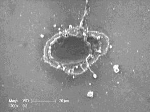
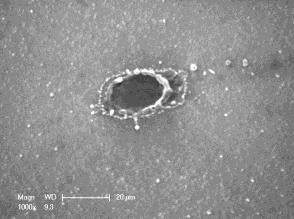
80 Current (A) Current (A) Current (A) Current (A) Current (A) Current (A) Current (A) µj/pulse 190 µj/pulse 138 µj/pulse 146 µj/ pulse 119 µj/pulse 87 µj/pulse 35 µj/pulse 20 µm 1.E-03 1.E-06 1.E-09 1.E-12 1.E-03 1.E-06 1.E-09 1.E-12 1.E-03 1.E-06 1.E-09 1.E-12 1.E-03 1.E-06 1.E-09 1.E-12 1.E-03 1.E-06 1.E-09 1.E-12 1.E-03 1.E-06 1.E-09 1.E-12 1.E-03 1.E-06 1.E-09 1.E Voltage (V) Voltage (V) Voltage (V) Voltage (V) Voltage (V) Voltage (V) Voltage (V) Figure 3-19: SEM images and I-V measurements of LDEs on a-si:h/n+ a-si:h sample, 1064 nm laser.
81 66 Images and I-V curves for the a-si:h/n+ a-si:h/sio x sample are shown in Figure The leakage current is reduced in these LDEs due to the SiO x layer, and in several cases forward bias current is reduced as well and series resistance dominates the measurement. There are a few conditions that hold promise for manufacturing LDEs in cells, and they will be investigated further in the next section. Notably those processing conditions of interest are the lower energy pulses.
 Current (A) 67 285 µj/pulse 190")


 Figure 3-20: SEM images and I-V")

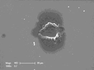
82 Current (A) Current (A) Current (A) Current (A) Current (A) Current (A) µj/pulse 190 µj/pulse 138 µj/pulse 146 µj/ pulse 119 µj/pulse 87 µj/pulse 20 µm 1.E-03 1.E-06 1.E-09 1.E Voltage (V) 1.E-03 1.E-06 1.E-09 1.E Voltage (V) 1.E-03 1.E-06 1.E-09 1.E Voltage (V) 1.E-03 1.E-06 1.E-09 1.E Voltage (V) 1.E-03 1.E-06 1.E-09 1.E Voltage (V) 1.E-03 1.E-06 1.E-09 1.E Voltage (V) Figure 3-20: SEM images and I-V measurements of LDEs on a-si:h/n+ a-si:h/sio x sample, 1064 nm laser.
83 68 Curve Comparison Further comparison of the specific I-V curves selected earlier provided insight into suitable LDE laser processing conditions. I-V measurements do not give a comprehensive picture of device performance and only with the evaluation of parameters in a diagnostic cell can we fully evaluate all the factors that contribute to performance in a cell. While the I-V measurements may not be characteristic of each LDE created with certain laser processing conditions, in our preliminary investigation it is useful to compare the I-V measurements and determine the laser processing conditions that yielded LDEs with the best diode characteristics. Comparing the previously selected curves together, only those with the best turn on characteristics were selected for further examination. As shown in Table 3-2, the 1070 nm and 1064 nm lasers were useful in the formation of a majority of these LDEs. Those selected are shown in an I-V plot, and additionally shown on a log(i)-v plot in Figure Markers have been added to indicate slopes with ideality factors equal to 1 and 2 on the log(i)-v plot. Featuring low series resistance and leakage currents on the order of 1x10⁻⁸ A, the a- Si:H/n+a-Si:H structure yielded LDEs for a majority of the laser processing conditions to which it was exposed. The LDEs formed on the a-si:h/sio x passivation structure were formed with fewer processing conditions; however, those that were fabricated had the lowest leakage currents observed, on the order of 1x10-11 A. LDEs were more difficult to fabricate on the a-si:h/n+asi:h/sio x sample as compared to the a-si:h/n+a-si:h sample because of the laser interaction with the robust SiO x layer in the former.
84 69 Table 3-2: LDE parameters plotted in Figure Laser LDE Parameter Passivation Fluence 1064 nm 35 µj/pulse a-si:h 11.1 J/ cm nm 119 µj/pulse a-si:h 37.9 J/ cm nm 146 µj/pulse a-si:h 46.5 J/ cm nm 190 µj/pulse a-si:h 60.5 J/ cm nm 100 W, 250 µs a-si:h 31.8kJ/ cm nm 77 W, 250 µs a-si:h 24.3 kj/ cm nm 67 W, 300µs a-si:h 25.6 kj/ cm nm 100 W, 100 µs a-si:h/sio x 12.7 kj/ cm nm µj/pulse (3 pulses) a-si:h 57.7 J/ cm nm µj/pulse (2 pulses) a-si:h J/cm 2 Note: a-si:h represents 10 nm a-si:h/ 100 nm n+ a-si:h passivation and a-si:h/sio x represents 10 nm a-si:h/ 20 nm n+ a-si:h/ 100 nm SiO x passivation
 38 J/cm2 1064 nm (a-si:h) 47 J/cm2 1064 nm (a-si:h) 61 J/cm2 1064 nm (a-si:h) 32 kj/cm2 1070 nm (a-si:h) 24 kj/cm2 1070 nm (a-si:h) 26 kj/cm2 1070 nm (a-si:h) 13")
85 Current (A) Current (A) E E E E E E E E E J/cm nm (a-si:h) 38 J/cm nm (a-si:h) 47 J/cm nm (a-si:h) 61 J/cm nm (a-si:h) 32 kj/cm nm (a-si:h) 24 kj/cm nm (a-si:h) 26 kj/cm nm (a-si:h) 13 kj/cm nm (a-si/siox) 53 J/cm2 355 nm (a-si:h) 35 J/cm2 355 nm (a-si:h) Voltage (V) 11 J/cm nm (a-si:h) n=2 1.0E E E-04 n=1 1.0E E E E J/cm nm (a-si:h) 47 J/cm nm (a-si:h) 61 J/cm nm (a-si:h) 32 kj/cm nm (a-si:h) 24 kj/cm nm (a-si:h) 26 kj/cm nm (a-si:h) 13 kj/cm nm (a-si/siox) 53 J/cm2 355 nm (a-si:h) 35 J/cm2 355 nm (a-si:h) 1.0E E E E E Voltage (V) Figure 3-21: I-V and log(i)-v plots of the best diode characteristics.
86 71 Examining the curves in Figure 3-21, the LDE processed at 47 J/cm 2 on the a-si:h passivation layer with 1064 nm laser, and the LDE processed at 13 kj/cm 2 on the dual stack passivation layer with the 1070 nm laser, achieved the largest currents at forward bias. Looking at the log (I)-V plot it appears that the series resistance of each of the LDEs selected is approximately the same; however, the ideality factors and saturation and leakage currents vary greatly. Most of the LDEs have ideality factors (η qnr ) somewhere between 1 and 2. Given the wide range of fluences used across each laser to produce functional LDEs one would not expect each LDE s I-V characteristics to be similar. To more closely evaluate the diode characteristics of each, fitting of the measured I-V curves was performed by manipulating values for I o,scr, I o,qnr, n scr, n qnr and r s in Equation 1, the equation for current in a diode. The majority of the I-V curves on the log(i)-v plot are very dissimilar, due to varying fluences, pulse durations, and wavelengths used to create them. Two particular LDEs formed with 1070 nm laser feature similar fluences and are of interest to compare. Both LDEs were created with fluences of ~25kJ/cm 2 on the a-si:h/n+a-si:h passivation structure. Shown in Figure 3-22, the I-V measurements of the LDEs, processed at 77 W and 250 µs and 67 W and 300 µs are very similar. The LDE processed with 77 W and 250 µs had a leakage of 8.2x10⁻⁸ A, a saturation current of 3.0x10⁻¹¹ A, a series resistance of 90 Ω, and an ideality factor of 1.6. The LDE processed with 67 W and 300µs had a leakage of 8.2x10⁻⁸ A, a saturation current of 7.0x10⁻¹¹ A, a series resistance of 100 Ω, and an ideality factor of 1.7.
87 Current (A) 72 1.E-01 1.E-02 1.E-03 n=1 1.E kj/cm2, 77 W 250 µs 1.E kj/cm2, 67 W 300 µs 1.E-06 n=2 1.E-07 1.E-08 1.E-09 1.E-10 1.E-11 1.E Voltage (V) Figure 3-22: Curves for similar LDEs. One curve in particular, measured for the LDE processed with the 1070 nm laser at 100 W and 100 µs on the P doped a-si:h/n+ a-si:h/sio x structure, showed the best I-V characteristics. It exhibited a very low leakage current of 1.1x10⁻¹¹ A, a saturation current of 6x10-13 A, a series resistance of 100 Ω, and an ideality factor of 1.3 (the closest to 1 out of all measurements). Given that the diameter of the LDE is approximately 20 µm, the leakage current density is approximately 3.5x10⁻⁶ A/cm 2. The saturation current density is approximately 2x10⁻⁷ A/cm 2 (or approximately 4x10⁻⁸ A/cm 2 considering the junction area revealed in cross section). This value is large compared to reports of 8.5x10⁻¹³ A/cm 2 for laser chemically processed emitters (11) and 8.8x10⁻¹⁴ A/cm 2, which is the lowest theoretical saturation current density for an LDE (6). The fluence calculated for the creation of this LDE was 12.7 kj/cm 2, again a large value compared to those reported in literature ( J/cm 2 ). From these evaluations the emitters fabricated are not of a quality that would lend them to use in solar cell manufacturing. While we were able to demonstrate laser doping, the
88 73 saturation (2x10⁻⁷ A/cm 2 ) and leakage currents (3.5x10⁻⁶ A/cm 2 ) of our LDEs were much higher than those in the literature (11). Future experiments will seek to further understand the formation of laser doped emitters and the critical aspects of their laser processing. One place to start is with the reduction of laser fluences used in LDE formation. Compared to those reported in the literature the values utilized herein are exceedingly large. The thickness of the passivation/dopant structures necessitated the large energies that we used, and in the future passivation and doping layers that are better suited to gentler laser fluences must be fabricated. Thinner layers should make the use of less energy possible. Once appropriate passivation/dopant structures are developed, in conjunction with milder laser processing parameters, better quality LDEs should be attainable. Processing improvements will lead to reduced laser damage and carrier recombination, easily observed in I- V measurements by lower saturation currents, minimal leakage current, and ideality factors closer to 1. In the future, diagnostic cells will also be used to understand the impact of emitter performance on the overall cell. Of the lasers examined, the 1070 nm and 1064 nm lasers were used with numerous processing conditions to create LDEs. The 355 nm laser exhibited ablation when forming LDEs and may not be suitable for further investigation if thinner dopant/passivation structures are used. Metallization In an attempt to conclusively measure I-V curves for each LDE without uncertainty in the measurements, metallization of the contacts became an additional area of experimentation. Due to the large radius of the probe tip in comparison to the LDE diameter, and the surface topography of each laser processed region, exact placement of the probe on a specific area of the LDE was very difficult, as pictured in Figure Metalizing the LDE sample would allow for


89 uniform contact to the device with only a minimal addition of contact resistance, assuming an ohmic metal contact could be made to the top surface of the rectifying LDE. 74 Figure 3-23: Possible locations of probe tip contacting the LDE when taking I-V measurements. When considering the passivation structures in our experiments it is important to note that depositing metal onto an a-si:h film would effectively short out measurement of the LDE. It is critical that there be an insulating layer between the metal film and the underlying passivation stacks so that only the I-V characteristics of the LDE are measured. On samples with the SiO x overlayer contact would be made only to the LDE. Figure 3-24 highlights the problem for the case the case of nickel deposition and silicide formation. Figure 3-24: Importance of a SiO x barrier layer for selective metallization of LDEs.
90 Blanket metallization poses an additional problem in that each LDE will be contacted and any measurements would represent the current contributions of all of the LDEs rather than just 75 one. Selective or patterned metallization would be required to measure accurately the I-V characteristics of only one LDE, ensuring that only the laser doped region was metallized. The first approach taken to metallize the samples was to pattern and e-beam deposit nickel over each pad, understanding that e-beam deposition would contact all the LDEs in each array and I-V measurements would include their contributions. Only samples with a SiO x layer were used to ensure contact to only the LDEs. Prior to deposition the samples were etched in a dilute solution of 50:50 DI water to buffered oxide etch (1:10 BOE). Etching was very brief (3 to 6 s) to ensure that the passivation oxide was not removed entirely. Nickel was deposited to a thickness of 150 nm in an Axxis e-beam deposition system. Liftoff was performed using Microchem Remover PG and samples were then annealed at 450 C in an RTA for 15 min in an attempt to form NiSi. After annealing it became apparent that tensile stresses existed in the deposited Ni film. Shown in Figure 3-25, cracking and peeling of the film occurred on several of the metallized pads. E-beam deposition has been known to introduce stresses in metal films as they are deposited, but another likely cause of the stress was the excessive thickness of the metal layer, 150 nm. In the future, sputter deposition would allow for control of stresses in the metal film through the manipulation of chamber pressure, and a thinner film may be used. Lessons from this first metallization attempt gave insight into what needs to occur in future work.

91 76 1 mm Figure 3-25: Tensile stresses evidenced in Ni films by peeling. I-V measurements were taken on the sample to study the changes in the curves due to blanket metallization. The probe tip was placed in various locations on the metal pad to ensure that probe location did not impact the current measurement. The probe was placed on the metal pad (offset from the LDE) and directly on a metallized LDE. The curves acquired in both sweeps were the same, indicating that metallization removed measurement variability due to probe placement. When comparing the I-V curves taken before on the bare LDE with those taken after metallization, it became clear that the magnitude of current measured had increased. The increase in current was expected since a single LDE was no longer being measured, but all nine. The current increase is not a sum of each diodes individual contribution and cannot be directly predicted; the most conductive diode will dominate the measurement with additional contribution

92 Current (A) from the other LDEs. Figure 3-26 highlights the current increase in the post metallization measurement. 77 1x10 1.0E x10 1.0E E-06 1x E-08 1x E-10 1x10 Post Metallization on LFE Post Metallization on Metal Pre Metallization 1.0E-12 1x Voltage (V) Figure 3-26: Pre and post metallization I-V measurements on a pad processed with the 355 nm laser (155 µj). Cross-sectioning and Junction Delineation To determine LDE depth within the substrate cross-sectioning was employed. Dense arrays of LDEs were created with select processing conditions drawn from I-V measurement results. The process used herein was identical to the procedure used for LFC cross-sectioning and junction delineation, but the sample structure is different. The wafer substrate for these samples was p-type, so that laser doping of the n-type emitter would be highlighted. Plating should occur on the laser doped region rather than the substrate. For the 1070 nm laser the first LDE sample analyzed was created with processing conditions of 100 W and 100µs on the a-si:h/n+ a-si:h substrate. The dense array prior to sample preparation and the subsequently polished and plated cross-section are shown in Figure 3-27.


93 78 Diameter = 47 µm Diameter = 47 µm 10 µm Figure 3-27: Dense array of LDEs processed at 100W and 100 µs on a-si:h/n+ a-si:h sample using a 1070 nm laser. Initial assessment of the LDE cross-section shows that the doped emitters are much shallower than the LFCs fired with the 1070 nm laser, with depths of 11 µm. Pulse durations for the LDEs are much shorter than those used to fire LFCs, although the powers are comparable. The short duration of the laser pulse and the different wafer structure used to dope LDEs result in the large difference in geometry and aspect ratio. The approximate width of the LDEs processed at 100 W and 100 µs was 45 nm, and the approximate penetration depth was 11 nm. Width = µm Depth = µm 20µm 20µm Figure 3-28: Cross-section of LDEs processed with a 1070 nm laser at 100 W and 100 µs.


94 79 Cross-sectioning was attempted on a sample processed with the 355 nm laser with 1 pulse at µj. The 355 nm wavelength of the laser is strongly absorbed in the very near surface of the sample; with only a 30 ns pulse duration there is not a deeply doped region apparent. From the cross-sectioning and plating of this sample it was confirmed that the doping occurs in only a very shallow region. Further samples with different processing conditions will be examined in future work. Images of the cross section attempt for the single µj pulse sample are show in Figure Diameter = 51 µm 20µm 10µm Figure 3-29: Cross-sectioned LDE sample processed with 1 pulse at µj/pulse with the 355 nm laser. Results and Discussion Through SEM investigation and I-V measurements it was quickly determined that the Sb dopant structure on both the a-si:h and a-si:h/sio x passivated samples was not a robust structure suitable for laser doping a selective emitter. Delamination and peeling of the e-beamed evaporated Si/Sb/Si structures occurred prior to laser firing, and when processed with each laser further delamination and volatilization occurred. Diodes were only formed on Sb samples processed with the 355 nm laser, but the I-V characteristics and excessive delamination apparent did not make them suitable for further investigation.
95 80 Diodes were formed, using each laser, on both of the P doped a-si:h/n+ a-si-h and a- Si:H/n+ a-si:h/sio x passivated sample structures. LDEs processed with the 1070 nm and 1064 nm lasers exhibited the least ablation, whereas the 355 nm laser caused ablation across all the LDEs created with it. In I-V measurements it was clear for LDEs processed with the 355 nm laser on the a-si:h/n+ a-si:h/sio x passivated sample it was difficult to form diodes with low series resistance. Ablation of the thin dopant layer with the passivation stack likely led to less doping of the P within the substrate. LDEs processed with the 1070 nm, µs laser exhibited low series resistance, but were formed only when shot with the highest powers and longest durations. At lower power and pulse duration no change to the substrate was apparent. Leakage currents of LDEs created with the 1070 nm laser were lower on the a-si:h/n+ a-si:h/sio x passivated sample than those created on the a-si:h/n+ a-si-h passivated sample. The insulating SiO x layer limits current transport to only the LDE and any parallel paths that would be possible through the a- Si:H/n+ a-si-h layer are blocked. LDEs doped using the 1064 nm laser showed similar I-V characteristics to those doped with the 1070 nm laser but exhibited larger diameters and some ablation. Leakage currents were lower on the a-si:h/n+ a-si:h/sio x passivated sample than those created on the a-si:h/n+ a-si-h passivated sample, and also the LDEs created on the Si:H/SiO x passivated sample were slightly smaller and showed less ablation splatter. The fluences used to fabricate LDEs were much larger than those in the literature; values of 10s of J/cm 2 were reached for the 1064 nm and 355 nm lasers, and values of 10s of kj/cm 2 were reached for the 1070 nm laser (under 1.0 J/cm 2 used in (11)). Only because of the robustness of the passivation and dopant stack layers were such large values required. A much thinner structure would require lower fluences. The leakage and saturation current of those LDEs selected for further investigation were much higher than those reported in the literature. Ideality values ranged between 1 and 2, with the best estimated to be 1.3 for the LDE doped with the 1070 nm laser with 100 W and 100 µs on
96 81 the P doped a-si:h/n+ a-si:h/sio x structure. The leakage current of that sample was of 1.1x10⁻¹¹ A, and the saturation current was of 6x10-13 A. The resulting saturation current density was approximately 2x10⁻⁷ A/cm 2 (or approximately 4x10⁻⁸ A/cm 2 considering the junction area revealed in cross section). Series resistance in most of the select LDEs was less than 200 Ω. E-beam deposition of Ni to form nickel silicide was possible, but several difficulties were encountered during processing. Blanket metallization eliminated the ability to selectively measure just one LDE. Additionally, e-beam evaporation of Ni to the thickness of 150 nm caused excessive stress in the films, and upon annealing they peeled and delaminated due to the tensile forces within them. It was clear that a thin oxide barrier layer would be necessary to metallize the samples to ensure measurement of only the LDEs and eliminate other possible current paths. Future work will include sputter deposition of a thinner Ni film onto a passivation structure capped with a SiO x film. Cross-sectioning and junction delineation was again used to identify the regions where doping had occurred beneath the laser processed regions. The n-type doped regions were selectively plated and dimensions of the depth and width of the LDEs were obtained. For those LDEs processed at 100 W and 100 µs with the 1070 nm laser, their penetration depth was ~11 nm and their width was ~45 nm. The sample cross-sectioned for the 355 nm laser showed some plated regions; however, they were not definitive enough to determine the maximum width or depth. Additional samples will be cross-sectioned in the future to better correlate dopant depth and penetration to laser processing parameters. In summary, LDEs have been fabricated, and a particular dopant and passivation structure was identified for future experimentation. LDEs were created on the P doped n+ a-si:h samples with each laser, while the Sb doped samples were not resilient enough to withstand laser firing with the longer wavelength lasers and LDEs were not measureable. It should be possible to fabricate LDEs suitable for a solar cell with further refinement of processing parameters and
97 passivation layer thicknesses. Evaluation of diagnostic cells will also be possible with the development of a more robust metallization technique. 82
98 83 Chapter 4 Passivation Literature Review Recent investigations into surface passivation have highlighted aluminum oxide (Al 2 O 3 ) as a promising alternative to conventional passivation layers used in solar cell manufacturing. Unlike hydrogenated amorphous silicon (a-si:h), silicon nitride (SiN x ) and silicon oxide (SiO 2 or SiO x ) layers, which create surface passivation through the reduction of dangling bonds, Al 2 O 3 and similar metal oxides afford fixed charge passivation, which reduces recombination at the surface through field effects. On an n-type wafer, sufficient negative fixed charge creates an inversion layer and shields majority carriers from the surface; on a p-type wafer negative fixed charge creates an accumulation layer and shields minority carriers from the surface, thus preventing their recombination at surface states (18). Fixed charge passivation is very robust both thermally and under light soak, making it advantageous over passivation achieved with a-si:h layers, which degrade over time due to the loss of hydrogen in the film at moderate temperatures (greater than ~150 C) (52) (53). Rather than a physical means of dangling bond passivation to reduce surface recombination, Al 2 O 3 provides field effect passivation to force electrons away from the surface and prevent recombination. Hydrogenated amorphous silicon and SiO x layers are commonly deposited using PECVD and can be deposited quickly on large areas. Hydrogenated amorphous silicon can be grown at low temperatures, around 150 C, and can provide passivation with a low surface recombination velocity on the order of 10 cm/s (53). Unfortunately, the passivation provided by the film degrades when exposed to higher temperatures and over time, due to loss of hydrogen from the
99 84 film (53). Thermally growing silicon oxide, SiO 2, provides a more robust, chemically inert passivation, which can result in long effective carrier lifetimes, in the ms range, and low SRVs, from 1 to 40 cm/s depending on the wafer type (54). Thermal oxidation, however, requires exposing silicon to high temperatures around 1000 C (19) (54). Aluminum oxide and hafnium oxide (HfO 2 ), investigated herein for fixed charge passivation, are typically deposited using atomic layer deposition (ALD) at low temperatures in the range of 100 to 200 C (19). Record SRVs achieved for Al 2 O 3 have been as low as 3 cm/s (15). Atomic layer deposition relies on specific gaseous precursors, which complete selflimiting reactions, to form the desired metal oxide (55). The precursors are introduced in alternating pulses into a low pressure reaction chamber to grow one layer of the reaction product at a time; one pulse of each precursor completes one cycle. For the growth of Al 2 O 3, typical precursors are trimethylaluminum (Al(CH 3 ) 3 ) and water vapor (H 2 O) (55). Oxygen plasma in plasma assisted ALD, or ozone, can also be used with Al(CH 3 ) 3 (18) (19) (20). The reactions that take place during each pulse are as shown below (55). Hydrogen terminated bonds at the silicon surface are required to start the reaction, which then proceeds one layer at a time with each cycle. Si-O-H (s) +Al(CH 3 ) 3(g) :Si-O-Al(CH 3 ) 2(s) + CH 4(g) :Si-O-Al(CH 3 ) 2(s) + 2 H 2 O (g) :Si-O-Al(OH) 2(s) + 2 CH 4(g) Several groups have demonstrated excellent passivation of silicon using ALD Al 2 O 3 and stacked structures of Al 2 O 3 and another dielectric. Schmidt et al. investigated both Al 2 O 3 and Al 2 O 3 /SiO x passivation layers for rear side passivation of a p-type PERC cell (19). Efficiencies of 20.0% and 20.6% were confirmed for 130 nm ALD Al 2 O 3 and 30 nm ALD Al 2 O 3 /200 nm PECVD SiO x rear passivation stacks, respectively. The rear side contacts were made through standard photolithographic patterning and etching steps. After contact formation the entire cell was subjected to a 10 min 500 C front oxidation step and a final 1 min 300 C anneal (19). Surface recombination velocities of cm/s and cm/s were measured for the 130 nm
100 85 alumina layer and the 30 nm Al 2 O 3 /200 nm SiO x layers, respectively (19). Benick et al. fabricated n-type PERL solar cells with efficiencies of % using Al 2 O 3 for front surface passivation of the highly doped p-type emitter (56). A 30 nm Al 2 O 3 front surface passivation layer was deposited by plasma-assisted ALD followed by plasma-assisted CVD of a 40 nm SiN x ARC. The best efficiency achieved was 23.2% (56). Suwito et al. fabricated a similar PERL-like cell, with a 10nm Al 2 O 3 front side passivation layer and SiN x anti-reflection coating, and achieved an efficiency of 22.4% (16). Saint-Cast et al. demonstrated solar cells with efficiencies ranging from 21.2 to 21.5% passivated with both Al 2 O 3 and Al 2 O 3 /SiO x layers. Al 2 O 3 layers were depositing using both ALD and PECVD (20). Stacked passivation layers studied included 7 nm ALD Al 2 O 3 /90 nm PECVD SiO x, 20 nm ALD Al 2 O 3 /80 nm PECVD SiO x, and 30 nm PECVD AlO x /70 nm PECVD SiO x ; however, a sample passivated with 100 nm PECVD AlO x cell exhibited the highest efficiency of 21.5% and lowest SRV of 8 cm/s. Across the different passivation structures, surface recombination velocities ranged from approximately 8 to 108 cm/s. From their findings the authors concluded that Al 2 O 3 passivation layers were comparable to a-si:h and SiO 2 for solar cell passivation, becoming the third suitable material for use in manufacturing (20). Hoex et al., in a study on Al 2 O 3 passivation of p-type silicon, attributed the excellent passivation of Al 2 O 3 to a large negative fixed charge density that repelled minority carriers (electrons in a p-type material) away from the surface, thereby reducing the recombination rate of carriers at the surface (18). They claimed a fixed charge density of 1x10 13 q/cm 2 in a 30 nm Al 2 O 3 plasma-ald film after a 30 min 425 C anneal in a N 2 ambient. The SRVs reported were measured for Al 2 O 3 passivated samples, in comparison with samples passivated with SiO 2, a-si:h and a-sin x :H films. Surface recombination velocities were calculated based on the effective carrier and bulk carrier lifetimes of each sample, and were reported to be in the range of ~ cm/s for the Al 2 O 3 films (18). In other work by Hoex et al. SRVs of 2 cm/s and 13 cm/s were
101 86 obtained on n- and p-type silicon wafers passivated with 7 to 30 nm Al 2 O 3 films, annealed at 425 C in a N 2 ambient in a rapid thermal annealing (RTA) furnace (15). Even layers as thin as 7 nm were reported to exhibit SRVs as low as 5 cm/s on n-type silicon. Effective carrier lifetimes as high as 1.2 ms were measured on p-type silicon passivated with 30 nm Al 2 O 3, and a maximum lifetime of 6.6 ms was measured on n-type silicon passivated with 26 nm Al 2 O 3, although negative fixed charge is not the mechanism by which n-type silicon is passivated, as it would create an inversion layer. Hoex et al. claimed that such values were comparable to the longest lifetimes obtained for alnealed SiO 2, a-sin x :H, as well as a-si:h films typically used in solar cell passivation (15). ( Alnealing involves annealing a passivation layer after having deposited an Al film on top prior to heat treatment. After the annealed Al film is removed, there is a noted improvement of the passivation quality of the silicon derivative films (19).) Hoex et al. attribute the high lifetimes and low SRVs obtained with the Al 2 O 3 passivation films to a built-in, negative, fixed charge density of ~10 13 cm -2, responsible for inducing field effect passivation in the p-type samples (15). The large negative fixed charge density was calculated from flat band voltage shifts seen in C-V measurements, which they did not report. Benick et al. examined the thermal stability of Al 2 O 3 on p-type silicon. Two sets of samples were passivated with 27 nm of plasma-assisted ALD Al 2 O 3 on 0.1, 0.5, and 1.0 Ω-cm FZ p-type silicon. One set was deposited at 170 C, and the other at 230 C. After deposition, individual samples were cleaved in order to receive different annealing treatments. Anneals were performed in forming gas at either 440 C or 500 C (52). A maximum lifetime of 3.3 ms was achieved on the 1.0 Ω-cm sample annealed at 440 C in forming gas. Samples were additionally subjected to temperatures up to 850 C for 3 seconds, and while some degradation occurred, passivation quality was still high (52). In an additional study by Schmidt et al., thinner Al 2 O 3 layers were studied for passivation integrity and robustness when subjected to high temperatures (57). After annealing at 425 C in for 15 min, they measured a lifetime of 550 µs (22 cm/s) for a
102 nm film, and a lifetime of 1 ms for a 20 nm film on a 1.5 Ω-cm wafer. Similarly, they achieved lifetimes of 8 ms (1.8 cm/s) for a 3.6 nm film, and 10 ms (1.4 cm/s) for a 20 nm film on 200 Ω-cm wafers. However, after firing at 830 C the passivation degraded, and in the case of the ultra thin 3.6 nm Al 2 O 3 layer the lifetime was reduced to 50 µs. Thermal stability of thin Al 2 O 3 passivation layers was improved with the deposition of a PECVD SiN x capping layer (57). The initial lifetime of a 3.6 nm Al 2 O 3 /75 nm SiN x sample was 700 µs before firing and dropped less severely to 300 µs after firing. Maintaining passivation of the substrate after firing was attributed to the deposition of the SiN x layer and the hydrogen it introduced. The authors claim that hydrogen present in the SiN x provided passivation by diffusing to the Al 2 O 3 /Si interface where it satisfied dangling bonds. Little investigation into HfO 2 as a passivation layer for silicon has been performed. One report by Wang et al. found that HfO 2 provided negative fixed charge passivation similar to Al 2 O 3 (58). They deposited Al 2 O 3 and HfO 2 films on two n-type silicon samples using ALD for 150 cycles at 200 C. No additional annealing was performed. By studying C-V characteristics and V FB shifts they found negative fixed charge in the bulk of the films. They measured as deposited effective carrier lifetimes of 302 µs and 347 µs for the Al 2 O 3 and HfO 2 passivated samples, using µ-pcd. The lifetime values correlated to maximum SRVs of 84.5 cm/s and 73.4 cm/s, respectively (58). Interestingly, they report that for each dielectric an increase in the film thickness leads to lower SRVs. For use in solar cells, ALD and PECVD deposited Al 2 O 3 hold much promise as a passivation layer that could surpass the long term integrity and robustness of a-si:h and SiO x films. Many groups have demonstrated its capabilities in test cells but little work has been done to understand in detail the fixed charge passivation and how to optimize it. An investigation of the factors that contribute to fixed charge passivation is performed herein to determine the best material systems and layers for cell passivation. Both Al 2 O 3 and HfO 2 are considered. The work


103 88 herein attempts to determine the effect of film thickness, annealing treatments, fixed charge density, SiO x capping layers, and multi-layers structures on passivation quality. Passivation was evaluated through effective carrier lifetime measurements, C-V measurements, fixed charge density calculations, and sheet resistance measurements. Single layer films of Al 2 O 3 are studied in conjunction with Al 2 O 3 /SiO x layered films to better understand the passivation mechanisms of each. Passivation Experiments A series of experiments were designed to study performance of Al 2 O 3 and HfO 2 layers, Al 2 O 3 /SiO x and HfO 2 /SiO x layers on the passivation of crystalline silicon wafers, and to investigate the potential of fixed charge passivation for use in high efficiency solar cells. On an n-type wafer, sufficient negative fixed charge creates an inversion layer thus shielding majority carriers from the surface; on a p-type wafer, negative fixed charge creates an accumulation layer thus shielding minority carriers from the surface. In either case, the presence of fixed charge in the passivation layer serves to shield one type of carrier from the surface of the silicon, thereby providing passivation and reducing surface recombination.
104 Figure 4-1: Cambridge Savannah TM 200 ALD system and the AMAT P-5000 cluster tool. 89 Alumina (Al 2 O 3 ) and hafnia (HfO 2 ) layers were deposited using atomic layer deposition (ALD) in a Cambridge Savannah 200 system shown in Figure 4-1. In later experiments SiO x capping layers were deposited using an Applied Materials P-5000 four chamber cluster tool. While ALD has often been ignored as a large scale production tool, progress is being made to increase the rate and scale of ALD by developing a spatial technique to separate deposition steps (59). In conventional ALD the cycle time remains a limiting factor; however, thin films (< 10 nm) can be deposited rapidly, and would suffice as long as a thinner film is adequate for passivation. Additionally, passivation layers similar to those grown by ALD can be deposited in PECVD systems, and although we did not have the capability to compare PECVD and ALD films directly, other groups have found passivation quality of the films to be similar (20). Three sets of experiments were performed. The first investigated the passivation of silicon by layers of Al 2 O 3 and HfO 2 with increasing thicknesses from 4 nm to 35 nm, and is presented in the section Film Thickness Experiment: Al 2 O 3 and HfO 2 Layers. The second compared passivation by single Al 2 O 3 layers to that of Al 2 O 3 capped with SiO x layers, and is presented in the section Multi-Layer Passivation Experiment: Al 2 O 3 /SiO x and HfO 2 /SiO x Layers. The third was an investigation into maximizing fixed charge density in Al 2 O 3 and Al 2 O 3 /SiO x layers with the goal of creating an induced inversion layer in a highly resistive test silicon substrate, and is presented in the section Inversion Layer Experiment: Al 2 O 3 and Al 2 O 3 /SiO x Layers.
105 90 Film Thickness Experiment: Al 2 O 3 and HfO 2 Layers The first experiment carried out was designed to correlate the passivation of silicon by ALD films of Al 2 O 3 and HfO 2 with different film thicknesses and annealing treatments. Effective carrier lifetime measurements and C-V measurements were used to evaluate the changes in surface passivation and determine the presence and quantity of fixed charge in the passivation layers. Two sets of samples were created, the first passivated with Al 2 O 3 films with thicknesses of 8, 12, 20, and 35 nm, and the second passivated with HfO 2 films with thicknesses of 9, 13, 22, and 38 nm. The films were deposited in the Cambridge ALD tool at 200 C. For the deposition of Al 2 O 3, the first precursor, water, was pulsed for s followed by a wait time of 8 s, after which the trimethylaluminum precursor was pulsed for s followed by an 8 s wait time. Deposition and run time details are given Tables 4-1 and 4-2 for each film deposited. Table 4-1: Al 2 O 3 deposition details. Al 2 O 3 Sample Cycles Film Thickness Deposition Temperature Deposition Time A nm 200 C 22 min A nm 200 C 33 min A nm 200 C 54 min A nm 200 C 98 min Table 4-2: HfO 2 deposition details. HfO 2 Sample Cycles Film Thickness Deposition Temperature Deposition Time H nm 200 C 32 min H nm 200 C 45 min H nm 200 C 69 min H nm 200 C 122 min


106 91 Thicker films take much longer to deposit given the increased number of cycles required. Despite any superior passivation quality potentially achieved with a 35 nm film, a deposition time of 98 min may not be realistic in a manufacturing setting. Other groups, however, have demonstrated high-efficiency solar cells passivated with similar thickness Al 2 O 3 layers, warranting the comparison. After deposition, two different annealing treatments were performed to improve the films and drive out organics or impurities. The first anneal was carried out at 250 C for 5 min on a Temptronic vacuum chuck, and the second at 350 C for 5 min on a Thermolyne hot plate, both shown in Figure 4-2. Annealing temperatures were confirmed with a thermocouple during heat treatment, and were performed in ambient air. Figure 4-2: Barnstead Thermolyne hot plate and Temptronic ThermoChuck vacuum chuck. Lifetime Measurements Effective carrier lifetime was measured for each sample before and after annealing treatments to observe any change in minority carrier lifetime and determine any improvement in surface passivation. Measurements were performed using a microwave photoconductive decay (µ-pcd) tool built in house. A description of the measurement process can be found in Appendix
107 92 A. A microwave antenna was used to transmit microwaves to the sample and then measure the reflected microwave power from the sample, while the sample was illuminated on the opposite side with a UV LED. The UV wavelength excited carriers (electron-hole pairs) within the bulk of the silicon and near the surface. Once excited the carriers exist for a characteristic time before they recombine. That time is the effective carrier lifetime, and can be prolonged by adequate surface passivation. Longer effective carrier lifetimes indicate better passivation and reduced carrier recombination at the surface. The length of the carrier lifetime can be extrapolated from the decay of microwave power captured by the antenna, since photoconductivity and reflectivity are linked. An example of a reflected power curve measured on an annealed sample (P- A10S100-4_450a_RTA) and the µ-pcd set up used is shown in Figure 4-3.

108 Reflected Power (mw) mw = τ = 1040 µs Time (s) Figure 4-3: Microwave photoconductive decay, effective carrier lifetime measurement set up (50). Average effective carrier lifetime values for the Al 2 O 3 and HfO 2 passivated samples are shown in Table 4-3 and Table 4-4. Measurements were taken as deposited, after a 5 min 250 C anneal, and after a 5 min 350 C anneal.
109 94 Table 4-3: Effective carrier lifetime for Al 2 O 3 passivated samples. Al 2 O 3 Sample Film Thickness As Deposited Post 250 C Post 350 C A1 8 nm 370 µs 312 µs 1012 µs A2 12 nm 420 µs 618 µs 1030 µs A3 20 nm 510 µs 817 µs 1722 µs A4 35 nm 594 µs 480 µs 440 µs Table 4-4: Effective carrier lifetime for HfO 2 passivated samples. HfO 2 Sample Film Thickness As Deposited Post 250 C Post 350 C H1 9 nm 365 µs 765 µs 859 µs H2 13 nm 356 µs 775 µs 1070 µs H3 22 nm 480 µs 793 µs 760 µs H4 38 nm 656 µs 1063 µs 296 µs Effective carrier lifetimes for samples passivated with both the Al 2 O 3 and HfO 2 films, as deposited, appear to increase with increasing film thickness. Certain samples exhibited a trend of increased effective carrier lifetime with increased annealing temperature, highlighted in Figure 4-4, particularly the 12 nm and 20 nm Al 2 O 3 passivated samples, and the 9 nm and 13 nm HfO 2 passivated samples. The 5 min 350 C hot plate anneal was more effective than the 250 C vacuum chuck anneal for these samples, and this treatment sufficiently activated the fixed charge in the film leading to increased effective carrier lifetimes and reduced surface recombination. Samples passivated with the thinner films exhibited very long lifetimes, greater than 1 ms for the sample passivated with the thinnest 8 nm Al 2 O 3 film, and up to 1.7 ms for the sample passivated with 20 nm Al 2 O 3 sample. It is interesting to note, however, that samples passivated with the thickest Al 2 O 3 and HfO 2 films did not improve with the 5 min 350 C anneal.
 Annealing Temperature ( C) Figure 4-4: Effective carrier lifetime and annealing temperature.")

110 Lifetime (µs) Lifetime (µs) Al 2 O 3 Films 8nm film 12nm film 20nm film 35nm film HfO 2 Films 9nm film 13nm film 22nm film 38nm film Annealing Temperature ( C) Annealing Temperature ( C) Figure 4-4: Effective carrier lifetime and annealing temperature. C-V Measurements Capacitance-voltage (C-V) measurements were performed to determine the fixed charge densities of the passivation films before and after each annealing treatment. A Leighton 2017B mercury probe, shown in Figure 4-5, was used with an Agilent 4284A LCR meter to measure capacitance while applying a DC voltage sweep and 1 MHz AC signal. Contact was made to the passivated surface of the wafer with the mercury probe, and voltage was applied with the LCR meter while capacitance was simultaneously measured. Figure 4-5: Agilent4284A LCR meter Leighton 2017B mercury probe.


111 Two contacts, one small area and one large area, were made to the front side of the passivated silicon wafer. The smaller contact was used to make the capacitance measurement and had an area of approximately cm 2. The fixed charge density, Q f, can be determined from the difference in the flat band voltage ( V FB ) from one measurement to another according to Equation 4 96 Q f = C ox ( V FB +φ MS ), (4) Aq where C ox is the capacitance of the oxide in accumulation, φ MS is the metal-semiconductor work function, A is the contact area, and q is the charge on an electron. The metal-semiconductor work function difference is the main source of uncertainty in the calculation (50). For our purposes the value of φ MS has been assumed to be +0.5 ev for a p-type silicon substrate, and 0.5 ev for an n-type silicon substrate. Shown in Figure 4-6, when φ MS is assumed to be zero, the ideal C-V curve transitions from accumulation to depletion at V= 0 V. Figure 4-6: Shift in V FB due to the metal-semiconductor work function difference and fixed charge in the film.
112 Further shift in V FB can be attributed to fixed charge in the dielectric film near the 97 dielectric/silicon interface, as shown by the additional curves for samples passivated with Al 2 O 3 films. A V FB shift to the left indicates positive fixed charge in the film, as a more negative voltage would be required to induce accumulation in the near surface of the substrate (for a p-type semiconductor) in the presence of positive charge. A V FB shift to the right indicates negative fixed charge in the film, as a more positive voltage would be required to drive holes in the near surface of the substrate away from the negative fixed charge in the film and into depletion (for a p-type semiconductor). In addition to fixed charge density, C-V measurements provide information about interface states in the film. A C-V curve appears stretched out if there is a large density of interface traps. The traps prolong the transition from accumulation to depletion, making the curve less abrupt. Annealing the passivation layer often heals traps or drives out the impurities that cause them, which leads to a lateral compression of the C-V curves. Electrically active interfacial traps at the interface of the silicon and dielectric layer can also be detected in C-V measurements. These charges are apparent when comparing C-V curves taken with alternate polarity voltage sweeps, from positive bias to negative bias and from negative bias to positive bias. Due to their ability to charge and discharge based on the applied potential, the traps can shift V FB depending on the direction of the voltage sweep. Figure 4-7 shows the hysteresis in the C-V curve caused by these interface trapped charges. With higher temperature annealing treatments these defects can often be mitigated, greatly reducing the hysteresis in the C-V curves.
113 Capacitance (pf) 98 Hot Plate and Tube Furnace (5 min) Initial C-V of P-A4 4 nm C-V Al(-to+) 2 O 3 (-to+) Initial C-V of P-A4 4 nm C-V Al(+to-) 2 O 3 (+to-) Voltage (V) Figure 4-7: C-V measurement hysteresis. The curves obtained with the mercury probe for the Al 2 O 3 passivated samples are seen in Figure 4-8. C-V measurements were taken on each sample as deposited, after the 5 min 250 C anneal, and after a 5 min 350 C anneal. A large degree of hysteresis is evident in the C-V curves of the samples as deposited, but is reduced with the subsequent annealing treatments. Hysteresis is mitigated with the 250 C anneal and further with the 350 C anneal, indicating improvement, and giving evidence to the healing of interface traps.
114 Capcitance (pf) Capacitance (pf) Capacitance (pf) Capacitance (pf) 8nm Al 2 O Initial (-to+) Initial (-to + ) Post 250 (-to+) Post 250 (+to-) Post 350 (-to+) Post 350 (+to-) 12 nm Al 2 O 3 Initial C-V A2 (- to +) Initial C-V A2 (+ to -) Pre 350 C-V A2 (- to +) Pre 350 C-V A2 (+ to -) Post 350 C-V A2 (- to +) Post 350 C-V A2 (+ to -) Voltage (V) nm Al 2 O 3 Initail C-V (- to +) Initial C-V (-to+) Initial C-V (+to-) -) Post 250 C-V (-to+) Post 250 C-V (+to-) -) Post 350 C-V (- (-to+) +) Post 350 C-V (+ (+to-) -) Voltage (V) 35 nm Al 2 O 3 Intial (- to +) Initial (+ to -) Post 250 (- to +) Post 250 (+ to -) Post 350 (- to +) Post 350 (+ to -) Voltage (V) Voltage (V) Figure 4-8: C-V curves for the Al 2 O 3 passivated samples. Looking at the samples with 8 nm to 35 nm of passivation, the maximum capacitance decreases for the thicker films, according to the inverse relationship between capacitance and film thickness shown in Equation 5 C = ε o ka, (5) t Where ε 0 is the permittivity of free space, k is the relative permittivity of the dielectric, A is the area of the film used in the measurement, and t is the film thickness.
115 100 Examining the V FB shifts in each sample, a shift to more positive voltages is apparent (to the right) for each sample with increased annealing temperature. The shift to positive voltages indicates the presence of negative fixed charge. While the shifts appear greater for samples with thicker Al 2 O 3 films, the corresponding decrease in capacitance leads to similar values of fixed charge in each sample. The greatest amount of fixed charge was achieved in the 8 nm Al 2 O 3 passivated sample with the 5 min 350 C hot plate anneal, with a fixed charge density of -7.1x10 12 /cm 2. Table 4-5 gives the values of fixed charge calculated for each film as deposited and after being annealed at 350 C. Al 2 O 3 Sample Table 4-5: Fixed charge density in Al 2 O 3 passivation films. Film Thickness Fixed Charge Density As Deposited Fixed Charge Density Post 350 C A1 8 nm -9.4x10 11 /cm 2-7.1x10 12 /cm 2 A2 12 nm -1.1x10 12 /cm 2-5.9x10 12 /cm 2 A3 20 nm -9.7x10 11 /cm 2-4.6x10 12 /cm 2 A4 35 nm -1.7x10 12 /cm 2-3.4x10 12 /cm 2 To ensure the integrity of the passivation layers over time, C-V measurements were taken on the 8 nm Al 2 O 3 passivated sample three months after the 350 C anneal was performed. The V FB shift was maintained and the C-V curves, shown in Figure 4-9, closely matched those taken originally. The repeatability of the measurements indicated that the passivation quality remained stable over the three month period.
116 Capacitance (pf) 101 8nm Al 2 O 3 C-V After 3 Months Initial (-to+) Initial (-to (+to-) + ) Voltage (V) Post C (-to+) (-to+) Post Post350 C (+to-) (+to-) Post Re-measure 350 Redone after 3 3 mo. months Later (-to+) Post Re-measure 350 Redone after 3 3 mo. months Later (+to-) Figure 4-9: C-V curves of the 8 nm Al 2 O 3 passivated sample after the 350 C anneal and three months later. The C-V curves obtained with the mercury probe for the HfO 2 passivated samples are shown in Figure The HfO 2 passivated samples exhibited characteristics similar to the Al 2 O 3 passivated samples, showing reduced hysteresis and increased V FB shifts with higher annealing temperatures. C-V curves were not taken for all of the samples as deposited, but shifts in V FB were apparent for each when comparing the C-V curves of the 5 min 250 C anneal and the 5 min 350 C anneal. Similar to the Al 2 O 3 samples, the largest fixed charge densities were calculated in films annealed for 5 min at 350 C.
117 Capacitance (pf) Capacitance (pf) Capacitance (pf) Capacitance (pf) 9 nm HfO 2 Initial (- to+) Post 250 (- to +) Post 250 (- to +) Post 350 (- to +) Post 350 (+ to -) 13 nm HfO Initial curves not measured Post 250 (+ to -) Post 250 (- to +) Post 350 (- to +) Post 350 (+ to -) Voltage (V) 22 nm HfO 2 Initial (- to +) Post 250 (- to +) Post 250 (+ to -) Post 350(- to +) Post 350 (+ to -) Voltage (V) 38 nm HfO 2 Initial (- to +) Initial (+ to -) Post 250 (- to +) Post 250 (+ to -) Post 350 (- to +) Post 350 (+to -) Voltage (V) Voltage (V) Figure 4-10: C-V curves for the HfO 2 passivated samples. The fixed charge densities for each HfO 2 passivated sample are seen in Table 4-6. Interestingly, the fixed charge densities are very similar to those measured in the Al 2 O 3 passivation films. The 9 nm HfO 2 film exhibited the largest fixed charge density of -7.8x10 12 /cm 2. Due to time constraints and the longer effective carrier lifetimes exhibited by samples passivated with Al 2 O 3, HfO 2 was not studied in further in the inversion layer experiment.
118 103 HfO 2 Sample Table 4-6: Fixed charge density in HfO 2 passivation films. Film Thickness Fixed Charge Density Post 350 C H1 9 nm -7.8x10 12 /cm 2 H2 13 nm -5.3x10 12 /cm 2 H3 22 nm -4.8x10 12 /cm 2 H4 38 nm -3.4x10 12 /cm 2 Results and Discussion From the initial investigation of film thickness and annealing treatments, it was apparent that annealing treatments are critical for improving film quality and passivation. Lifetime increased with the temperature of the annealing treatments up to 350 C (except for the thicker passivation films) indicating reduced carrier recombination at the surface. The longest lifetime of 1.7 ms was achieved for the sample passivated with 20 nm of Al 2 O 3 and annealed for 5 min at 350 C on the hot plate. Lifetimes over a millisecond were achieved on samples passivated with 8 nm Al 2 O 3, 12 nm Al 2 O 3, and 13 nm HfO 2 when annealed for 5 min at 350 C on the hot plate. The 38 nm HfO 2 sample annealed at 250 C on the vacuum chuck also exhibited a lifetime over a millisecond. The 35 nm Al 2 O 3 and 38 nm HfO 2 passivated samples had reduced lifetimes after annealing for 5 min at 350 C on the hot plate. It is not apparent why the thicker passivation films reacted poorly to the higher temperature annealing treatment. Flatband voltage shifts apparent in C-V measurements increased to more positive voltages with higher temperature annealing treatments. The shifts indicated the presence of negative fixed charge in the passivation films. Improvement in the measured hysteresis was noted with increasing temperature annealing treatments. The increased V FB and reduction in
119 104 hysteresis suggested the improvement of film quality with each anneal. The changes in the C-V curves indicated that a majority of interface states and trapped charges were removed with the 5 min 350 C anneal on the hot plate. Additionally, the V FB shifts of the films were maintained over time as seen with re-measurement of the C-V curves after three months, showing that the integrity of the passivation was maintained. For each sample fixed charge density was maximized with the 5 min 350 C anneal. Fixed charge density did not increase with increasing film thickness, and the largest fixed charge densities were found in the thinner films; -7.1x10 12 /cm 2 in the 8 nm Al 2 O 3 passivated sample and -7.8x10 12 /cm 2 in the 9 nm HfO 2 passivated sample. The fixed charge passivation was stable over time as indicated by the maintained V FB shifts in the C-V measurements after 3 months. Multi-Layer Passivation Experiment: Al 2 O 3 /SiO x and HfO 2 /SiO x Layers In the second passivation experiment, an investigation of thin Al 2 O 3 films capped with SiO x was performed. It was assumed that adequate passivation could be possible with a thin film of Al 2 O 3 or HfO 2, as seen in the previous experiment, capped with a layer of SiO x, and that fixed charge could be maximized in the passivation structure based on the idea that the fixed charge exists at the interfaces of the dielectric. In the previous experiment the best lifetimes were achieved for samples passivated with Al 2 O 3 layers 8 to 20 nm thick, and the largest fixed charge density was measured in the thinnest passivation layers, further supporting the investigation of very thin Al 2 O 3 passivation films capped with SiO x. Prior to designing a full experiment to investigate the effects of an SiO x capping layer on passivation, a brief study was performed using the 8 nm Al 2 O 3 and 9 nm HfO 2 passivated samples from the previous experiment. Each sample was capped, on one side, with 50 nm of SiO x deposited using PECVD. C-V measurements and effective carrier lifetime measurements were
120 105 taken on the samples as deposited, after a 5 min 250 C anneal, and after a 5 min 350 C anneal, both in air. The lifetime results for the SiO x capped samples are shown in Table 4-7. With the exception of the 8 nm Al 2 O 3 /50 nm SiO x sample annealed at 350 C, effective carrier lifetimes were larger on the SiO x capped samples than those passivated with only the ALD films. Lifetime measurements were taken one month after the samples were capped to see if passivation quality was maintained, and interestingly the effective carrier lifetime increased over 200 µs for reasons unknown. Table 4-7: Lifetime of thin film ALD samples capped with SiO x. Sample Film Thicknesses As Deposited Post 250 C Post 350 C After 1 Month A1 8 nm Al 2 O 3 /50 nm SiOx 406 µs 627 µs 747 µs 1000 µs H1 9 nm HfO 2 /50 nm SiOx 615 µs 923 µs 1040 µs 1306 µs The C-V curves for the SiO x capped samples are shown in Figure V FB shifts were apparent with increased annealing treatment, as was a reduction of hysteresis in the measurements. C-V measurements taken one month and two months after the 350 C anneal showed further V FB shifts indicating further improvement in the film and increased negative fixed charge density.
121 Capacitance (pf) Capacitance (pf) 8 nm Al 2 O 3 / SiO x Capped Sample Volatge (V) Figure 4-11: C-V curves for 8 nm Al 2 O 3 and 9 nm HfO 2 samples capped with 50 nm SiO x. Given the interesting results obtained in the initial investigation of SiO x capping layers, a full experiment was designed to compare the passivation quality of Al 2 O 3 passivated samples and Al 2 O 3 /SiO x passivated samples. In the interest of minimizing deposition time further, a thin 4 nm layer of Al 2 O 3 was investigated. Samples were fabricated on 275 µm thick, dual side polished, (100) 1-5 Ω-cm, p-type FZ silicon wafers with the passivation layers shown in Figure The 4 nm layers of Al 2 O 3 were deposited by ALD, and the 50 nm capping layers of SiO x were deposited by PECVD. Initial (-to+) Initial (+to-) Post 250 (-to+) Post 250 (+to-) Post 350 (-to+) Post 350 (+to-) Post month (-to+) Post month (+to-) Post (-to+) 2 months (-to+) 7-14 (+to-) Post months (+to-) 9 nm HfO 2 / 50 nm SiO x Capped Sample 400 Initial (-to+) 350 Initial (+to-) 300 Post 250 (-to+) Post 250 (+to-) 250 Post 350 (-to+) 200 Post 350 (+to-) (-to+) (+to-) Voltage (V) 106 Post month (-to+) Post month (+to-) Post months (-to+) Post months (+to-) 50 nm SiO x layer 4 nm Al 2 O 3 layer p-type Si wafer 4 nm Al 2 O 3 layer 50 nm SiO x layer 4 nm Al 2 O 3 layer p-type Si wafer 4 nm Al 2 O 3 layer Figure 4-12: Cross sectional diagram of the passivation layer stack up. C-V measurements were performed with the mercury probe and LCR meter, and effective carrier lifetime measurements were performed by microwave photoconductive decay on the samples as deposited, after a 5 min 250 C vacuum chuck anneal, and after a 5 min 350 C hot plate anneal.
122 107 Lifetime Measurements The initial lifetimes for the thin film samples were very low and did not improve with the 250 C anneal. The 350 C anneal yielded a moderate increase in effective carrier lifetime, providing the longest lifetime of 373 µs on the 4 nm Al 2 O 3 /50 nm SiO x passivated sample. Table 4-8: Lifetime of the 4 nm Al 2 O 3 and 4 nm Al 2 O 3 /50 nm SiO x passivated samples. Sample Passivation Initial Lifetime Post 250 C Lifetime Post 350 C Lifetime 4 nm Al 2 O µs 75 µs 178 µs 4 nm Al 2 O 3 / 50 nm SiO x 108 µs 63 µs 373 µs C-V Measurements Studying the shift of V FB with each progressive heat treatment showed that the 350 C annealing treatment maximized fixed charge in each passivation film. Neither V FB shifted significantly with the 250 C anneal. The largest V FB shift of 3.5 V was achieved with the 350 C anneal of the 4 nm Al 2 O 3 /50 nm SiO x passivated sample. Measuring the sample one week after the 350 C anneal showed improvement in the V FB shift, and measuring it again after two months showed a further V FB shift but reintroduction of hysteresis in the measurement, shown in Figure The development of hysteresis in the measurements was apparent only in the thin 4 nm Al 2 O 3 /50 nm SiO x passivated sample.
123 Capcaitance (pf) Capacitance (pf) nm Al 2 O 3 Initial (-to+) Initial (+to-) Post 250 (-to+) Post 250 (+to-) Post 350 (-to+) Post 350 (+to-) Voltage (V) nm Al 2 O 3 with SiO x Initial (-to+) Voltage (V) Initial (+to-) Post 250 (-to+) Post 250 (+to-) Post 350 (-to+) Post 350 (+to-) Post Week (-to+) Post Week (+to-) Measured Post months (-to+) (-to+) Measured Post months (+to-) (+to-) Figure 4-13: C-V measurements for 4 nm Al 2 O 3 and 4 nm Al 2 O 3 /50 nm SiO x passivated samples. Fixed charge densities for the 4 nm Al 2 O 3 /50 nm SiO x passivated samples are given in Table 4-9. The fixed charge density increased over time and was modest for such a thin film. Table 4-9: Fixed charge density values for the SiO x capped samples. Sample 4 nm Al 2 O 3 /50 nm SiO x 8 nm Al 2 O 3 /50 nm SiO 9 nm Al 2 O 3 50 nm SiO x Fixed Charge Density Post 350 C Anneal Fixed Charge Density After 1 Week Fixed Charge Density After 2 Months -4.0x10 12 /cm 2-4.8x10 12 /cm 2-5.9x10 12 /cm x10 12 /cm x10 12 /cm x10 12 /cm x10 11 /cm x10 12 /cm x10 12 /cm 2 Results and Discussion Investigating capped samples and very thin film Al 2 O 3 samples has shown that adequate passivation can be achieved with SiO x capped films. However, Al 2 O 3 films of thicknesses greater than 4 nm were required to achieve effective carrier lifetimes comparable to those used in solar cells. A lifetime of 373 µs was achieved on the 4 nm Al 2 O 3 /50 nm SiO x passivated samples.
124 109 Longer lifetimes, of 747 µs and 1040 µs, were achieved on the 8 nm Al 2 O 3 /50 nm SiO x and 9 nm HfO 2 /50 nm SiO x passivated samples, respectively. As with the previous films, these passivation layers required an annealing treatment to improve lifetime and maximize fixed charge density. The largest V FB shifts were achieved with the 5 min 350 C anneal, and hysteresis in the C-V measurements was also alleviated. The corresponding fixed charge density of the 4 nm Al 2 O 3 /50 nm SiO x passivated sample was -4.0x10 12 /cm 2, and the fixed charge density of the 8 nm Al 2 O 3 /50 nm SiO x passivated sample was -2.3x10 12 /cm 2. The most interesting discovery made during this experiment was the improvement of the capped layers lifetime and V FB shift over time. When re-measured after weeks and months, effective carrier lifetimes were longer and V FB shifts were greater. The fixed charge densities of each film increased, and were calculated to be -5.9x10 12 /cm 2 and -4.4x10 12 /cm 2 for the 4 nm Al 2 O 3 /50 nm SiO x and the 8 nm Al 2 O 3 /50 nm SiO x passivated sample, respectively. In both cases the new fixed charge density was approximately -2x10 12 /cm 2 greater. The films in this work were in the dark for the better part of their storage between measurements, so the improvement cannot be attributed to charging under illumination. The improvement in the films merits further investigation, but was encouraging since some conventional passivation films degrade over time and under illumination. Other groups have not reported such improvements, and if the improvement in the Al 2 O 3 /SiO x passivation is stable, it could have important implications on the selection of passivation layers in high efficiency cells.

125 110 Inversion Layer Experiment: Al 2 O 3 and Al 2 O 3 /SiO x Layers In the third experiment, several different layer structures were fabricated to determine the magnitude of fixed charge attainable by introducing multiple interfaces within the passivation structure. Additionally, we sought to determine if the presence of fixed charge in the passivation layer could induce an inversion layer in the near surface of the silicon substrate. Along with effective carrier lifetime and C-V measurements, contactless sheet resistance measurements were taken. A reduction in sheet resistance would suggest increased conductivity near the surface, and indicate the creation of an inversion layer (in an n-type sample) due to the presence of negative fixed charge in the passivation layer. Samples for sheet resistance measurements were fabricated on high resistivity (ρ 10000) nominally n-type FZ (100) wafers to ensure that any change in measurement would be indicative of an inversion layer, and not affected by carriers in a low resistance substrate. Samples for lifetime measurements were fabricated on p-type (ρ = 1-5 Ω- cm) FZ (100) wafers, and samples for C-V measurements were fabricated on both p-type and n- type (ρ = Ω-cm) CZ (100) wafers. The passivation layer structures fabricated are seen in Figure Figure 4-14: Passivation layers on different substrates for lifetime and C-V measurements and sheet resistance measurements.
ET3034TUx High efficiency concepts of c- Si wafer based solar cells
 ET3034TUx - 4.4 - High efficiency concepts of c- Si wafer based solar cells In the previous block we have discussed various technological aspects on crystalline silicon wafer based PV technology. In this
162 Solar Energy. front contact (metal grid) serial connections (to the back contact of the next cell) p-type wafer back contact
 serial connections (to the back contact of the next cell) p-type wafer back contact") 162 Solar Energy serial connections (to the back contact of the next cell) front contact (metal grid) antireflective coating n + -type emitter p + -type layer p-type wafer back contact 200 μm Figure 12.8:
162 Solar Energy serial connections (to the back contact of the next cell) front contact (metal grid) antireflective coating n + -type emitter p + -type layer p-type wafer back contact 200 μm Figure 12.8:
PEAK EFFICIENCIES WITH FALLING MANUFACTURING COSTS
 PEAK EFFICIENCIES WITH FALLING MANUFACTURING COSTS Simple and cost-effective introduction of PERC technology into the mass production of solar cells Kerstin Strauch, Florian Schwarz, Sebastian Gatz 1 Introduction
TWO-DIMENSIONAL MODELING OF EWT MULTICRYSTALLINE SILICON SOLAR CELLS AND COMPARISON WITH THE IBC SOLAR CELL
 TWO-DIMENSIONAL MODELING OF EWT MULTICRYSTALLINE SILICON SOLAR CELLS AND COMPARISON WITH THE IBC SOLAR CELL Mohamed M. Hilali, Peter Hacke, and James M. Gee Advent Solar, Inc. 8 Bradbury Drive S.E, Suite,
REAR SURFACE PASSIVATION OF INTERDIGITATED BACK CONTACT SILICON HETEROJUNCTION SOLAR CELL AND 2D SIMULATION STUDY
 REAR SURFACE PASSIVATION OF INTERDIGITATED BACK CONTACT SILICON HETEROJUNCTION SOLAR CELL AND 2D SIMULATION STUDY Meijun Lu 1,2, Ujjwal Das 1, Stuart Bowden 1, and Robert Birkmire 1,2 1 Institute of Energy
Point-contacting by Localised Dielectric Breakdown: A new approach for contacting solar cells
 Point-contacting by Localised Dielectric Breakdown: A new approach for contacting solar cells SPREE Public Seminar 20 th February 2014 Ned Western Supervisor: Stephen Bremner Co-supervisor: Ivan Perez-Wurfl
Laser-Crystallised Thin-Film Polycrystalline Silicon Solar Cells. Jonathon Dore SPREE Research Seminar - 27th June, 2013
 Laser-Crystallised Thin-Film Polycrystalline Silicon Solar Cells Jonathon Dore SPREE Research Seminar - 27th June, 2013 Contents Introduction motivation for thin-film Thin-film PV technologies Diode laser
ME 432 Fundamentals of Modern Photovoltaics. Discussion 30: Contacts 7 November 2018
 ME 432 Fundamentals of Modern Photovoltaics Discussion 30: Contacts 7 November 2018 Fundamental concepts underlying PV conversion input solar spectrum light absorption carrier excitation & thermalization
Amorphous silicon / crystalline silicon heterojunction solar cell
 Workshop on "Physics for Renewable Energy" October 17-29, 2005 301/1679-9 "Amorphous Silicon / Cyrstalline Silicon Heterojunction Solar Cell" E. Centurioni CNR/IMM AREA Science Park - Bologna Italy Amorphous
PASHA: A NEW INDUSTRIAL PROCESS TECHNOLOGY ENABLING HIGH EFFICIENCIES ON THIN AND LARGE MC-SI WAFERS
 PASHA: A NEW INDUSTRIAL PROCESS TECHNOLOGY ENABLING HIGH EFFICIENCIES ON THIN AND LARGE MC-SI WAFERS Ingrid Romijn, Ilkay Cesar, Martien Koppes, Eric Kossen and Arthur Weeber ECN Solar Energy, P.O. Box
N-PERT BACK JUNCTION SOLAR CELLS: AN OPTION FOR THE NEXT INDUSTRIAL TECHNOLOGY GENERATION?
 N-PERT BACK JUNCTION SOLAR CELLS: AN OPTION FOR THE NEXT INDUSTRIAL TECHNOLOGY GENERATION? Bianca Lim *, Till Brendemühl, Miriam Berger, Anja Christ, Thorsten Dullweber Institute for Solar Energy Research
24th European Photovoltaic Solar Energy Conference and Exhibition, September 2009, Hamburg, Germany.
 STATUS OF N-TYPE SOLAR CELLS FOR LOW-COST INDUSTRIAL PRODUCTION Arthur Weeber*, Ronald Naber, Nicolas Guillevin, Paul Barton, Anna Carr, Desislava Saynova, Teun Burgers, Bart Geerligs ECN Solar Energy,
Amorphous and Polycrystalline Thin-Film Transistors
 Part I Amorphous and Polycrystalline Thin-Film Transistors HYBRID AMORPHOUS AND POLYCRYSTALLINE SILICON DEVICES FOR LARGE-AREA ELECTRONICS P. Mei, J. B. Boyce, D. K. Fork, G. Anderson, J. Ho, J. Lu, Xerox
"Plasma CVD passivation; Key to high efficiency silicon solar cells",
 "Plasma CVD passivation; Key to high efficiency silicon solar cells", David Tanner Date: May 7, 2015 2012 GTAT Corporation. All rights reserved. Summary: Remarkable efficiency improvements of silicon solar
INDUSTRIALLY FEASIBLE >19% EFFICIENCY IBC CELLS FOR PILOT LINE PROCESSING
 INDUSTRIALLY FEASIBLE >19% EFFICIENCY IBC CELLS FOR PILOT LINE PROCESSING F. J. Castaño 1, D. Morecroft 1, M. Cascant 1, H. Yuste 1, M.W.P.E. Lamers 2, A.A. Mewe 2, I.G. Romijn 2, E.E. Bende 2, Y. Komatsu
Fabrication Technology
 Fabrication Technology By B.G.Balagangadhar Department of Electronics and Communication Ghousia College of Engineering, Ramanagaram 1 OUTLINE Introduction Why Silicon The purity of Silicon Czochralski
Chapter 2 MOS Fabrication Technology
 Chapter 2 MOS Fabrication Technology Abstract This chapter is concerned with the fabrication of metal oxide semiconductor (MOS) technology. Various processes such as wafer fabrication, oxidation, mask
M. Hasumi, J. Takenezawa, Y. Kanda, T. Nagao and T. Sameshima
 Proceedings of 6th Thin Film Materials & Devices Meeting November 2-3, 2009, Kyoto, Japan http://www.tfmd.jp/ Characterization of SiO x /Si Interface Properties by Photo Induced Carrier Microwave Absorption
Crystalline Silicon Solar Cells With Two Different Metals. Toshiyuki Sameshima*, Kazuya Kogure, and Masahiko Hasumi
 Crystalline Silicon Solar Cells With Two Different Metals Toshiyuki Sameshima*, Kazuya Kogure, and Masahiko Hasumi Tokyo University of Agriculture and Technology, 2-24-16 Naka-cho, Koganei, Tokyo 184-8588,
An advantage of thin-film silicon solar cells is that they can be deposited on glass substrates and flexible substrates.
 ET3034TUx - 5.2.1 - Thin film silicon PV technology 1 Last week we have discussed the dominant PV technology in the current market, the PV technology based on c-si wafers. Now we will discuss a different
Boron Back Surface Field Using Spin-On Dopants by Rapid Thermal Processing
 Journal of the Korean Physical Society, Vol. 44, No. 6, June 2004, pp. 1581 1586 Boron Back Surface Field Using Spin-On Dopants by Rapid Thermal Processing Ji Youn Lee Photovoltaics R&D Center, Sung Jin
Presented at the 28th European PV Solar Energy Conference and Exhibition, 30 Sept October 2013, Paris, France
 A NOVEL APPROACH TO HIGH PERFORMANCE AND COST EFFECTIVE SURFACE CLEANING FOR HIGH EFFICIENCY SOLAR CELLS A. Moldovan 1A, M. Zimmer 1, J.Rentsch 1, B.Ferstl 2, S.Rajagopalan 2, S.Thate 2, J.Hoogboom 2,
Crystalline Silicon Technologies
 Crystalline Silicon Technologies in this web service in this web service Mater. Res. Soc. Symp. Proc. Vol. 1210 2010 Materials Research Society 1210-Q01-01 Hydrogen Passivation of Defects in Crystalline
The Pennsylvania State University. The Graduate School. College of Engineering INVESTIGATION OF PROCESS PARAMETER OPTIMIZATION OF
 The Pennsylvania State University The Graduate School College of Engineering INVESTIGATION OF PROCESS PARAMETER OPTIMIZATION OF LASER-FIRED BACK CONTACT SILICON SOLAR CELLS A Thesis in Engineering Science
PROCESS FLOW AN INSIGHT INTO CMOS FABRICATION PROCESS
 Contents: VI Sem ECE 06EC63: Analog and Mixed Mode VLSI Design PROCESS FLOW AN INSIGHT INTO CMOS FABRICATION PROCESS 1. Introduction 2. CMOS Fabrication 3. Simplified View of Fabrication Process 3.1 Alternative
Czochralski Crystal Growth
 Czochralski Crystal Growth Crystal Pulling Crystal Ingots Shaping and Polishing 300 mm wafer 1 2 Advantage of larger diameter wafers Wafer area larger Chip area larger 3 4 Large-Diameter Wafer Handling
Lecture 6. Monocrystalline Solar Cells
 Lecture 6 Monocrystalline Solar Cells References: 1. Physics of Solar Cells. Jenny Nelson. Imperial College Press, 2003. 2. Photovoltaic Materials, Series on Properties of Semiconductor Materials, Vol.1,
VLSI INTRODUCTION P.VIDYA SAGAR ( ASSOCIATE PROFESSOR) Department of Electronics and Communication Engineering, VBIT
 Department of Electronics and Communication Engineering, VBIT") VLSI INTRODUCTION P.VIDYA SAGAR ( ASSOCIATE PROFESSOR) contents UNIT I INTRODUCTION: Introduction to IC Technology MOS, PMOS, NMOS, CMOS & BiCMOS technologies. BASIC ELECTRICAL PROPERTIES : Basic Electrical
VLSI INTRODUCTION P.VIDYA SAGAR ( ASSOCIATE PROFESSOR) contents UNIT I INTRODUCTION: Introduction to IC Technology MOS, PMOS, NMOS, CMOS & BiCMOS technologies. BASIC ELECTRICAL PROPERTIES : Basic Electrical
Crystalline Silicon Solar Cells Future Directions. Stuart Bowden BAPVC January Stuart Bowden BAPVC January 12,
 Crystalline Silicon Solar Cells Future Directions Stuart Bowden BAPVC January 2011 Stuart Bowden BAPVC January 12, 2011 1 Stuart Bowden Co-Director of Solar Power Labs at ASU Work relevant to BAPVC: Pilot
AMORPHOUS SILICON DIOXIDE LAYER FOR HIGH EFFICIENCY CRYSTALLINE SOLAR CELLS
 International Journal of Nanotechnology and Application (IJNA) ISSN(P): 2277-4777; ISSN(E): 2278-9391 Vol. 6, Issue 5, Dec 2016, 1-6 TJPRC Pvt. Ltd. AMORPHOUS SILICON DIOXIDE LAYER FOR HIGH EFFICIENCY
Low-cost, deterministic quasi-periodic photonic structures for light trapping in thin film silicon solar cells
 Low-cost, deterministic quasi-periodic photonic structures for light trapping in thin film silicon solar cells The MIT Faculty has made this article openly available. Please share how this access benefits
Amorphous Silicon Solar Cells
 The Birnie Group solar class and website were created with much-appreciated support from the NSF CRCD Program under grants 0203504 and 0509886. Continuing Support from the McLaren Endowment is also greatly
Polycrystalline and microcrystalline silicon
 6 Polycrystalline and microcrystalline silicon In this chapter, the material properties of hot-wire deposited microcrystalline silicon are presented. Compared to polycrystalline silicon, microcrystalline
Silver Diffusion Bonding and Layer Transfer of Lithium Niobate to Silicon
 Chapter 5 Silver Diffusion Bonding and Layer Transfer of Lithium Niobate to Silicon 5.1 Introduction In this chapter, we discuss a method of metallic bonding between two deposited silver layers. A diffusion
Transmission Mode Photocathodes Covering the Spectral Range
 Transmission Mode Photocathodes Covering the Spectral Range 6/19/2002 New Developments in Photodetection 3 rd Beaune Conference June 17-21, 2002 Arlynn Smith, Keith Passmore, Roger Sillmon, Rudy Benz ITT
Doping and Oxidation
 Technische Universität Graz Institute of Solid State Physics Doping and Oxidation Franssila: Chapters 13,14, 15 Peter Hadley Technische Universität Graz Institute of Solid State Physics Doping Add donors
HOMEWORK 4 and 5. March 15, Homework is due on Monday March 30, 2009 in Class. Answer the following questions from the Course Textbook:
 HOMEWORK 4 and 5 March 15, 2009 Homework is due on Monday March 30, 2009 in Class. Chapter 7 Answer the following questions from the Course Textbook: 7.2, 7.3, 7.4, 7.5, 7.6*, 7.7, 7.9*, 7.10*, 7.16, 7.17*,
ELEC 3908, Physical Electronics, Lecture 4. Basic Integrated Circuit Processing
 ELEC 3908, Physical Electronics, Lecture 4 Basic Integrated Circuit Processing Lecture Outline Details of the physical structure of devices will be very important in developing models for electrical behavior
PHYSICSOF SOLARCELLS. Jenny Nelson. Imperial College, UK. Imperial College Press ICP
 im- PHYSICSOF SOLARCELLS Jenny Nelson Imperial College, UK ICP Imperial College Press Contents Preface v Chapter 1 Introduction 1 1.1. Photons In, Electrons Out: The Photovoltaic Effect 1 1.2. Brief History
Transparent oxides for selective contacts and passivation in heterojunction silicon solar cells
 Transparent oxides for selective contacts and passivation in heterojunction silicon solar cells Francesca Menchini Photovoltaic Technologies Laboratory, ENEA Casaccia LIMS 2018 17-18 maggio 2018 Outline
Amorphous Materials Exam II 180 min Exam
 MIT3_071F14_ExamISolutio Name: Amorphous Materials Exam II 180 min Exam Problem 1 (30 Points) Problem 2 (24 Points) Problem 3 (28 Points) Problem 4 (28 Points) Total (110 Points) 1 Problem 1 Please briefly
19% Efficient N-Type All-Back-Contact Silicon Wafer Solar Cells With Planar Front Surface
 19% Efficient N-Type All-Back-Contact Silicon Wafer Solar Cells With Planar Front Surface Ngwe Zin 1, Andrew Blakers 1, Keith McIntosh 1, Evan Franklin 1, Teng Kho 1, Johnson Wong 2, Thomas Mueller 2,
Research Article Silicon Nitride Film by Inline PECVD for Black Silicon Solar Cells
 Photoenergy Volume 2012, Article ID 971093, 5 pages doi:10.1155/2012/971093 Research Article Silicon Nitride Film by Inline PECVD for Black Silicon Solar Cells Bangwu Liu, Sihua Zhong, Jinhu Liu, Yang
Materials, Electronics and Renewable Energy
 Materials, Electronics and Renewable Energy Neil Greenham ncg11@cam.ac.uk Inorganic semiconductor solar cells Current-Voltage characteristic for photovoltaic semiconductor electrodes light Must specify
Problem 1 Lab Questions ( 20 points total)
") Problem 1 Lab Questions ( 20 points total) (a) (3 points ) In our EE143 lab, we use Phosphorus for the source and drain diffusion. However, most advanced processes use Arsenic. What is the advantage of
Problem 1 Lab Questions ( 20 points total) (a) (3 points ) In our EE143 lab, we use Phosphorus for the source and drain diffusion. However, most advanced processes use Arsenic. What is the advantage of
Review Article High-Efficiency Crystalline Silicon Solar Cells
 Advances in OptoElectronics Volume 2007, Article ID 97370, 15 pages doi:10.1155/2007/97370 Review Article High-Efficiency Crystalline Silicon Solar Cells S. W. Glunz Fraunhofer Institute for Solar Energy
Development of Silicon Pad and Strip Detector in High Energy Physics
 XXI DAE-BRNS High Energy Physics Symposium 2014, IIT Guwahati Development of Silicon Pad and Strip Detector in High Energy Physics Manoj Jadhav Department of Physics I.I.T. Bombay 2 Manoj Jadhav, IIT Bombay.
2. High Efficiency Crystalline Si Solar Cells
 2 High Efficiency Crystalline Si Solar Cells Students: Karthick Murukesan, Sandeep S S, Meenakshi Bhaisare, Bandana Singha, Kalaivani S and Ketan Warikoo Faculty members: Anil Kottantharayil, B M Arora,
Chapter 3 Silicon Device Fabrication Technology
 Chapter 3 Silicon Device Fabrication Technology Over 10 15 transistors (or 100,000 for every person in the world) are manufactured every year. VLSI (Very Large Scale Integration) ULSI (Ultra Large Scale
Thin film solar cells
 Thin film solar cells pn junction: a:si cells heterojunction cells: CIGS-based CdTe-based 1 Amorphous Si large concentration of defects N T >10 16 cm -3 ( dangling bonds D +, D -, D o ) passivation of
Passivation of SiO 2 /Si Interfaces Using High-Pressure-H 2 O-Vapor Heating
 Jpn. J. Appl. Phys. Vol. 39 (2000) pp. 2492 2496 Part, No. 5A, May 2000 c 2000 The Japan Society of Applied Physics Passivation of O 2 / Interfaces Using High-Pressure-H 2 O-Vapor Heating Keiji SAKAMOTO
OPTIMISATION OF N+ DIFFUSION AND CONTACT SIZE OF IBC SOLAR CELLS
 OPTIMISATION OF N+ DIFFUSION AND CONTACT SIZE OF IBC SOLAR CELLS Kean Chern Fong 1, Kho Teng 1, Keith R. McIntosh 2, Andrew W. Blakers 1, Evan Franklin 1, Ngwe Zin 1, Andreas Fell 1. 1 Australian National
Advanced solar cell production requires a systems-level approach to achieve abatement goals
 Advanced solar cell production requires a systems-level approach to achieve abatement goals Words: Chris Jones, Senior Product Manager, Edwards Vacuum Solar panel manufacturers strive to minimize cost
Microstructure of Electronic Materials. Amorphous materials. Single-Crystal Material. Professor N Cheung, U.C. Berkeley
 Microstructure of Electronic Materials Amorphous materials Single-Crystal Material 1 The Si Atom The Si Crystal diamond structure High-performance semiconductor devices require defect-free crystals 2 Crystallographic
Semiconductor Technology
 Semiconductor Technology from A to Z Oxidation www.halbleiter.org Contents Contents List of Figures List of Tables II III 1 Oxidation 1 1.1 Overview..................................... 1 1.1.1 Application...............................
Lecture 22: Integrated circuit fabrication
 Lecture 22: Integrated circuit fabrication Contents 1 Introduction 1 2 Layering 4 3 Patterning 7 4 Doping 8 4.1 Thermal diffusion......................... 10 4.2 Ion implantation.........................
Characteristics of Heat-Annealed Silicon Homojunction Infrared Photodetector Fabricated by Plasma-Assisted Technique
 PHOTONIC SENSORS / Vol. 6, No. 4, 216: 345 35 Characteristics of Heat-Annealed Silicon Homojunction Infrared Photodetector Fabricated by Plasma-Assisted Technique Oday A. HAMMADI * Department of Physics,
Microelettronica. Planar Technology for Silicon Integrated Circuits Fabrication. 26/02/2017 A. Neviani - Microelettronica
 Microelettronica Planar Technology for Silicon Integrated Circuits Fabrication 26/02/2017 A. Neviani - Microelettronica Introduction Simplified crosssection of an nmosfet and a pmosfet Simplified crosssection
Wafer (1A) Young Won Lim 4/30/13
 Young Won Lim 4/30/13") Copyright (c) 2011-2013 Young W. Lim. Permission is granted to copy, distribute and/or modify this document under the terms of the GNU Free Documentation License, Version 1.2 or any later version published
Copyright (c) 2011-2013 Young W. Lim. Permission is granted to copy, distribute and/or modify this document under the terms of the GNU Free Documentation License, Version 1.2 or any later version published
A discussion of crystal growth, lithography, etching, doping, and device structures is presented in
 Chapter 5 PROCESSING OF DEVICES A discussion of crystal growth, lithography, etching, doping, and device structures is presented in the following overview gures. SEMICONDUCTOR DEVICE PROCESSING: AN OVERVIEW
MRS Fall Meeting, Boston, USA, 28 November 2 December 2011
 Examination of the properties of the interface of a-sin x :H/Si in crystalline silicon solar cells and its effect on cell efficiency Machteld W.P.E. Lamers 1, Keith Butler 2, Ingrid G. Romijn 1, John Harding
Hot-wire deposited intrinsic amorphous silicon
 3 Hot-wire deposited intrinsic amorphous silicon With the use of tantalum as filament material, it is possible to decrease the substrate temperature of hot-wire deposited intrinsic amorphous silicon, while
Lifetime Enhancement and Low-Cost Technology Development for High-Efficiency Manufacturable Silicon Solar Cells. A. Rohatgi, V. Yelundur, J.
 Lifetime Enhancement and Low-Cost Technology Development for High-Efficiency Manufacturable Silicon Solar Cells A. Rohatgi, V. Yelundur, J. Jeong University Center of Excellence for Photovoltaics Research
The Pennsylvania State University. The Graduate School. College of Engineering CHARACTERIZATION AND OPTIMIZATION OF LASER-DOPED
 The Pennsylvania State University The Graduate School College of Engineering CHARACTERIZATION AND OPTIMIZATION OF LASER-DOPED SELECTIVE EMITTERS FOR APPLICATIONS IN SILICON SOLAR CELLS A Thesis in Engineering
A Novel Buried-Emitter Photovoltaic Cell for High Efficiency Energy Conversion
 A Novel Buried-Emitter Photovoltaic Cell for High Efficiency Energy Conversion by Roohollah Samadzadeh Tarighat A thesis presented to the University of Waterloo in fulfillment of the thesis requirement
DESIGN AND OPERATING PRINCIPLES OF III- V SOLAR CELLS
 DESIGN AND OPERATING PRINCIPLES OF III- V SOLAR CELLS ANTHONY MELECO CAPSTONE ADVISER: DR. IAN SELLERS TABLE OF CONTENTS Abstract... 3 Introduction... 3 Procedure... 4 Photomask... 4 Modeling... 5 IV curve...
Figure 2.3 (cont., p. 60) (e) Block diagram of Pentium 4 processor with 42 million transistors (2000). [Courtesy Intel Corporation.
 (e) Block diagram of Pentium 4 processor with 42 million transistors (2000). [Courtesy Intel Corporation.") Figure 2.1 (p. 58) Basic fabrication steps in the silicon planar process: (a) oxide formation, (b) selective oxide removal, (c) deposition of dopant atoms on wafer, (d) diffusion of dopant atoms into exposed
Figure 2.1 (p. 58) Basic fabrication steps in the silicon planar process: (a) oxide formation, (b) selective oxide removal, (c) deposition of dopant atoms on wafer, (d) diffusion of dopant atoms into exposed
Semiconductor Device Fabrication
 5 May 2003 Review Homework 6 Semiconductor Device Fabrication William Shockley, 1945 The network before the internet Bell Labs established a group to develop a semiconductor replacement for the vacuum
Fabrication Process. Crystal Growth Doping Deposition Patterning Lithography Oxidation Ion Implementation CONCORDIA VLSI DESIGN LAB
 Fabrication Process Crystal Growth Doping Deposition Patterning Lithography Oxidation Ion Implementation 1 Fabrication- CMOS Process Starting Material Preparation 1. Produce Metallurgical Grade Silicon
CHAPTER 4: Oxidation. Chapter 4 1. Oxidation of silicon is an important process in VLSI. The typical roles of SiO 2 are:
 Chapter 4 1 CHAPTER 4: Oxidation Oxidation of silicon is an important process in VLSI. The typical roles of SiO 2 are: 1. mask against implant or diffusion of dopant into silicon 2. surface passivation
EE 330 Lecture 8. IC Fabrication Technology Part II. - Oxidation - Epitaxy - Polysilicon - Interconnects
 EE 330 Lecture 8 IC Fabrication Technology Part II - Oxidation - Epitaxy - Polysilicon - Interconnects Review from Last Time MOS Transistor Bulk Source Gate Drain p-channel MOSFET Lightly-doped n-type
CS/ECE 5710/6710. N-type Transistor. N-type from the top. Diffusion Mask. Polysilicon Mask. CMOS Processing
 CS/ECE 5710/6710 CMOS Processing Addison-Wesley N-type Transistor D G +Vgs + Vds S N-type from the top i electrons - Diffusion Mask Mask for just the diffused regions Top view shows patterns that make
VLSI Technology Dr. Nandita Dasgupta Department of Electrical Engineering Indian Institute of Technology, Madras
 VLSI Technology Dr. Nandita Dasgupta Department of Electrical Engineering Indian Institute of Technology, Madras Lecture - 33 Problems in LOCOS + Trench Isolation and Selective Epitaxy So, we are discussing
EECS130 Integrated Circuit Devices
 EECS130 Integrated Circuit Devices Professor Ali Javey 9/13/2007 Fabrication Technology Lecture 1 Silicon Device Fabrication Technology Over 10 15 transistors (or 100,000 for every person in the world)
Chapter 5 Thermal Processes
 Chapter 5 Thermal Processes 1 Topics Introduction Hardware Oxidation Diffusion Annealing Post-Implantation Alloying Reflow High Temp CVD Epi Poly Silicon Nitride RTP RTA RTP Future Trends 2 Definition
Surface passivation of phosphorus-diffused emitters by inline thermal oxidation
 Available online at www.sciencedirect.com Energy Procedia 8 (2011) 343 348 SiliconPV: 17-20 April 2011, Freiburg, Germany Surface passivation of phosphorus-diffused emitters by inline thermal oxidation
High-Efficiency Crystalline Silicon Solar Cells: Status and
 High-Efficiency Crystalline Silicon Solar Cells: Status and Perspectives Corsin Battaglia 1, Andres Cuevas 2, Stefaan De Wolf 3 1 Empa, Swiss Federal Laboratories for Materials Science and Technology,
Development of High Efficiency SHJ/Poly-Si Passivating
 Master of Science Thesis Development of High Efficiency SHJ/Poly-Si Passivating Contact Hybrid Solar Cells Hao Ge Development of High Efficiency SHJ/Poly-Si Passivating Contact Hybrid Solar Cells A thesis
COMPATIBILITY OF THE ALTERNATIVE SEED LAYER (ASL) PROCESS WITH MONO- Si AND POLY-Si SUBSTRATES PATTERNED BY LASER OR WET ETCHING
 PROCESS WITH MONO- Si AND POLY-Si SUBSTRATES PATTERNED BY LASER OR WET ETCHING") COMPATIBILITY OF THE ALTERNATIVE SEED LAYER (ASL) PROCESS WITH MONO- Si AND POLY-Si SUBSTRATES PATTERNED BY LASER OR WET ETCHING Lynne Michaelson 1, Anh Viet Nguyen 2, Krystal Munoz 1, Jonathan C. Wang
COMPATIBILITY OF THE ALTERNATIVE SEED LAYER (ASL) PROCESS WITH MONO- Si AND POLY-Si SUBSTRATES PATTERNED BY LASER OR WET ETCHING Lynne Michaelson 1, Anh Viet Nguyen 2, Krystal Munoz 1, Jonathan C. Wang
Fabrication of the Amorphous Silicon Thin Layers in HIT Solar Cells
 Fabrication of the Amorphous Silicon Thin Layers in HIT Solar Cells Abstract The intrinsic and n-type amorphous silicon (a-si) thin layers of the p-type substrate HIT solar cells were fabricated by plasma
Semiconductor Manufacturing Technology. IC Fabrication Process Overview
 Semiconductor Manufacturing Technology Michael Quirk & Julian Serda October 00 by Prentice Hall Chapter 9 IC Fabrication Process Overview /4 Objectives After studying the material in this chapter, you
A Novel Low Temperature Self-Aligned Field Induced Drain Polycrystalline Silicon Thin Film Transistor by Using Selective Side-Etching Process
 Chapter 3 A Novel Low Temperature Self-Aligned Field Induced Drain Polycrystalline Silicon Thin Film Transistor by Using Selective Side-Etching Process 3.1 Introduction Low-temperature poly-si (LTPS) TFTs
Surface Preparation Challenges in Crystalline Silicon Photovoltaic Manufacturing
 Surface Preparation Challenges in Crystalline Silicon Photovoltaic Manufacturing Kristopher Davis 1,3, Andrew C. Rudack 2,3, Winston Schoenfeld 1,3 Hubert Seigneur 1,3, Joe Walters 1,3, Linda Wilson 2,3
Silicon Epitaxial CVD Want to create very sharp PN boundary grow one type layer on other in single crystal form High dopant layers on low dopant
 Silicon Epitaxial CVD Want to create very sharp PN boundary grow one type layer on other in single crystal form High dopant layers on low dopant substrate Creates latch up protection for CMOS Buried Epi
HIGH EFFICIENCY INDUSTRIAL SCREEN PRINTED N-TYPE SOLAR CELLS WITH FRONT BORON EMITTER
 HIGH EFFICIENCY INDUSTRIAL SCREEN PRINTED N-TYPE SOLAR CELLS WITH FRONT BORON EMITTER V.D. Mihailetchi 1, Y. Komatsu 1, G. Coletti 1, R. Kvande 2, L. Arnberg 2, C. Knopf 3, K. Wambach 3, L.J. Geerligs
Architectures for high-efficiency. crystalline silicon solar cells
 Architectures for high-efficiency 27 april 2011 crystalline silicon solar cells Miro Zeman, G. Yang, P. P. Moya, G. Limodio, A. Weeber, O. Isabella Department of Electrical Sustainable Energy Photovoltaic
THERMAL OXIDATION - Chapter 6 Basic Concepts
 THERMAL OXIDATION - Chapter 6 Basic Concepts SiO 2 and the Si/SiO 2 interface are the principal reasons for silicon s dominance in the IC industry. Oxide Thickness µm 0. µm 0 nm nm Thermally Grown Oxides
EXCIMER LASER ANNEALING FOR LOW- TEMPERATURE POLYSILICON THIN FILM TRANSISTOR FABRICATION ON PLASTIC SUBSTRATES
 EXCIMER LASER ANNEALING FOR LOW- TEMPERATURE POLYSILICON THIN FILM TRANSISTOR FABRICATION ON PLASTIC SUBSTRATES G. Fortunato, A. Pecora, L. Maiolo, M. Cuscunà, D. Simeone, A. Minotti, and L. Mariucci CNR-IMM,
Comparison of PV Efficiency Using Different Types of Steam for Wet Thermal Oxidation
 Comparison of PV Efficiency Using Different Types of Steam for Wet Thermal Oxidation Jeffrey Spiegelman 1 Jan Benick 2 1 RASIRC 2 Fraunhofer Institute for Solar Energy Systems (ISE) PRINT this article
Reclaimed Silicon Solar Cells
 61 Reclaimed Silicon Solar Cells Victor Prajapati. Department ofmicroelectronic Engineering, 82 Lomb Memorial Dr., Rochester, NY 14623. Email: Victor.Prajapati@gmail.com Abstract Fully processed CMOS Si
Introduction. 1.1 Solar energy
 1 Introduction This chapter provides a general background on solar cells. In particular, the necessity of developing thin-film silicon tandem solar cells is discussed. The working principles of two different
Ultra High Barrier Coatings by PECVD
 Society of Vacuum Coaters 2014 Technical Conference Presentation Ultra High Barrier Coatings by PECVD John Madocks & Phong Ngo, General Plasma Inc., 546 E. 25 th Street, Tucson, Arizona, USA Abstract Silicon
Silicon Epitaxial CVD Want to create very sharp PN boundary grow one type layer on other in single crystal form High dopant layers on low dopant
 Silicon Epitaxial CVD Want to create very sharp PN boundary grow one type layer on other in single crystal form High dopant layers on low dopant substrate Creates latch up protection for CMOS Buried Epi
Test Methods for Contactless Carrier Recombination Lifetime in Silicon Wafers, Blocks, and Ingots
 Test Methods for Contactless Carrier Recombination Lifetime in Silicon Wafers, Blocks, and Ingots Ronald A. Sinton Sinton Instruments, Inc. Boulder, Colorado USA SEMI Standards Meeting Hamburg, 21 September,
Department of Electrical Engineering. Jungli, Taiwan
 Chapter 3 Fabrication of CMOS Integrated Circuits Jin-Fu Li Department of Electrical Engineering National Central University Jungli, Taiwan Background Outline The CMOS Process Flow Design Rules Latchup
Etch-Back Simplifies Interdigitated Back Contact Solar Cells
 Etch-Back Simplifies Interdigitated Back Contact Solar Cells Ngwe Zin, Andrew Blakers, Evan Franklin, Kean Fong, Teng Kho, Chog Barugkin and Eric Wang Centre for Sustainable Energy Systems, Australian
UV-LED Curing for Industrial Printing
 UV-LED Curing for Industrial Printing (March 2012) posted on Tue Apr 24, 2012 UV-LED curing units have become more efficient in delivering higher energy to the By Richa Anand UV-LED curing refers to a
The next thin-film PV technology we will discuss today is based on CIGS.
 ET3034TUx - 5.3 - CIGS PV Technology The next thin-film PV technology we will discuss today is based on CIGS. CIGS stands for copper indium gallium selenide sulfide. The typical CIGS alloys are heterogeneous
SOLAR ENERGY. Approximately 120,000 TW of solar energy strikes the earth s surface, capturing only a fraction could supply all of our energy needs.
 SOLAR ENERGY Approximately 120,000 TW of solar energy strikes the earth s surface, capturing only a fraction could supply all of our energy needs. What is Photovoltaics? Photovoltaics is a high-technology
Thin film silicon technology. Cosimo Gerardi 3SUN R&D Tech. Coordinator
 Thin film silicon technology Cosimo Gerardi 3SUN R&D Tech. Coordinator 1 Outline Why thin film Si? Advantages of Si thin film Si thin film vs. other thin film Hydrogenated amorphous silicon Energy gap