EFFICIENCY AND PRODUCTIVITY INCREASE OF SOLAR-CELLS AND -MODULES BY INNOVATIVE LASER APPROACHES
|
|
|
- Oscar Bruce
- 6 years ago
- Views:
Transcription

1 EFFICIENCY AND PRODUCTIVITY INCREASE OF SOLAR-CELLS AND -MODULES BY INNOVATIVE LASER APPROACHES PD Dr. Alexander Horn, V. Schütz, J. Gonzalez, C.C. Kalmbach Photovoltaics Group Dpt. for Production and Systems Web: Laser Zentrum Hannover, Germany
2 LASERS IN PHOTOVOLTAICS PRODUCTION Drilling Texturing Cutting Welding Soldering Annealing Ablation dielectric layer Ablation Organic layers Structuring Laser Edge Delation others 2
3 IMPROVEMENT APPROACHES WITH LASERS Efficiency v.s. Productivity Parallelization Optimization Splitting the beam Spatial beam shaping Temporal beam shaping Energy management (e.g. wavelenth, pulse duration, repetition rate) Acceleration Increasing repetition rate Spatial beam shaping 3
4 OUTLINE Beam Shaping for efficiency and productivity increase Efficiency increase of mc-silicon solar cell - Reflectivity reduction by laser structuring - Productivity by multiple beam structuring Roll-to-Roll Production of organic Solar modules - Practicable Laser Patterning in OPV - Laser Patterning module 4
5 OUTLINE Beam Shaping for efficiency and productivity increase Efficiency increase of mc-silicon solar cell - Reflectivity reduction by laser structuring - Productivity by multiple beam structuring Roll-to-Roll Production of organic Solar modules - Practicable Laser Patterning in OPV - Laser Patterning module 5
 Beam Expander Mirror DOE Scanner")

6 BEAM SHAPING FOR PRODUCTIVITY INCREASE Laser setup with an additional diffractive optical element (DOE) Beam Expander Mirror DOE Scanner f-theta objective Laser Source SHG Mirror Haupt O., Schütz V., and Stute U. Proc. SPIE 7921, 79210V, doi: / , 2011 * measured with Primes MSM 6

7 BEAM SHAPING Single spot Laser spots diffracted by one DOE 1 x 3 1 x 7 1 x 81 5 x 5 0 th and1 st diffration order larger diffration orders 7

![centered within the beam profile Top-Hat features an uniform I [W/cm 2 ] r [m] r](/docs-images/75/72117774/images/8-2.jpg "[m] power distribution Improvement ablation quality of thin films through beam")
8 BEAM SHAPING FOR EFFICIENCY INCREASE Gauss Top-Hat Gaussian spatial intensity distribution features a tipically Ablation threshold [W/cm²] intensity peak centered within the beam profile Top-Hat features an uniform I [W/cm 2 ] r [m] r [m] power distribution Improvement ablation quality of thin films through beam shaping 8

 E P = 4,4")


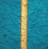
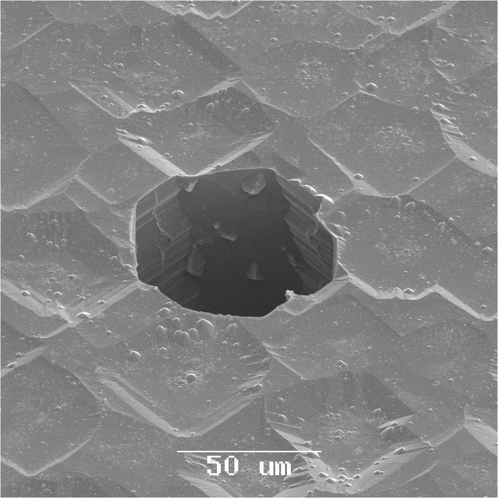
9 EXAMPLE: LASER STRUCTURING OF CIGS SOLAR MODULES Improvements in P2 structuring Gauss Top-Hat Module lay-out ZnO:Al-Layer nm ZnO-Layer nm CIGS Mo CIGS Mo P1 P2 P3 CdS-Layer~50 nm CI(G)S-Layer ~2 µm Mo-Layer ~0,5 µm µm µm Glass substrate E P = 2 µj; v f = 0,1 m/s (Multiple pass, 4x) E P = 4,4 µj; v f = 0,1 m/s (Multiple pass, 3x) Increased process window Reduced HAZ P1 P2 P3 All 3 laser patterning steps with shaped beam µm µm µm E P = 34 µj; v f = 2 m/s E P = 6,5 µj; v f = 0,1 m/s (Multiple pass, 2x) E P = 8 µj; v f = 2 m/s Experimental set-up using sub-nanosecond laser radiation at 532 nm 9
10 OUTLINE Beam Shaping for efficiency and productivity increase Efficiency increase of mc-silicon solar cell - Reflectivity reduction by laser structuring - Productivity by multiple beam structuring Roll-to-Roll Production of organic Solar modules - Practicable Laser Patterning in OPV - Laser Patterning module 10
11 OUTLINE Beam Shaping for efficiency and productivity increase Efficiency increase of mc-silicon solar cell - Reflectivity reduction by laser structuring - Productivity by multiple beam structuring Roll-to-Roll Production of organic Solar modules - Practicable Laser Patterning in OPV - Laser Patterning module 11
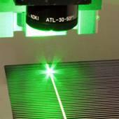
12 SETUP FOR THE FUNDAMENTAL INVESTIGATION Beam Expander Mirror Scanner f-theta objective Laser Source SHG Mirror TRUMPF TRU MICRO 5050 Average Power nm Pulse duration 7 ps Wavelength 1030 nm/515 nm Repetition rate Up to 400 khz Silicon Poly-Si Size 5 squared Isotextured 12

13 SILICON ABLATION CHARACTERISTICS 13


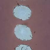
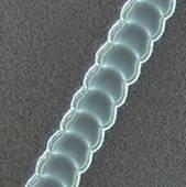
14 FORMATION OF STRUCTURES 0. untreated silicon 1. regular ripple pattern 2. pearl-like structures 3. cone-like structures Bonse 09 Sarnet 08 Nayak 11 larger energy dose I. Formation of ripples at defects II. Formation of regular ripple pattern III. Transformation to pearl-like structure IV. Transformation to cone-like structures 14


15 STRUCTURING OF SILICON Different topologies at the same laser fluence and different focal diameters Topology is mainly a function of laser fluence and number of pulses per point 15

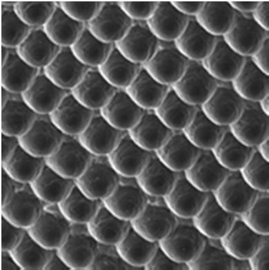
16 STRUCTURING OF SILICON Increased structure height with larger number of pulses per point Large variety of achievable topologies Schütz, V. et al. Proc. of SPIE Vol X1-7 (2012) 16


17 PROCESSING OF LARGE-SCALE SILICON WAFERS 5 isotextured Si wafer 7-spots multi-beam processing 15 minutes overall processing time Schütz, V. et al. Proc. of SPIE Vol X1-7 (2012) 17
 18")
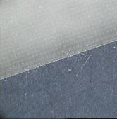
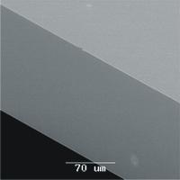
18 PROCESSING OF LARGE-SCALE SILICON WAFERS Decreased reflectivity of absolute 10% due to laser processing At certain laser parameters no dependence on crystall orientation Processing of large areas with diffractive optical element Schütz, V. et al. Proc. of SPIE Vol X1-7 (2012) 18
19 OUTLINE Beam Shaping for efficiency and productivity increase Efficiency increase of mc-silicon solar cell - Reflectivity reduction by laser structuring - Productivity by multiple beam structuring Roll-to-Roll Production of organic Solar modules - Practicable Laser Patterning in OPV - Laser Patterning module 19
20 OUTLINE Beam Shaping for efficiency and productivity increase Efficiency increase of mc-silicon solar cell - Reflectivity reduction by laser structuring - Productivity by multiple beam structuring Roll-to-Roll Production of organic Solar modules - Practicable Laser Patterning in OPV - Laser Patterning module 20


21 LASER STRUCTURING OPV CHALLENGES Goal: monolithic series connection Remove a predominantly transparent thin layer Requirement: obtaining minimal bur and minimal damage of the substrate or layer below Economically feasible for roll-to-roll mass production 21 Project PPP Nr: 13N9847


22 POLYMER SOLAR CELL AND MODULE Principles and materials PEDOT:PSS P3HT PCBM 22
23 LAY-OUT AND LASER SELECTION CRITERIA Module lay-out Transmittance of single layers GEN1: With ITO Patterning step P1 Material ITO + PEDOT:PSS Typical thicknesses [nm] Function Semi-transparent electrode P2 P3HT:PCBM 200 [nm] Photoactive-layer P3 Aluminium 200 [nm] Back contact GEN2: Without ITO Patterning step P1 P2 Material High cond. PEDOT:PSS PCDTBT: PCBM Typical thicknesses 150 [nm] Function Semi-transparent electrode 200 [nm] Photoactive-layer P3 Aluminium 200 [nm] Back contact 355 nm 532 nm 1064 nm 23

![355 Power [W] 3 0,4 Beam Quality M 2 [-] < 1.](/docs-images/75/72117774/images/24-2.jpg "25 < 1.")
24 LASER LAB SET UP Manufacturer Modell Helios GN Innolight Helios UV Wavelength [nm] Power [W] 3 0,4 Beam Quality M 2 [-] < 1.25 < 1.25 Pulse duration [ns] <0,69 < 0,69 24
25 LASER PATTERNING P1 P2 P3 50 µm 50 µm 50 µm GEN1 Laser processing P1, P2 and P3 Suitable laser sources identified Test modules in lab produced ITO ʎ = 532 nm; tp < 0,5 ns P3HT:PCBM+PEDOT:PSS ʎ = 355 nm; tp < 0,5 ns Aluminium ʎ = 532 nm; tp < 0,5 ns P1 P2 P3 50 µm 50 µm PEDOT:PSS ʎ = 532 nm; tp < 0,5 ns P3HT:PCBM ʎ = 532 nm; tp < 0,5 ns 50 µm Aluminium ʎ = 532 nm; tp < 0,5 ns GEN2 Processing alternative material systems (ITO free) All patterning steps with one laser Test modules in lab produced 25
26 TEST MODULES QUALIFICATION 50 mm x 50 mm solar modules on PET foil and glass substrate 8 cells Reached efficiencies in test modules Description sample Moduleffizienz (%) Complete laser structured module on Glas 1.51 Partially laser structured module (except for P3) on PET foil Partially laser structured module (except for P3) on PET foil with PCDTBT absorber layer ITO-free complete laser structured module on PET foil with P3HT absorber layer ELI & Lock-in Thermography of Solarmodul 26
27 ROLL-TO-ROLL PILOT MACHINE Target Cost effective mass production Process different material systems Combine different laser sources Process under different atmospheres possible Customized laser, scanner and camera system Data pilot machine Full automated laser structuring with pattern detection Band speed up to 180 m/min Maximal foil width 8 Modular coupling design P1 on 2 foil demonstrated 27
28 ROLL-TO-ROLL PILOT LASER MACHINE 28
29 REWINDER AND UNWINDER MODULES Rewinder module Band tension & position control with Cleaning unit Unwinder module 29
30 LASER STRUCTURING MODULE Front view With scanner system Rear view Laser with optics 30
31 COATING AND DRYING MODULES Dryer unit Coater unit Caoter & Dryer units 31
32 VISUAL PRESENTATIONS 2CV.6 Silicon Solar cell Improvemnts. Wednesday 26 Sept. 13:30-15:00 2CV.6.24 Black Silicon Solar Cell Processing with High Repetitive Laser Systems Presenter: Dipl.-Ing (FH) Viktor Schütz 3DV.4 Organic-based PV. Thursday 27 Sept. 17:00-18:30 3DV.4.38 Laser structuring of ITO-free organic thin-film solar modules for rollto-roll mass production Presenter: M.Sc. Javier Gonzalez 32
33 OUTLINE Beam Shaping for efficiency and productivity increase Efficiency increase of mc-silicon solar cell - Reflectivity reduction by laser structuring - Productivity by multiple beam structuring Roll-to-Roll Production of organic Solar modules - Practicable Laser Patterning in OPV - Laser Patterning module SUMMARY 33
34 SUMMARY Beam shaping: parallelize a process scaling it up Beam shaping: precisely thin film ablation without any pulse overlap Laser texturing with ultrafast lasers: reflectivity reduction for mc-si SC Laser Patterning of organic solar modules on PET without ITO R2R Pilot machine for coating, drying, laser patterning ready for use 34


35 ACKNOWLEDGEMENT The Photovoltaics Group at the LZH 35
36 THANK YOU VERY MUCH FOR YOUR ATTENTION. Laser Zentrum Hannover, Germany
37 Laser Zentrum Hannover, Germany
38 VERÖFFENTLICHUNGEN 2012: Schütz V., Horn A., Nagel H., Stute U., Black silicon solar cell processing with high repetitive laser systems, Proc. 27 th EUPVSEC 2CV.6.24, Germany, Frankfurt (2012) Schütz V., Horn A., and Stute U., High-throughput process parallelization for laser surface modification on Si-Solar cells: determination of the process window, Proc. SPIE Vol , USA, San Francisco, : Haupt O., Schütz V., and Stute U. "Multi-spot laser processing of crystalline solar cells," Proc. SPIE 7921, 79210V, doi: / , : Siegel F., Schütz V., Stute U., Kling R. Large-scale riblet surfaces using multi-spot micro machining, Proc. 29 th ICALEO, M305; Anaheim, USA, 2010 Schoonderbeek A., Schütz V., Haupt O., Stute U. Laser processing of thin films for photovoltaic applications, JLMN Vol.5, No.3, DOI: /jlmn ,

39 LAY-OUT AND MATERIALS Module lay-out Transmittance of single layers Patterning step P1 P2 Material ITO + PEDOT:PSS High cond. PEDOT:PSS P3HT:PCBM PCDTBT: PCBM Typical thicknesses [nm] 150 [nm] 200 [nm] 200 [nm] Function Semi-transparent electrode Photoactive-layer P3 Aluminium 200 [nm] Back contact 355 nm 532 nm 1064 nm 39


40 LASER STRUCTURING OPV P1 P2 P3 Laser processing P1, P2 and P3 Suitable laser sources identified Test modules in lab produced 50 µm 50 µm 50 µm ITO ʎ = 532 nm; tp < 0,5 ns P3HT:PCBM+PEDOT:PSS ʎ = 355 nm; tp < 0,5 ns Aluminium ʎ = 532 nm; tp < 0,5 ns P1 P2 P3 50 µm 50 µm 50 µm Processing alternative material systems (ITO free) All patterning steps with one laser Test modules in lab produced PEDOT:PSS ʎ = 532 nm; tp < 0,5 ns P3HT:PCBM ʎ = 532 nm; tp < 0,5 ns Aluminium ʎ = 532 nm; tp < 0,5 ns 40
 Complete laser structured module on Glas 1.")

41 TEST MODULES 50 mm x 50 mm solar modules on PET foil and glass substrate 8 cells Reached efficiencies in test modules Description sample Moduleffizienz (%) Complete laser structured module on Glas 1.51 Partially laser structured module (except for P3) on PET foil Partially laser structured module (except for P3) on PET foil with PCDTBT absorber layer ITO-free complete laser structured module on PET foil with P3HT absorber layer ELI & Lock-in Thermographie von Solarmodul 41


42 ROLL-TO-ROLL LASER PROCESSING Target Cost effective mass production Process different material systems Combine different laser sources Process under different atmospheres possible Customized laser, scanner and camera system Data pilot machine Full automated laser structuring Band speed up to 180 m/min Maximal foil width 8 Modular coupling design P1 on 2 foil demonstrated 42

43 ROLL-TO-ROLL PILOT MACHINE Rewinder and unwinder modules Laser unit Band tension and position control Coating and drying unit 43
Laser-Surface-Treatment for Photovoltaic Applications
 Available online at www.sciencedirect.com Physics Procedia 39 (2012 ) 709 716 LANE 2012 Laser-Surface-Treatment for Photovoltaic Applications Alexander Horn a,*, Cay-Christian Kalmbach a, Javier González
Picosecond Laser Patterning of ITO Thin Films
 Available online at www.sciencedirect.com Physics Procedia 12 (2011) 133 140 LiM 2011 Picosecond Laser Patterning of ITO Thin Films Anna Risch*, Ralf Hellmann University of Applied Sciences Aschaffenburg,
Investigations on repetition rate and laser wavelength for efficient generation of black silicon solar cells
 KES Transactions on Sustainable Design and Manufacturing I Sustainable Design and Manufacturing 2014 : pp.936-949 : Paper sdm14-077 Investigations on repetition rate and laser wavelength for efficient
Isolation Scribing on Hybrid Films for CIGS-Based Solar Cell Using Various Nanosecond Pulsed Laser Wavelengths
 Isolation Scribing on Hybrid Films for CIGS-Based Solar Cell Using Various Nanosecond Pulsed Laser Wavelengths Ming-Fei Chen *, Wen-Tse Hsiao **, Ming-Cheng Wang * and Ying-Fang Chen * * Department of
Laser Dicing of Silicon: Comparison of Ablation Mechanisms with a Novel Technology of Thermally Induced Stress
 Dicing of Silicon: Comparison of Ablation Mechanisms with a Novel Technology of Thermally Induced Stress Oliver HAUPT, Frank SIEGEL, Aart SCHOONDERBEEK, Lars RICHTER, Rainer KLING, Andreas OSTENDORF Zentrum
DEPTH SELECTIVE LASER SCRIBING OF THIN FILMS FOR ROLL-TO-ROLL PRODUCTION OF SILICON SOLAR CELLS Paper M902
 DEPTH SELECTIVE LASER SCRIBING OF THIN FILMS FOR ROLL-TO-ROLL PRODUCTION OF SILICON SOLAR CELLS Paper M902 Jochen Löffler, Laurie Wipliez, Martijn de Keijzer, Johan Bosman, Wim Soppe ECN, Solar Energy,
Selective Patterning of ITO on flexible PET Substrate by 1064nm picosecond Laser
 Available online at www.sciencedirect.com Physics Procedia 12 (2011) 125 132 LiM 2011 Selective Patterning of ITO on flexible PET Substrate by 1064nm picosecond Laser Shizhou Xiao*, Susana Abreu Fernandes,
PATTERNING OF OXIDE THIN FILMS BY UV-LASER ABLATION
 Journal of Optoelectronics and Advanced Materials Vol. 7, No. 3, June 2005, p. 1191-1195 Invited lecture PATTERNING OF OXIDE THIN FILMS BY UV-LASER ABLATION J. Ihlemann * Laser-Laboratorium Göttingen e.v.,
Laser Processing and Characterisation of 3D Diamond Detectors
 Laser Processing and Characterisation of 3D Diamond Detectors ADAMAS GSI meeting 3rd Dec 2015 Steven Murphy University of Manchester 3D Diamond Group / RD42 Outline Laser setup for fabricating graphitic
Laser Micromachining of Bulk Substrates and Thin Films Celine Bansal
 Laser Micromachining of Bulk Substrates and Thin Films Celine Bansal Oxford Lasers Ltd Moorbrook Park Didcot, Oxfordshire, OX11 7HP Tel: +44 (0) 1235 810088 www.oxfordlasers.com Outline Oxford Lasers Importance
Verfahrens- und Systemtechnik zum präzisen Hochleistungsabtrag mit UKP-Lasern
 Verfahrens- und Systemtechnik zum präzisen Hochleistungsabtrag mit UKP-Lasern Jens Holtkamp Motivation Ultra short pulsed lasers National Institute of Standards and Technology (NIST) Regional Laser and
DEPTH SELECTIVE LASER SCRIBING OF THIN-FILM SILICON SOLAR CELLS ON FOIL Paper M1106
 DEPTH SELECTIVE LASER SCRIBING OF THIN-FILM SILICON SOLAR CELLS ON FOIL Paper M116 Laurie Wipliez 1*, Jochen Löffler 1, Martijn de Keijzer 1, Wim Soppe 1, Thomas Sebastien 1 Aart Schoonderbeek 2, Oliver
Fabrication of the Crystalline ITO Pattern by Picosecond Laser with a Diffractive Optical Element
 Fabrication of the Crystalline ITO Pattern by Picosecond Laser with a Diffractive Optical Element C.W. Chien and C.W. Cheng* ITRI South Campus, Industrial Technology Research Institute, No. 8, Gongyan
Selective front side patterning of CZTS thin-film solar cells by picosecond laser induced material lift-off process
 Available online at www.sciencedirect.com Physics Procedia 41 (2013 ) 741 745 Lasers in Manufacturing Conference 2013 Selective front side patterning of CZTS thin-film solar cells by picosecond laser induced
R&D ACTIVITIES AT ASSCP-BHEL,GURGAON IN SOLAR PV. DST-EPSRC Workshop on Solar Energy Research
 R&D ACTIVITIES AT -BHEL,GURGAON IN SOLAR PV at the DST-EPSRC Workshop on Solar Energy Research (22 nd 23 rd April, 2009) by Dr.R.K. Bhogra, Addl. General Manager & Head Email: cpdrkb@bhel.co.in Dr.A.K.
Towards scalable fabrication of high efficiency polymer solar cells
 Towards scalable fabrication of high efficiency polymer solar cells Hui Joon Park 2*, Myung-Gyu Kang 1**, Se Hyun Ahn 3, Moon Kyu Kang 1, and L. Jay Guo 1,2,3 1 Department of Electrical Engineering and
Femtosecond Laser-induced Crystallization of Amorphous Indium Tin Oxide Film on Glass Substrate for Patterning Applications
 Femtosecond Laser-induced Crystallization of Amorphous Indium Tin Oxide Film on Glass Substrate for Patterning Applications Chung-Wei Cheng* 1, Yi-Ju Lee*, Wei-Chih Shen* 1, Jenq-Shyong Chen* and Chin-Wei
Rapid Microtooling with laser based methods
 Hochschule Mittweida University of Applied Sciences Rapid Microtooling with laser based methods R. Ebert, U. Löschner, A. Streek, J. Schille, T. Süß, L. Hartwig, U. Klötzer, H. Exner ISL 2008 Chemnitz
Micro Patterning of Crystalline Structures on a-ito Films on Plastic Substrates Using Femtosecond Laser
 Technical Communication JLMN-Journal of Laser Micro/Nanoengineering Vol. 4, No. 3, 2009 Micro Patterning of Crystalline Structures on a-ito Films on Plastic Substrates Using Femtosecond Laser Chung-Wei
Developing Enhanced Substrates for OLED SSL
 Developing Enhanced Substrates for OLED SSL DOE SSL R&D Manufacturing Workshop San Diego CA 7 May, 2014 Dr. W. Dennis Slafer MicroContinuum, Inc. 57 Smith Place Cambridge, MA 02138 www.microcontinuum.com
Vacuum Coating Process Issues for Photovoltaic Devices
 Vacuum Coating Process Issues for Photovoltaic Devices James R. Sheats Lost Arrow Consulting Palo Alto, CA sheats@lostarrowc.com * AIMCAL Fall Conference (Vacuum Web Coating), Charleston, S.C. 25 October
Manipulation and control of spatial ALD layers for flexible devices. Aimcal Memphis 2016; Edward Clerkx
 Manipulation and control of spatial ALD layers for flexible devices Meyer Burger Netherlands Equipment manufacturer Functional inkjet printing Based in Eindhoven, the Netherlands Part of world-wide Meyer
Investigations on Melting and Welding of Glass by Ultra-short Laser Radiation
 Investigations on Melting and Welding of Glass by Ultra-short Laser Radiation Alexander HORN *, Ilja MINGAREEV * and Alexander WERTH * * Lehrstuhl für Lasertechnik, Rheinisch-Westfälische Technische Hochschule
Laser-Crystallised Thin-Film Polycrystalline Silicon Solar Cells. Jonathon Dore SPREE Research Seminar - 27th June, 2013
 Laser-Crystallised Thin-Film Polycrystalline Silicon Solar Cells Jonathon Dore SPREE Research Seminar - 27th June, 2013 Contents Introduction motivation for thin-film Thin-film PV technologies Diode laser
Lasers and Laser Systems for Micro-machining
 Lasers and Laser Systems for Micro-machining Martyn Knowles Oxford Lasers Ltd Unit 8, Moorbrook Park Didcot, Oxfordshire, OX11 7HP Tel: +44 (0) 1235 810088 www.oxfordlasers.com Lasers and Laser Systems
Influence of laser marking on stainless steel surface and corrosion resistance
 Lasers in Manufacturing Conference 2015 Influence of laser marking on stainless steel surface and corrosion resistance Martin Kučera a *, Michal Švantner a, Eva Smazalová a a, New Technologies - Research
In-situ laser-induced contamination monitoring using long-distance microscopy
 In-situ laser-induced contamination monitoring using long-distance microscopy Paul Wagner a, Helmut Schröder* a, Wolfgang Riede a a German Aerospace Center (DLR), Institute of Technical Physics, Pfaffenwaldring
Lasers in Advanced Packaging
 Lasers in Advanced Packaging Xiangyang Song, Cristian Porneala, Dana Sercel, Kevin Silvia, Joshua Schoenly, Rouzbeh Sarrafi, Sean Dennigan, Eric DeGenova, Scott Tompkins, Brian Baird, Vijay Kancharla,
Laser printing and curing/sintering of silver paste lines for solar cell metallization
 Lasers in Manufacturing Conference 2015 Laser printing and curing/sintering of silver paste lines for solar cell metallization D. Munoz-Martin a *, Y. Chen a, A. Márquez a, M. Morales a, C. Molpeceres
Advantages of picosecond laser machining for cutting-edge technologies
 Available online at www.sciencedirect.com Physics Procedia 41 (2013 ) 381 388 Lasers in Manufacturing Conference 2013 Advantages of picosecond laser machining for cutting-edge technologies Abstract C.
Photovoltaics & Solar Thermals. Thin-film equipment. Customized. FHR Anlagenbau GmbH I
 Photovoltaics & Solar Thermals Thin-film equipment. Customized. FHR Anlagenbau GmbH I www.fhr.de FHR Anlagenbau GmbH is an innovative enterprise in the branch of vacuum processing and thin-film technologies.
INVESTIGATIONS ON THE THERMAL LOAD AND ACTIVE THERMAL LOAD REDUCTION DURING LASER PROCESSING OF CFRP
 21 st International Conference on Composite Materials Xi an, 20-25 th August 2017 INVESTIGATIONS ON THE THERMAL LOAD AND ACTIVE THERMAL LOAD REDUCTION DURING LASER PROCESSING OF CFRP R. Staehr 1, S. Bluemel
TFS PRODUCTION SOLUTIONS. TFS Production Solutions. For thin-film solar modules
 TFS PRODUCTION SOLUTIONS TFS Production Solutions For thin-film solar modules 2 TFS PRODUCTION SOLUTIONS MANZ AG 3 TFS PRODUCTION SOLUTIONS MANZ AG GERMAN ENGINEERING INTERNATIONALLY STAGED GLOBAL REFERENCES
Optical Inspection for the Field of Thin-Film Solar
 Top quality for the photovoltaic industry Optical Inspection for the Field of Thin-Film Solar Thin-film solar cells are playing an increasingly important role in the photovoltaic industry. Even though
ROLL TO ROLL FABRICATION PROCESS OF THIN FILM SILICON SOLAR CELLS ON STEEL FOIL
 ROLL TO ROLL FABRICATION PROCESS OF THIN FILM SILICON SOLAR CELLS ON STEEL FOIL B.B. Van Aken, M. Dörenkämper, C. Devilee, M.C.R. Heijna, J. Löffler and W.J. Soppe ECN Solar Energy, P.O. Box 1, 1755 ZG
Electroless Silver Plating as a Tool for Enhancement of Efficiency of Standard Industrial Solar Cells
 Electroless Silver Plating as a Tool for Enhancement of Efficiency of Standard Industrial Solar Cells Outline Short introduction to ISC Konstanz Plating on standard industrial solar cells Electroless Ag-plating
Optimizing the processing of sapphire with ultrashort laser pulses
 Optimizing the processing of sapphire with ultrashort laser pulses Geoff Lott 1, Nicolas Falletto 1, Pierre-Jean Devilder, and Rainer Kling 3 1 Electro Scientific Industries, Eolite Systems, 3 Alphanov
Material modification of reinforced glass fibers using pulsed laser radiation
 Lasers in Manufacturing Conference 2015 Material modification of reinforced glass fibers using pulsed laser radiation Niels Schilling a *, Benjamin Krupop a, James Bovatsek b, Scott White b, Rajesh Patel
Roll-to-roll Technology for Transparent High Barrier Films
 Roll-to-roll Technology for Transparent High Barrier Films Presented at the AIMCAL Fall Technical Conference, October 19-22, 2008, Myrtle Beach, SC, USA Nicolas Schiller, John Fahlteich, Matthias Fahland,
Production of PV cells
 Production of PV cells MWp 1400 1200 Average market growth 1981-2003: 32% 2004: 67% 1000 800 600 400 200 0 1991 1992 1993 1994 1995 1996 1997 1998 1999 2000 2001 2002 2003 2004 rest 1.0 1.0 1.0 2.0 4.0
11.3 Polishing with Laser Radiation
 196 E. Willenborg 11.3 Polishing with Laser Radiation Edgar Willenborg The surface roughness of a part or product strongly influences its properties and functions. Among these can be counted abrasion and
Challenges and Future Directions of Laser Fuse Processing in Memory Repair
 Challenges and Future Directions of Laser Fuse Processing in Memory Repair Bo Gu, * T. Coughlin, B. Maxwell, J. Griffiths, J. Lee, J. Cordingley, S. Johnson, E. Karagiannis, J. Ehrmann GSI Lumonics, Inc.
Advanced Laser scribing of thin-film solar panels. LPKF Allegro
 Advanced Laser scribing of thin-film solar panels LPKF Allegro Optimal dynamics Maximal processing speed independent of the cell orientation on the module Efficient utilization of module area Successive
KGC SCIENTIFIC TYPES OF SOLAR CELL
 KGC SCIENTIFIC www.kgcscientific.com TYPES OF SOLAR CELL How Photovoltaic Cell Work When sunshine that contain photon strike the panel, semiconductor material will ionized Causing electron to break free
Laser ablation of ITO thin films on glass for flat panel display manufacture
 Laser ablation of ITO thin films on glass for flat panel display manufacture Matt Henry, Paul M Harrison, Jozef Wendland Powerlase Ltd, Imperial House, Link 10, Napier Way, Crawley, Sussex. RH10 9RA. United
The Effects of Defects on the Moisture-Barrier Performance of Clear Coatings on Polymer Substrates.
 AIMCAL, CHARLESTON, SC, 2013 The Effects of Defects on the Moisture-Barrier Performance of Clear Coatings on Polymer Substrates. The National Centre for Printed Electronics ALF part SMITH of Centre for
Laser Cutting of Electrodes for Advanced Batteries
 Proceedings of LPM2010 - the 11th International Symposium on Laser Precision Microfabrication Laser Cutting of Electrodes for Advanced Batteries Hans J. HERFURTH, Rahul PATWA and Henrikki PANTSAR Fraunhofer
FEL Irradiation Tolerance of Multilayer Optical System
 FEL Irradiation Tolerance of Multilayer Optical System Satoshi Ichimaru, Masatoshi Hatayama NTT Advanced Technology Corporation 1. Introduction 2. Damage formation - Thermal process vs Non-thermal process
TFS PRODUCTION SOLUTIONS. TFS Production Solutions. For thin-film solar modules
 TFS PRODUCTION SOLUTIONS TFS Production Solutions For thin-film solar modules 2 TFS PRODUCTION SOLUTIONS MANZ AG 3 TFS PRODUCTION SOLUTIONS MANZ AG GERMAN ENGINEERING INTERNATIONALLY STAGED GLOBAL REFERENCES
PASHA: A NEW INDUSTRIAL PROCESS TECHNOLOGY ENABLING HIGH EFFICIENCIES ON THIN AND LARGE MC-SI WAFERS
 PASHA: A NEW INDUSTRIAL PROCESS TECHNOLOGY ENABLING HIGH EFFICIENCIES ON THIN AND LARGE MC-SI WAFERS Ingrid Romijn, Ilkay Cesar, Martien Koppes, Eric Kossen and Arthur Weeber ECN Solar Energy, P.O. Box
International Technology Roadmap for Photovoltaic (ITRPV) - 4 th Edition - Results 2012
 - 4 th Edition - Results 2012") International Technology Roadmap for Photovoltaic (ITRPV) - 4 th Edition - Results 2012 Stephan Raithel, SEMI Europe, Director PV Europe 10 July, San Francisco AGENDA Introduction of the 4 th edition of
International Technology Roadmap for Photovoltaic (ITRPV) - 4 th Edition - Results 2012 Stephan Raithel, SEMI Europe, Director PV Europe 10 July, San Francisco AGENDA Introduction of the 4 th edition of
COLLABORATIVE PROJECT
 COLLABORATIVE PROJECT Collaborative pilot project: combination of advanced laser processes for the rapid fabrication of microfluidic devices made of polymer materials Kohler/KIT TABLE OF CONTENTS 1. Introduction...
Material Needs for Thin-Film and Concentrator Photovoltaic Modules
 Material Needs for Thin-Film and Concentrator Photovoltaic Modules NREL Sarah Kurtz CDMA Conference: Opportunities for Chemicals and Materials in Wind and Solar Energy December 4, 2009 Philadelphia, PA
Nanosecond Laser Processing of Diamond Materials
 Lasers in Manufacturing Conference 2015 Nanosecond Laser Processing of Diamond Materials Jan-Patrick Hermani a, *, Christian Brecher a, Michael Emonts a a Fraunhofer IPT, Steinbachstr. 17, 52074 Aachen,
Organic Photovoltaics: A Technology Overview. Matthew Wright
 Organic Photovoltaics: A Technology Overview Matthew Wright Content Part 1: Organic Photovoltaics Overview Justification for OPV Demonstration of OPV deployment Current challenges faced Part 2: OPV research
Sputter-free and reproducible laser welding of electric or electronic copper contacts with a green laser
 Abstract Lasers in Manufacturing Conference 2015 Sputter-free and reproducible laser welding of electric or electronic copper contacts with a green laser Kaiser, Elke*; Pricking, Sebastian; Stolzenburg,
Innovative Laser Processing Technologies
 Innovative Laser Processing Technologies Reinhard Ferstl Director Sales & Marketing EMEA / Asia Corning Laser Technologies September 21, 2016 2016 Corning Incorporated Corning Market Segments and Additional
Micro processing with laser radiation
 Micro processing with laser radiation Trends and perspectives Miniaturization and highly integrated functionalization are the driving factors in the production of innovative products in almost every industrial
Supporting Information
 Copyright WILEY-VCH Verlag GmbH & Co. KGaA, 69469 Weinheim, Germany, 2013. Supporting Information for Adv. Energy Mater., DOI: 10.1002/aenm.201201027 Effect of Processing Additives on the Solidification
LOW TEMPERATURE PHOTONIC SINTERING FOR PRINTED ELECTRONICS. Dr. Saad Ahmed XENON Corporation November 19, 2015
 LOW TEMPERATURE PHOTONIC SINTERING FOR PRINTED ELECTRONICS Dr. Saad Ahmed XENON Corporation November 19, 2015 Topics Introduction to Pulsed Light Photonic sintering for Printed Electronics R&D Tools for
Laser Micromachining for Industrial Applications and R&D. 3D-Micromac AG. Symposium on Smart Integrated Systems in Chemnitz. 3D-Micromac AG
 3D-Micromac AG Symposium on Smart Integrated Systems in Chemnitz 1 1 microdice - TLS-Dicing for separation of SiC 2 microprep - for high-throughput microstructure diagnostics 3 About 3D-Micromac AG 2 microdice
Optical Coatings. Photonics 4 Luxury Coatings , Genève. Dr. Andreas Bächli Head of Optical Coatings at RhySearch, Buchs (SG)
") Optical Coatings Photonics 4 Luxury Coatings 21.06.2017, Genève Dr. Andreas Bächli Head of Optical Coatings at RhySearch, Buchs (SG) RhySearch The Research- and Innovation Center in the Rhine Valley RhySearch
Optical Coatings Photonics 4 Luxury Coatings 21.06.2017, Genève Dr. Andreas Bächli Head of Optical Coatings at RhySearch, Buchs (SG) RhySearch The Research- and Innovation Center in the Rhine Valley RhySearch
The next thin-film PV technology we will discuss today is based on CIGS.
 ET3034TUx - 5.3 - CIGS PV Technology The next thin-film PV technology we will discuss today is based on CIGS. CIGS stands for copper indium gallium selenide sulfide. The typical CIGS alloys are heterogeneous
Evaluation of Polymer Membrane Deformable Mirrors for High Peak Power Laser Machining Applications
 Evaluation of Polymer Membrane Deformable Mirrors for High Peak Power Laser Machining Applications Justin D. Mansell, Brian G. Henderson, Masataka Morita, and Gideon Robertson Active Optical Systems, LLC
Flexible functional devices at mass production level with the FLEx R2R sald platform
 Flexible functional devices at mass production level with the FLEx R2R sald platform D. Spee, W. Boonen, D. Borsa and E. Clerkx Meyer Burger (Netherlands) B.V. Meyer Burger Introduction to sald Challenges
Dr Jack Gabzdyl Product Line Manager Pulsed Lasers
 AILU PHOTONEX 08 16 th October 2008 Fiber Lasers for Medical Applications Dr Jack Gabzdyl Product Line Manager Pulsed Lasers General Advantages of Fibre Lasers Beam Quality & Stability Diffraction-limited
Laser welding of polymers
 Laser welding of polymers State of the art and innovative trends - Part I Dipl.-Ing. Andrei Boglea 1 st Internal Workshop Laser welding - a versatile process for the high performance production of polymeric
3 Pulsed laser ablation and etching of fused silica
 3 Pulsed laser ablation and etching of fused silica 17 3 Pulsed laser ablation and etching of fused silica Material erosion caused by short laser pulses takes place far from equilibrium and may be based
Roll to Roll Processing, Demonstration and Advanced Materials for Polymer Solar Cells
 Roll to Roll Processing, Demonstration and Advanced Materials for Polymer Solar Cells The Solar Energy Programme Martin Helgesen, PhD. Frederik C. Krebs, Professor Quick Status and Potential of Polymer
Water Jet Guided Laser Cutting of Silicon Thin Films Using 515nm Disk Laser
 Technical Communication JLMN-Journal of Laser Micro/Nanoengineering Vol. 6, No. 2, 11 Water Jet Guided Laser Cutting of Silicon Thin Films Using 515nm Disk Laser Eva-Maria Heilmann*, Albrecht Seidl** and
light Specific- Power CdTe Thin-Film Solar Cells using Quantum Dots Development of Highly Efficiency, Ultra-light
 Development of Highly Efficiency, Ultra-light light Weight, Radiation-Resistant, Resistant, High-Specific Specific- Power CdTe Thin-Film Solar Cells using Quantum Dots Neelkanth G. Dhere Florida Solar
ITO SPUTTER COATED FILMS FOR TOUCH PANEL APPLICATIONS USING ROTARY SINTERED CERAMIC ITO TARGETS: WHAT CAN BE LEARNED FROM GLASS COATING?
 ITO SPUTTER COATED FILMS FOR TOUCH PANEL APPLICATIONS USING ROTARY SINTERED CERAMIC ITO TARGETS: WHAT CAN BE LEARNED FROM GLASS COATING? Paul Lippens AIMCAL Web coating conference 2012 Outline Introduction
Laser treatment of gravure-printed ITO films on PET
 Laser treatment of gravure-printed ITO films on PET Howard V Snelling, Anton A Serkov, Jack Eden, Rob J Farley Physics, School of Mathematical and Physical Sciences, University of Hull, HU6 7RX, UK Presentation
PEAK EFFICIENCIES WITH FALLING MANUFACTURING COSTS
 PEAK EFFICIENCIES WITH FALLING MANUFACTURING COSTS Simple and cost-effective introduction of PERC technology into the mass production of solar cells Kerstin Strauch, Florian Schwarz, Sebastian Gatz 1 Introduction
Plasma Monitoring during Laser Material Processing
 Available online at www.sciencedirect.com Physics Procedia 12 (2011) 404 410 LiM 2011 Plasma Monitoring during Laser Material Processing David Diego-Vallejo a,b, David Ashkenasi c, *, Gerd Illing c, Hans
The Potential of Photovoltaics
 The Potential of Photovoltaics AIMCAL 2008 2008 Fall Conference Vacuum Web Coating Brent P. Nelson October 22, 2008 NREL is a national laboratory of the U.S. Department of Energy Office of Energy Efficiency
Applied Research for Vacuum Web Coating: What is Coming Next?
 Applied Research for Vacuum Web Coating: What is Coming Next? Matthias Fahland, John Fahlteich, Steffen Günther, Manuela Junghähnel, Claus Luber, Nicolas Schiller, Cindy Steiner, Steffen Straach, Michiel
Laser Processes for Micro and Nano Scale Functionalisation of Surfaces
 Laser Processes for Micro and Nano Scale Functionalisation of Surfaces Claudia Hartmann Sebastian Theiß, Fritz Klaiber, Arnold Gillner Hannover, 21.04.2010 Outline Functional structures examples from nature
TruMicro: Power meets precision. Machine tools / Power tools Laser technology / Electronics
 TruMicro: Power meets precision. Machine tools / Power tools Laser technology / Electronics Great results on a small scale. Contents Great results on a small scale. 2 Cold material processing. 4 Our expertise
Department of Applied Chemistry, School of Engineering, The University of Tokyo,
 Electronic Supplementary Material (ESI) for Journal of Materials Chemistry A. This journal is The Royal Society of Chemistry 216 Supporting Information for Interface-induced Crystallization and Nanostructure
Productivity versus Profitability in Vacuum Web Coating
 Productivity versus Profitability in Vacuum Web Coating Liz Josephson, Applied Films Corp. Longmont CO Dirk Hoffmann, Gerard Loebig Applied Films GmbH & Co. KG, Alzenau, Germany Market requirements Quality
AILU Technology Workshop
 AILU Technology Workshop Welding of metals using high power fiber delivered diode laser beams Dipl.-Ing. Mark Daichendt Laserline GmbH Mülheim-Kärlich Germany www.laserline.de 1 Outline Laserline company
Laser Micromilling :
 Laser Micromilling : An Enabling Technology for MicroComponent Replication Martyn Knowles Oxford Lasers Ltd. Unit 8, Moorbrook Park Didcot, Oxon OX11 7HP Tel: +44-1235-814433 Outline Introduction Process
Amorphous and Polycrystalline Thin-Film Transistors
 Part I Amorphous and Polycrystalline Thin-Film Transistors HYBRID AMORPHOUS AND POLYCRYSTALLINE SILICON DEVICES FOR LARGE-AREA ELECTRONICS P. Mei, J. B. Boyce, D. K. Fork, G. Anderson, J. Ho, J. Lu, Xerox
QUASI-SIMULTANEOUS LASER WELDING OF PLASTICS COMPARISON OF DIODE LASER WELDING AND FIBER LASER WELDING
 QUASI-SIMULTANEOUS LASER WELDING OF PLASTICS COMPARISON OF DIODE LASER WELDING AND FIBER LASER WELDING S. Ruotsalainen 1, P. Laakso 1 1 Lappeenranta University of Technology, Lappeenranta, Finland 2 VTT
Extensive Micro-Structuring of Metals using Picosecond Pulses Ablation Behavior and Industrial Relevance
 Extensive Micro-Structuring of Metals using icosecond ulses Ablation Behavior and Industrial Relevance rank SIEGEL *1, Ulrich KLUG *1 and Rainer KLING *1 *1 Laser Zentrum Hannover e.v., Hollerithallee
High-Rate Laser Micro Machining Systems Using Ultrashort Pulsed Lasers Uwe Wagner, 3D-Micromac AG
 High-Rate Laser Micro Machining Systems Using Ultrashort Pulsed Lasers Uwe Wagner, 3D-Micromac AG Content 1. 3D-Micromac At a glance 2. Cluster market related machine requirements 3. Solution examples
High Definition Selective Metallization for Printed Electronics
 High Definition Selective Metallization for Printed Electronics Wolfgang Decker VAST FILMS, Ltd. Outline Introduction of VAST FILMS What is Selective Metalization Range of Applications for Selective Metalization
Latest Development in Vacuum Metallisation
 Latest Development in Vacuum Metallisation Professor Nadir Ahmed Vacuum Metallising Consultant General Vacuum Equipment Ltd. Pennine Business Park, Pilsworth Road, Heywood OL10 2TL England Tel: +44(0)1706
Welding of Thin Foils with Elliptical Beams. Abe, Nobuyuki; Funada, Yoshinori; Tsukamoto, Masahiro.
 Title Author(s) Citation Welding of Thin Foils with Elliptical Beams Abe, Nobuyuki; Funada, Yoshinori; Tsukamoto, Masahiro Transactions of JWRI. 37(1) P.27-P.31 Issue Date 2008-07 Text Version publisher
Enhancement of extreme ultraviolet emission from laser irradiated targets by surface nanostructures
 Enhancement of extreme ultraviolet emission from laser irradiated targets by surface nanostructures EXTATIC WELCOME WEEK Ellie Floyd Barte, M.Sc 23 September 2017 Outline Introduction and Motivation Experiments
Laser-induced Selective Metal Plating on PP and PC/ABS Polymers Surface
 Laser-induced Selective Metal Plating on PP and PC/ABS Polymers Surface K. Ratautas 1, M. Gedvilas 1, I. Stankevičienė 1, A. Jagminienė 1, E. Norkus 1, N. Li Pira 2, S. Sinopoli 3, G. Račiukaitis 1 1 Center
Shaped Femtosecond Laser Pulse Spectroscopy for Nuclear Forensics. Phyllis Ko ANS Student Conference 2011
 Shaped Femtosecond Laser Pulse Spectroscopy for Nuclear Forensics Phyllis Ko ANS Student Conference 2011 Nuclear Forensics Analyzing nuclear material recovered from unused, intercepted devices or post-detonation
Advanced Glass Refinement by Thin Films - Trends and Challenges of Thin Film Technologies for Windows and Facade Glasses
 Advanced Glass Refinement by Thin Films - Trends and Challenges of Thin Film Technologies for Windows and Facade Glasses Dr.-Ing. Manuela Junghähnel Fraunhofer Institute for Elect ron Beam and Plasma Technology
Solar Energy Engineering
 Online Training Modules in Photovoltaics Solar Energy Engineering Starting June 2, 2014 the University of Freiburg in cooperation with Fraunhofer will be offering free special training modules in Solar
SELECTION OF OPTICAL COMPONENTS FOR COMMON LASER TYPES
 FEMTOSECOND LASER OPTICS SELECTED SPECIAL COMPONENTS METALLIC COATINGS FOR LASER AND ASTRONOMICAL APPLICATIONS 41 SELECTION OF OPTICAL COMPONENTS FOR COMMON LASER TYPES INTRODUCTION PRECISION OPTICS OPTICAL
Femtosecond Laser Materials Processing. B. C. Stuart P. S. Banks M. D. Perry
 UCRL-JC-126901 Rev 2 PREPRINT Femtosecond Laser Materials Processing B. C. Stuart P. S. Banks M. D. Perry This paper was prepared for submittal to the Manufacturing '98 Chicago, IL September 9-16, 1998
Study of Hole Properties in Percussion Regime with a New Analysis Method
 Study of Hole Properties in Percussion Regime with a New Analysis Method M. Schneider*, M. Muller*, R. Fabbro*, L. Berthe* *Laboratoire pour l Application des Lasers de Puissance (UPR CNRS 1578) 16 bis
Spatter-Free Stable Conduction and Keyhole Welding of Copper with 275 Watt Blue Laser
 Spatter-Free Stable Conduction and Keyhole Welding of Copper with 275 Watt Blue Laser Abstract Laser welding of highly reflective materials such as copper has been problematic for infrared lasers due to
Boost Your Yield Get more out of Inspection Inspection-Systems for Plastic Film and Sheets 100% Optical Web Inspection.
 Boost Your Yield Get more out of Inspection Inspection-Systems for Plastic Film and Sheets 100% Optical Web Inspection The Winning Way We deliver technology for yield management ISRA VISION: Advanced technology