Recap of a-si and a-si cell technology Types of a-si manufacturing systems a-si cell and module manufacturing at Xunlight. Xunlight Corporation
|
|
|
- Felicity Garrett
- 6 years ago
- Views:
Transcription

1 Thin-Film Silicon Technology and Manufacturing Recap of a-si and a-si cell technology Types of a-si manufacturing systems a-si cell and module manufacturing at Xunlight Xunlight products and installations Aarohi Vijh, Xunlight Corporation 3/20/2012


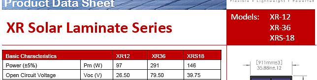
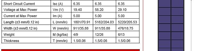
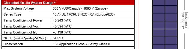
2 About Xunlight Founded in 2002; spinoff from UT Makes flexible, lightweight BIPV/BAPV modules Triple-Junction a-si Mk Makes own manufacturing equipment Plants in Toledo, OH and Kunshan, China About 80 people, 25 MW nameplate capacity
3 Recap Amorphous Silicon Inexpensive, abundant raw material End product non-toxic Strongly absorbing Low temperature coeff of power Low temperature processing possible Insensitive to water and oxygen Environmentally friendly process Substrate or superstrate configuration


4 Major Players Mitsubishi, Sharp, Kaneka Canon (until 2002), Xunlight, Unisolar Flexcell, Powerfilm, Fuji Electric Applied Materials (until last year) Oerlikon/Tokyo k Electron Dozens of small players in Asia
5 Recap Amorphous Silicon Behaves like a direct band-gap gp semiconductor Needs hydrogen for adequate electronic ect c quality Low carrier mobility (especially in doped a-si) means that p-i-n structures, rather than p-n structures must be used. Light enters through p-layer
6 Recap Amorphous Silicon Efficiency around 7% for a-si based structures Around 10% for uc-si based structures Light Induced Degradation Can be managed by using multijunction structures Can be greatly reduced by using uc-si
7 Focus of Talk Steel Substrate Roll-to-Roll Process Flexible Modules

 n-type a-si")


8 Recap Substrate-Style Style Amorphous Silicon Cell I T O TCO p-type a-si I T O intrinsic a-si or a-sige (absorber) n-type a-si Sputtered TCOs and Metal Si by Plasma Enhanced CVD (SiH4+H2+dopants) Grid deposition by thin-film or thick-film processes TCO Reflective Metal Steel
9 The i layer Function is to absorb light of specific wavelengths, and not lose too many of the photogenerated carriers Bandgap is controlled by Ge alloying Ge alloying creates more defects Bandgap grading and buffer layers are often used Microcrystalline Si is also used instead of Ge alloying.
10 The n layer Must have high optical transmission in wavelength range of interest Doped with PH3 Generally not alloyed
11 The p layer Must have high optical transmission in the absorption wavelength range of the cell it is covering. Must form good junctions with ITO and with n-layer. Two major approaches a-sic:h (using SiH4+CH4+BF3 or SiH4+TMB) a-si:h based matrix with Si crystallites, with BF3 doping.


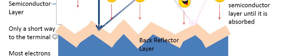

12 The Back Reflector
13 The Back-Reflector Allows thinner cells Stronger electric field, less material usage, faster deposition Usually Ag/ZnO or Al/ZnO Ag gives better NIR reflectivity but can only be used where moisture is not an issue (without special and expensive techniques) Texture/diffuse reflection is generally desirable


14 Design Consideration: Ag vs. Al in Moisture
15 The Top TCO (Window) ¼ wavelength ITO (around 70 nm)to maximize green transmission Sheet resistances sta of around ohms achievable in production
16 ITO Thickness vs. QE
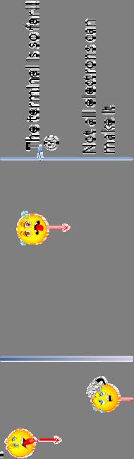
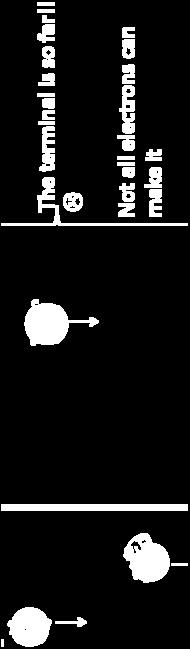
17 Recap Two-Terminal Terminal Multijunction Cell Blue Red Blue Red Vtop Contact Vbottom Vsingle = VBottom I 2I Ptandem = I * (Vbottom + Vtop) > Psingle = 2I * Vsingle because Vtop > Vbottom (and assuming contact loss is low). Current must be balanced Bandgap, thickness, reflectors are the usual knobs. Also AR. Contact/Junction loss must be low Thinner cells = stronger electric fields Many compromises in practice


18 Introduction Amorphous Silicon Triple Junction Cell Stack of 3 n-i-p cells i-layers have different Eg Lower light-induced i d degradation Voc ~ 2.2 V Jsc ~ 7-8 ma/cm 2 Stable Efficiency >11% with µc-si bottom cells (Transparent conductor) } Back Reflector Substrate Figure from: X. Deng, A. Vijh, et al., Optimization of a-sige based triple, tandem and single-junction solar cells, 31 st IEEE Photovoltaic Specialist Conference, Orlando, Florida, January, 2005.


19 IV/QE IVs: X. Deng, P. Agarwal and Q. Fan, University of Toledo
20 Types of Deposition Systems Cluster In-Line Single Piece/Batch Single Piece/Batch Roll to Roll In-Line


21 Cluster Individual chambers served by a robot Max process flexibility
22
23 In-Line Substrate moves from chamber to chamber in sequence If one chamber fails, entire e process stops


24
25 Batch Cluster Systems can be single or batch mode
26 Roll to Roll Systems
27 Characteristics of Roll-to to-roll Processing Simplicity Steady operation Well suited to high volume production Speed must be the same in all zones Time is transformed to length Pressure must generally be the same No cleanroom needed Patterning is difficult Batch sizes are large


28 Flexible a-si Manufacturing Process at Xunlight Sputter PECVD Sputter Back-Reflector Semiconductor Top TCO Cell Definition iti Passivation Contacts t & Buses Stringing Lamination Finishing
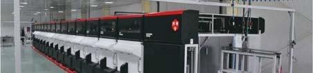
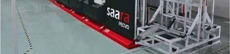
29 Xunlight 25MW PECVD/ITO Line
30 Xunlight 25MW PECVD/ITO Line 9 PECVD deposition zones (nip-nip-nip); p p p) each zone has single or multiple parallel plate electrodes, depending on deposition rates and thicknesses 1 sputter zone (ITO) Online QC capability 200 feet in length Capable of running lengths up to 8000 feet nonstop 36 wide substrate
31 Schematic of a Combined PECVD/ITO Roll to Roll Line Payout PECVD Section Differential ITO Section Online QC Takeup
32 Differential Pressure Devices 1:1000 pressure ratios achievable while allowing web to move freely, and allowing no significant cross-contamination Application number: 12/535,237 Publication number: US 2010/ A1 Filing date: Aug 4, 2009

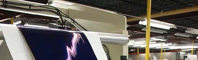
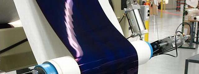

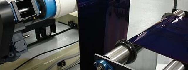

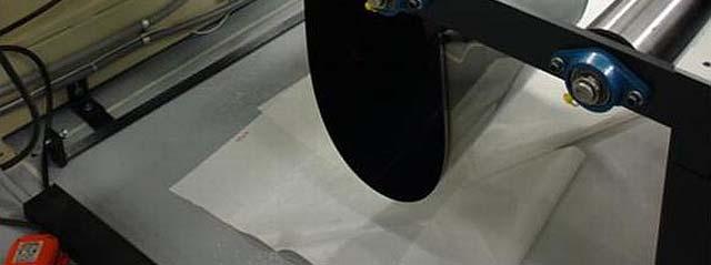

33 Photo of Coated Web
34 Back End I Singulation Edge Delete Shunt Passivation
35 Shunt Passivation Apparatus for light-assisted shunt passivation Bias Voltage V ~1-30 seconds Electrolyte, AlCl 3 Light Source Shunt Electrode Metal a-si ITO (TCO) nipnipnip Mesh Electrode Combined Light and Electrical Bias Combined Light and Electrical Bias Reduces unwanted conversion of TCO Broadens process window
36 Shunt Passivation
37 Shunt Passivation 12 Efficiency before and after shunt passivation GD AM1.5 Effi iciency (%) before after Cell #
38 Back End II Negative and Positive Buses Current Collection Grid Bypass Diodes Stringing Lamination i Testing
39 Efficiency Improvement 340 Stabilized Power (XR36 Module) Production as of early 2012 (300 W) Best Modules as of early 2012 (315 W)
40 Reliability Challenges Uncontrolled user environment Not serviceable Very long lifetime expectation with combination of sun, wind, water, high voltage, heat. Good part: No moving parts
41 Functions of Package Let light through while protecting cells from environment (Light, UV, Heat, Water, Air, Mechanical). Be stable Provide electrical insulation: 1000 V continuous use. Be resistant to fire Provide a way to mount the module Be cheap Reliability is a big part of LCOE
42 Test Sequences for Compliance UL 1703 IEC IEC and -2
43 Package Considerations Example: UV Stability EVA1 EVA1 EVA3 EVA3 EVA4 EVA4
44 References TUDelft OCW Web Site solar-cells/lectures/ Handbook of Photovoltaic Science and Engineering, g Chapter on a-si by Deng and Schiff Images: AMAT/Voith/Hind High Vacuum/Google Image Search
45 Thank You.
Amorphous Silicon Solar Cells
 The Birnie Group solar class and website were created with much-appreciated support from the NSF CRCD Program under grants 0203504 and 0509886. Continuing Support from the McLaren Endowment is also greatly
Thin film silicon technology. Cosimo Gerardi 3SUN R&D Tech. Coordinator
 Thin film silicon technology Cosimo Gerardi 3SUN R&D Tech. Coordinator 1 Outline Why thin film Si? Advantages of Si thin film Si thin film vs. other thin film Hydrogenated amorphous silicon Energy gap
Research on high efficiency and low cost thin film silicon solar cells. Xiaodan Zhang
 Research on high efficiency and low cost thin film silicon solar cells Xiaodan Zhang 2013 China-America Frontiers of Engineering, May 15-17, Beijing, China Institute Institute of of photo-electronics
Modeling of Tandem solar cell a-si/a-sige using AMPS-1D program
 Available online at www.sciencedirect.com Energy Procedia 18 (2012 ) 693 700 Modeling of Tandem solar cell a-si/a-sige using AMPS-1D program A. A. Boussettine a*, Y. Belhadji, A. Benmansour, URMER laboratory
An advantage of thin-film silicon solar cells is that they can be deposited on glass substrates and flexible substrates.
 ET3034TUx - 5.2.1 - Thin film silicon PV technology 1 Last week we have discussed the dominant PV technology in the current market, the PV technology based on c-si wafers. Now we will discuss a different
1 Introduction 1.1 Solar energy worldwide
 1 Introduction 1.1 Solar energy worldwide Solar energy, the earth s source of life, has an enormous potential to also become earth s inexhaustible and clean energy/electricity source. Each year the earth
Transparent oxides for selective contacts and passivation in heterojunction silicon solar cells
 Transparent oxides for selective contacts and passivation in heterojunction silicon solar cells Francesca Menchini Photovoltaic Technologies Laboratory, ENEA Casaccia LIMS 2018 17-18 maggio 2018 Outline
Study of a-sige:h Films and n-i-p Devices used in High Efficiency Triple Junction Solar Cells.
 Study of a-sige:h Films and n-i-p Devices used in High Efficiency Triple Junction Solar Cells. Pratima Agarwal*, H. Povolny, S. Han and X. Deng. Department of Physics and Astronomy, University of Toledo,
PV research in Neuchâtel: from high efficiency crystalline cells to novel module concepts
 PV research in Neuchâtel: from high efficiency crystalline cells to novel module concepts Laure-Emmanuelle Perret-Aebi, Christophe Ballif April 11 th 2014 Congrès Photovoltaïque National 2014, Lausanne
Production of PV cells
 Production of PV cells MWp 1400 1200 Average market growth 1981-2003: 32% 2004: 67% 1000 800 600 400 200 0 1991 1992 1993 1994 1995 1996 1997 1998 1999 2000 2001 2002 2003 2004 rest 1.0 1.0 1.0 2.0 4.0
Effects of seeding methods on the fabrication of microcrystalline silicon solar cells using radio frequency plasma enhanced chemical vapor deposition
 Thin Solid Films 483 (2005) 84 88 www.elsevier.com/locate/tsf Effects of seeding methods on the fabrication of microcrystalline silicon solar cells using radio frequency plasma enhanced chemical vapor
Amorphous silicon / crystalline silicon heterojunction solar cell
 Workshop on "Physics for Renewable Energy" October 17-29, 2005 301/1679-9 "Amorphous Silicon / Cyrstalline Silicon Heterojunction Solar Cell" E. Centurioni CNR/IMM AREA Science Park - Bologna Italy Amorphous
Triple Junction Amorphous Silicon based Flexible Photovoltaic Submodules on Polyimide Substrates
 A Dissertation entitled Triple Junction Amorphous Silicon based Flexible Photovoltaic Submodules on Polyimide Substrates by Aarohi Vijh As partial fulfillment of the requirements for the Doctor of Philosophy
Polycrystalline and microcrystalline silicon
 6 Polycrystalline and microcrystalline silicon In this chapter, the material properties of hot-wire deposited microcrystalline silicon are presented. Compared to polycrystalline silicon, microcrystalline
Thin film photovoltaics: industrial strategies for increasing the efficiency and reducing costs
 STATO E PROSPETTIVE DEL FOTOVOLTAICO IN ITALIA 26 giugno 2014 ENEA Via Giulio Romano n. 41, Roma Thin film photovoltaics: industrial strategies for increasing the efficiency and reducing costs Anna Battaglia,
Preparation and Characterization of Micro-Crystalline Hydrogenated Silicon Carbide p-layers
 Preparation and Characterization of Micro-Crystalline Hydrogenated Silicon Carbide p-layers Erten Eser, Steven S. Hegedus and Wayne A. Buchanan Institute of Energy Conversion University of Delaware, Newark,
Topics Relevant to CdTe Thin Film Solar Cells
 Topics Relevant to CdTe Thin Film Solar Cells March 13, 2012 The University of Toledo, Department of Physics and Astronomy SSARE, PVIC Principles and Varieties of Solar Energy (PHYS 4400) and Fundamentals
Introduction. 1.1 Solar energy
 1 Introduction This chapter provides a general background on solar cells. In particular, the necessity of developing thin-film silicon tandem solar cells is discussed. The working principles of two different
Solar Cell: From Research to Manufacture
 Solar Cell: From Research to Manufacture Mater. Res. Soc. Symp. Proc. Vol. 1245 2010 Materials Research Society 1245-A01-01 Thin Film Silicon Photovoltaic Technology - From Innovation to Commercialization
Two-dimensional Computer Modeling of Single Junction a-si:h Solar Cells
 Two-dimensional Computer Modeling of Single Junction a-si:h Solar Cells Changwoo Lee, Harry Efstathiadis, James E. Raynolds, Pradeep Haldar Energy and Environmental Applications Center (E2TAC) College
Low-cost, deterministic quasi-periodic photonic structures for light trapping in thin film silicon solar cells
 Low-cost, deterministic quasi-periodic photonic structures for light trapping in thin film silicon solar cells The MIT Faculty has made this article openly available. Please share how this access benefits
7 µc-si:h n-i-p solar cells on textured Ag ZnO:Al back reflectors
 7 µc-si:h n-i-p solar cells on textured Ag ZnO:Al back reflectors 7.1 Introduction The present study on ZnO:Al and textured Ag back reflectors is aimed at application in thin film µc-si n-i-p solar cells.
HANA BENEŃOVÁ 1, PETR MACH 2
 Wydawnictwo UR 2017 ISSN 2080-9069 ISSN 2450-9221 online Edukacja Technika Informatyka nr 3/21/2017 www.eti.rzeszow.pl DOI: 10.15584/eti.2017.3.11 HANA BENEŃOVÁ 1, PETR MACH 2 Suggestion for Modify of
DEVELOPMENT OF HIGH EFFICIENCY FLEXIBLE CdTe SOLAR CELLS
 DEVELOPMENT OF HIGH EFFICIENCY FLEXIBLE CdTe SOLAR CELLS A.Romeo, M. Arnold, D.L. Bätzner, H. Zogg and A.N. Tiwari* Thin Films Physics Group, Laboratory for Solid State Physics, Swiss Federal Institute
Silicon thin film e coating per il fotovoltaico
 Silicon thin film e coating per il fotovoltaico Paola Delli Veneri UTTP-Unità Tecnica Tecnologie, Laboratorio Materiali e Dispositivi di Base M.Luisa Addonizio UTTP-Unità Tecnica Tecnologie, Unità Tecnica
Amorphous and thin Si:H PV. h4p://www.motherearthnews.com/renewable Energy/Thin Film Solar UDlity Scale PV Power.aspx
 Amorphous and thin Si:H PV h4p://www.motherearthnews.com/renewable Energy/Thin Film Solar UDlity Scale PV Power.aspx Derived from LaDn silex, silicis, meaning flint. Amorphous silicon was first prepared
Solar Photovoltaic Technologies
 Solar Photovoltaic Technologies Lecture-33 Prof. C.S. Solanki Energy Systems Engineering IIT Bombay Contents Brief summary of the previous lecture Various Thin film solar cell technologies a-si CdTe, CIGS
ET3034TUx High efficiency concepts of c- Si wafer based solar cells
 ET3034TUx - 4.4 - High efficiency concepts of c- Si wafer based solar cells In the previous block we have discussed various technological aspects on crystalline silicon wafer based PV technology. In this
R&D ACTIVITIES AT ASSCP-BHEL,GURGAON IN SOLAR PV. DST-EPSRC Workshop on Solar Energy Research
 R&D ACTIVITIES AT -BHEL,GURGAON IN SOLAR PV at the DST-EPSRC Workshop on Solar Energy Research (22 nd 23 rd April, 2009) by Dr.R.K. Bhogra, Addl. General Manager & Head Email: cpdrkb@bhel.co.in Dr.A.K.
International Journal of ChemTech Research CODEN (USA): IJCRGG ISSN: Vol.9, No.01 pp , 2016
: IJCRGG ISSN: Vol.9, No.01 pp , 2016") International Journal of ChemTech Research CODEN (USA): IJCRGG ISSN: 0974-4290 Vol.9, No.01 pp 185-191, 2016 Study and Optimization Optical and Electrical properties of the p, i and n- Layers of Single
International Journal of ChemTech Research CODEN (USA): IJCRGG ISSN: 0974-4290 Vol.9, No.01 pp 185-191, 2016 Study and Optimization Optical and Electrical properties of the p, i and n- Layers of Single
ROLL TO ROLL FABRICATION PROCESS OF THIN FILM SILICON SOLAR CELLS ON STEEL FOIL
 ROLL TO ROLL FABRICATION PROCESS OF THIN FILM SILICON SOLAR CELLS ON STEEL FOIL B.B. Van Aken, M. Dörenkämper, C. Devilee, M.C.R. Heijna, J. Löffler and W.J. Soppe ECN Solar Energy, P.O. Box 1, 1755 ZG
ME 432 Fundamentals of Modern Photovoltaics. Discussion 30: Contacts 7 November 2018
 ME 432 Fundamentals of Modern Photovoltaics Discussion 30: Contacts 7 November 2018 Fundamental concepts underlying PV conversion input solar spectrum light absorption carrier excitation & thermalization
Thin film solar cells
 Thin film solar cells pn junction: a:si cells heterojunction cells: CIGS-based CdTe-based 1 Amorphous Si large concentration of defects N T >10 16 cm -3 ( dangling bonds D +, D -, D o ) passivation of
SOLAR ENERGY. Approximately 120,000 TW of solar energy strikes the earth s surface, capturing only a fraction could supply all of our energy needs.
 SOLAR ENERGY Approximately 120,000 TW of solar energy strikes the earth s surface, capturing only a fraction could supply all of our energy needs. What is Photovoltaics? Photovoltaics is a high-technology
Slide 1. Slide 2. Slide 3. Chapter 19: Electronic Materials. Learning Objectives. Introduction
 Slide 1 Chapter 19: Electronic Materials 19-1 Slide 2 Learning Objectives 1. Ohm s law and electrical conductivity 2. Band structure of solids 3. Conductivity of metals and alloys 4. Semiconductors 5.
Effects of CdCl 2 treatment on ultra-thin MOCVD-CdTe solar cells
 Effects of CdCl 2 treatment on ultra-thin MOCVD-CdTe solar cells A.J. Clayton, S. Babar, M.A. Baker, G. Kartopu, D.A. Lamb, V. Barrioz, S.J.C. Irvine Functional Thin Films, Thursday 17 th October 2013
Thin film PV Technologies Thin film Silicon PV Technology
 Thin film PV Technologies Thin film Silicon PV Technology Week 5.2 Arno Smets Thin film Silicon solar cell Semiconductor Materials IV semiconductors: Si, Ge Rn Xe Kr Ar Ne He At I Br Cl F Po Te Se S O
The Potential of Photovoltaics
 The Potential of Photovoltaics AIMCAL 2008 2008 Fall Conference Vacuum Web Coating Brent P. Nelson October 22, 2008 NREL is a national laboratory of the U.S. Department of Energy Office of Energy Efficiency
The next thin-film PV technology we will discuss today is based on CIGS.
 ET3034TUx - 5.3 - CIGS PV Technology The next thin-film PV technology we will discuss today is based on CIGS. CIGS stands for copper indium gallium selenide sulfide. The typical CIGS alloys are heterogeneous
KGC SCIENTIFIC TYPES OF SOLAR CELL
 KGC SCIENTIFIC www.kgcscientific.com TYPES OF SOLAR CELL How Photovoltaic Cell Work When sunshine that contain photon strike the panel, semiconductor material will ionized Causing electron to break free
Amorphous silicon thin film solar cells
 Amorphous silicon thin film solar cells c-si a-si large concentration of intrinsic defects N T >10 16 cm -3 ( dangling bonds D +, D -, D o ) doping more difficult, e.g. if we increase a number of free
AMORPHOUS SILICON DIOXIDE LAYER FOR HIGH EFFICIENCY CRYSTALLINE SOLAR CELLS
 International Journal of Nanotechnology and Application (IJNA) ISSN(P): 2277-4777; ISSN(E): 2278-9391 Vol. 6, Issue 5, Dec 2016, 1-6 TJPRC Pvt. Ltd. AMORPHOUS SILICON DIOXIDE LAYER FOR HIGH EFFICIENCY
Material Needs for Thin-Film and Concentrator Photovoltaic Modules
 Material Needs for Thin-Film and Concentrator Photovoltaic Modules NREL Sarah Kurtz CDMA Conference: Opportunities for Chemicals and Materials in Wind and Solar Energy December 4, 2009 Philadelphia, PA
Materials, Electronics and Renewable Energy
 Materials, Electronics and Renewable Energy Neil Greenham ncg11@cam.ac.uk Inorganic semiconductor solar cells Current-Voltage characteristic for photovoltaic semiconductor electrodes light Must specify
Laser-Crystallised Thin-Film Polycrystalline Silicon Solar Cells. Jonathon Dore SPREE Research Seminar - 27th June, 2013
 Laser-Crystallised Thin-Film Polycrystalline Silicon Solar Cells Jonathon Dore SPREE Research Seminar - 27th June, 2013 Contents Introduction motivation for thin-film Thin-film PV technologies Diode laser
Thin Film Solar Cells Fabrication, Characterization and Applications
 Thin Film Solar Cells Fabrication, Characterization and Applications Edited by Jef Poortmans and Vladimir Arkhipov IMEC, Leuven, Belgium John Wiley & Sons, Ltd Contents Series Preface Preface xiii xv 1
Crystalline Silicon Solar Cells With Two Different Metals. Toshiyuki Sameshima*, Kazuya Kogure, and Masahiko Hasumi
 Crystalline Silicon Solar Cells With Two Different Metals Toshiyuki Sameshima*, Kazuya Kogure, and Masahiko Hasumi Tokyo University of Agriculture and Technology, 2-24-16 Naka-cho, Koganei, Tokyo 184-8588,
Substrate Temperature Control of Narrow Band Gap Hydrogenated Amorphous Silicon Germanium for Solar Cells
 Asian J. Energy Environ., Vol. 5, Issue 3, (2004), pp. 211-222 Substrate Temperature Control of Narrow Band Gap Hydrogenated Amorphous Silicon Germanium for Solar Cells Mursal 1), S. Amiruddin 2), I. Usman
THIN FILM SILICON PV TECHNOLOGY
 Journal of ELECTRICAL ENGINEERING, VOL. 61, NO. 5, 2010, 271 276 THIN FILM SILICON PV TECHNOLOGY Miroslav Zeman Thin-film silicon solar cell technology is one of the promising photovoltaic technologies
Nanoscience in (Solar) Energy Research
 Energy Research") Nanoscience in (Solar) Energy Research Arie Zaban Department of Chemistry Bar-Ilan University Israel Nanoscience in energy conservation: TBP 10 TW - PV Land Area Requirements 10 TW 3 TW 10 TW Power Stations
Nanoscience in (Solar) Energy Research Arie Zaban Department of Chemistry Bar-Ilan University Israel Nanoscience in energy conservation: TBP 10 TW - PV Land Area Requirements 10 TW 3 TW 10 TW Power Stations
Sensors & Transducers 2014 by IFSA Publishing, S. L.
 Sensors & Transducers 2014 by IFSA Publishing, S. L. http://www.sensorsportal.com Investigation of Performance Silicon Heterojunction Solar Cells Using a-si: H or a-sic: H at Emitter Layer Through AMPS-1D
Fabrication of the Amorphous Silicon Thin Layers in HIT Solar Cells
 Fabrication of the Amorphous Silicon Thin Layers in HIT Solar Cells Abstract The intrinsic and n-type amorphous silicon (a-si) thin layers of the p-type substrate HIT solar cells were fabricated by plasma
PV System Components
 PV System Components PV modules each containing many PC cells. Connected in series or parallel arrays. Charge Controllers Optimally charges a storage battery for an off grid system, or Grid tie Inverters
Thin Film PV Transparent Conductive Oxide History, Functions, and Developments. Chris Cording AGC Flat Glass North America
 Thin Film PV Transparent Conductive Oxide History, Functions, and Developments Chris Cording AGC Flat Glass North America Introduction Thin-film modules often require a front Transparent Conductive Oxide
Basics of Solar Photovoltaics. Photovoltaics (PV) Lecture-21
 Lecture-21") Lecture-21 Basics of Solar Photovoltaics Photovoltaics (PV) Photovoltaics (PV) comprise the technology to convert sunlight directly into electricity. The term photo means light and voltaic, electricity.
Lecture-21 Basics of Solar Photovoltaics Photovoltaics (PV) Photovoltaics (PV) comprise the technology to convert sunlight directly into electricity. The term photo means light and voltaic, electricity.
PROMISING THIN FILMS MATERIALS FOR PHOTOVOLTAICS
 PROMISING THIN FILMS MATERIALS FOR PHOTOVOLTAICS Emmanuelle ROUVIERE CEA Grenoble (France) emmanuelle.rouviere@cea.fr Outline Introduction Photovoltaic technologies and market Applications Promising Thin
Available online at ScienceDirect. Energy Procedia 84 (2015 ) 17 24
 17 24") Available online at www.sciencedirect.com ScienceDirect Energy Procedia 84 (2015 ) 17 24 E-MRS Spring Meeting 2015 Symposium C - Advanced inorganic materials and structures for photovoltaics Annealing
Available online at www.sciencedirect.com ScienceDirect Energy Procedia 84 (2015 ) 17 24 E-MRS Spring Meeting 2015 Symposium C - Advanced inorganic materials and structures for photovoltaics Annealing
Summary and Scope for further study
 Chapter 6 Summary and Scope for further study 6.1 Summary of the present study Transparent electronics is an emerging science and technology field concentrated on fabricating invisible electronic circuits
PHYSICSOF SOLARCELLS. Jenny Nelson. Imperial College, UK. Imperial College Press ICP
 im- PHYSICSOF SOLARCELLS Jenny Nelson Imperial College, UK ICP Imperial College Press Contents Preface v Chapter 1 Introduction 1 1.1. Photons In, Electrons Out: The Photovoltaic Effect 1 1.2. Brief History
A Novel Low Temperature Self-Aligned Field Induced Drain Polycrystalline Silicon Thin Film Transistor by Using Selective Side-Etching Process
 Chapter 3 A Novel Low Temperature Self-Aligned Field Induced Drain Polycrystalline Silicon Thin Film Transistor by Using Selective Side-Etching Process 3.1 Introduction Low-temperature poly-si (LTPS) TFTs
SEMI Northeast Forum The Impact of Materials on PV Technology. Stanley Merritt Global Business Development Manager DuPont Photovoltaic Solutions
 SEMI Northeast Forum The Impact of Materials on PV Technology Stanley Merritt Global Business Development Manager DuPont Photovoltaic Solutions September 28, 2011 The Vision of DuPont To be the world s
Solar 101 for the Duke Energy Academy
 Solar 101 for the Duke Energy Academy June 23, 2014 Peter Bermel School of Electrical and Computer Engineering Outline The solar resource Approaches to harvesting solar power Solar photovoltaics technologies
"Plasma CVD passivation; Key to high efficiency silicon solar cells",
 "Plasma CVD passivation; Key to high efficiency silicon solar cells", David Tanner Date: May 7, 2015 2012 GTAT Corporation. All rights reserved. Summary: Remarkable efficiency improvements of silicon solar
Prism Solar Technologies
 1 Technologies Juan Russo, Optical Scientist Tapping Holographic Technologies to Make Photovoltaics More Cost-Effective 2 About Technologies: manufactures Holographic Planar Concentrator (HPC) film. An
Photovoltaic Fundamentals, Technology and Practice Dr. Mohamed Fawzy Aboud Sustainable Energy Technologies center (SET)
") Photovoltaic Fundamentals, Technology and Practice Dr. Mohamed Fawzy Aboud Sustainable Energy Technologies center (SET) The Greenhouse Effect 270 ppm carbon dioxide (CO 2 ) in the atmosphere absorbs outgoing
Photovoltaic Fundamentals, Technology and Practice Dr. Mohamed Fawzy Aboud Sustainable Energy Technologies center (SET) The Greenhouse Effect 270 ppm carbon dioxide (CO 2 ) in the atmosphere absorbs outgoing
PHOTOVOLTAIC CELLS
 www.ljuhv.com PHOTOVOLTAIC CELLS How Photovoltaic Cell Work When sunshine that contain photon strike the panel, semiconductor material will ionized Causing electron to break free from their bond. Due to
DEPTH SELECTIVE LASER SCRIBING OF THIN FILMS FOR ROLL-TO-ROLL PRODUCTION OF SILICON SOLAR CELLS Paper M902
 DEPTH SELECTIVE LASER SCRIBING OF THIN FILMS FOR ROLL-TO-ROLL PRODUCTION OF SILICON SOLAR CELLS Paper M902 Jochen Löffler, Laurie Wipliez, Martijn de Keijzer, Johan Bosman, Wim Soppe ECN, Solar Energy,
Technologie Evolutives et Disruptives pour les prochaines générations de cellules solaires Silicium
 Technologie Evolutives et Disruptives pour les prochaines générations de cellules solaires Silicium M. Despeisse, on behalf of CSEM and EPFL/pvlab research teams pictures 6 cm high at 11 cm vertical Swiss
pure excellence. pure energy.
 pure excellence. pure energy. The heart of a high-quality photovoltaic system is a high class photovoltaic module. The Austrian technology company Energetica produces photovoltaic modules, which are characterized
Microwave PECVD of Micro-Crystalline Silicon
 Microwave PECVD of Micro-Crystalline Silicon Wim Soppe 1, Camile Devilee 1, Sacha Schiermeier 1, Harry Donker 2, J.K. Rath 3 1 ECN Solar Energy, P.O. Box 1, 1755 ZG Petten, The Netherlands. 2 Laboratory
AQUEOUS CRITICAL CLEANING: A WHITE PAPER THE SIGNIFICANCE IN SOLAR MODULE MANUFACTURING
 AQUEOUS CRITICAL CLEANING: A WHITE PAPER THE SIGNIFICANCE IN SOLAR MODULE MANUFACTURING Alconox, Inc. Critical Cleaning Experts 30 Glenn St., Suite 309, White Plains NY 10603 USA Tel.914.948.4040 Fax.914.948.4088
Hot-wire deposited intrinsic amorphous silicon
 3 Hot-wire deposited intrinsic amorphous silicon With the use of tantalum as filament material, it is possible to decrease the substrate temperature of hot-wire deposited intrinsic amorphous silicon, while
Available online at
 Available online at www.sciencedirect.com Journal of Non-Crystalline Solids 354 (2008) 2397 2402 www.elsevier.com/locate/jnoncrysol Fabrication and optimization of single-junction nc-si:h n i p solar cells
An Efficient Silicon (Oxide) Based n/n+/p Distributed Bragg Intermediate Reflector For Multi- Junction Solar Cells
 Based n/n+/p Distributed Bragg Intermediate Reflector For Multi- Junction Solar Cells") An Efficient Silicon (Oxide) Based n/n+/p Distributed Bragg Intermediate Reflector For Multi- Junction Solar Cells Simon Kirner 1, Andre Hoffmann 2, Max Klingsporn 1, Patrick Krüger 1, Karsten Bittkau
An Efficient Silicon (Oxide) Based n/n+/p Distributed Bragg Intermediate Reflector For Multi- Junction Solar Cells Simon Kirner 1, Andre Hoffmann 2, Max Klingsporn 1, Patrick Krüger 1, Karsten Bittkau
Roll to Roll Flexible Microgroove Based Photovoltaics. John Topping Chief Scientist Big Solar Limited
 Roll to Roll Flexible Microgroove Based Photovoltaics John Topping Chief Scientist Big Solar Limited Big Solar Limited, Washington Business Centre 2 Turbine Way, Sunderland SR5 3NZ Email: John@powerroll.solar
Transmission Mode Photocathodes Covering the Spectral Range
 Transmission Mode Photocathodes Covering the Spectral Range 6/19/2002 New Developments in Photodetection 3 rd Beaune Conference June 17-21, 2002 Arlynn Smith, Keith Passmore, Roger Sillmon, Rudy Benz ITT
G.Pucker, Y.Jestin Advanced Photonics and Photovoltaics Group, Bruno Kessler Foundation, Via Sommarive 18, Povo (Trento) Italy
 Italy") F. Sgrignuoli, P. Ingenhoven, A. Anopchenko, A.Tengattini, D.Gandolfi, L. Pavesi Nanoscience Laboratory, Department of Physics, University of Trento,Via Sommarive 14, 38123 Povo (Trento) Italy. G.Pucker,
F. Sgrignuoli, P. Ingenhoven, A. Anopchenko, A.Tengattini, D.Gandolfi, L. Pavesi Nanoscience Laboratory, Department of Physics, University of Trento,Via Sommarive 14, 38123 Povo (Trento) Italy. G.Pucker,
Light-Induced Degradation of Thin Film Silicon Solar Cells
 Journal of Physics: Conference Series PAPER OPEN ACCESS Light-Induced Degradation of Thin Film Silicon Solar Cells To cite this article: F U Hamelmann et al 2016 J. Phys.: Conf. Ser. 682 012002 View the
DESIGN AND OPERATING PRINCIPLES OF III- V SOLAR CELLS
 DESIGN AND OPERATING PRINCIPLES OF III- V SOLAR CELLS ANTHONY MELECO CAPSTONE ADVISER: DR. IAN SELLERS TABLE OF CONTENTS Abstract... 3 Introduction... 3 Procedure... 4 Photomask... 4 Modeling... 5 IV curve...
PEAK EFFICIENCIES WITH FALLING MANUFACTURING COSTS
 PEAK EFFICIENCIES WITH FALLING MANUFACTURING COSTS Simple and cost-effective introduction of PERC technology into the mass production of solar cells Kerstin Strauch, Florian Schwarz, Sebastian Gatz 1 Introduction
Photovoltaics under concentrated sunlight
 Photovoltaics under concentrated sunlight April 2, 2013 The University of Toledo, Department of Physics and Astronomy Principles and Varieties of Solar Energy (PHYS 4400) Reading assignment: Sections 9.4
Vacuum Coating Process Issues for Photovoltaic Devices
 Vacuum Coating Process Issues for Photovoltaic Devices James R. Sheats Lost Arrow Consulting Palo Alto, CA sheats@lostarrowc.com * AIMCAL Fall Conference (Vacuum Web Coating), Charleston, S.C. 25 October
TEMPERATURE TESTING AND ANALYSIS OF PV MODULES PER ANSI/UL 1703 AND IEC STANDARDS
 TEMPERATURE TESTING AND ANALYSIS OF PV MODULES PER ANSI/UL 1703 AND IEC 61730 STANDARDS Jaewon Oh 1 and GovindaSamy TamizhMani 1,2 1 Arizona State University, Mesa, AZ, United States 2 TÜV Rheinland PTL,
Durable Neutral Color Anti-Reflective Coating for Mobile Displays
 Durable Neutral Color Anti-Reflective Coating for Mobile Displays By John Madocks and Phong Ngo, General Plasma, Inc. Figure 1: Samsung S4 with top half of cover glass coated with AR+DLC Abstract An in-line
New Performance Levels for TPV Front Surface Filters
 LM-4K54 June 1, 24 New Performance Levels for TPV Front Surface Filters TD Rahmlow, JE Lazo-Wasem, EJ Gratrix, PM Fourspring, and DM DePoy NOTICE This report was prepared as an account of work sponsored
Photoelectroche mical Hydrogen Production
 Photoelectroche mical Hydrogen Production DE- FC36-00GO10538 Final Report Reporting Period: 05/01/2000 06/30/2004 Hawaii Natural Energy Institute University of Hawaii at Manoa 1680 East- West Road, POST
Advanced Glass Refinement by Thin Films - Trends and Challenges of Thin Film Technologies for Windows and Facade Glasses
 Advanced Glass Refinement by Thin Films - Trends and Challenges of Thin Film Technologies for Windows and Facade Glasses Dr.-Ing. Manuela Junghähnel Fraunhofer Institute for Elect ron Beam and Plasma Technology
AIMCAL Fall Technical Conference & 19th International Conference on Vacuum Web Coating
 AIMCAL Fall Technical Conference & 19th International Conference on Vacuum Web Coating A.G. Talma, R. Schlatmann, J.W.G. Mahy Akzo Nobel Chemicals bv, P.O. Box 9300, 6800 SB Arnhem, The Netherlands. Phone
Amorphous Silicon Based Solar Cells
 Syracuse University SURFACE Physics College of Arts and Sciences 2003 Amorphous Silicon Based Solar Cells Xunming Deng University of Toledo Eric A. Schiff Syracuse University Follow this and additional
Ultra High Barrier Coatings by PECVD
 Society of Vacuum Coaters 2014 Technical Conference Presentation Ultra High Barrier Coatings by PECVD John Madocks & Phong Ngo, General Plasma Inc., 546 E. 25 th Street, Tucson, Arizona, USA Abstract Silicon
Low-temperature fabrication of dye-sensitized solar cells by transfer. of composite porous layers supplementary material
 Low-temperature fabrication of dye-sensitized solar cells by transfer of composite porous layers supplementary material Michael Dürr, Andreas Schmid, Markus Obermaier, Silvia Rosselli, Akio Yasuda, and
Performance Improvements in PV Modules Using Ionomer Encapsulants
 Performance Improvements in PV Modules Using Ionomer Encapsulants Mark Jacobson Sr. Accounts Manager, DuPont Encapsulants Cleveland, OH April 9, 2011 2 Agenda Encapsulant requirements Failure modes Moisture
Fundamentals of photovoltaic energy conversion and conventional solar cells. A.Martí September 2018, MATENER ICMAB, Campus UAB, Barcelona
 Fundamentals of photovoltaic energy conversion and conventional solar cells A.Martí 17-20 September 2018, MATENER 2018 ICMAB, Campus UAB, Barcelona Outline Fundamentals of photovoltaic energy conversion
REAR SURFACE PASSIVATION OF INTERDIGITATED BACK CONTACT SILICON HETEROJUNCTION SOLAR CELL AND 2D SIMULATION STUDY
 REAR SURFACE PASSIVATION OF INTERDIGITATED BACK CONTACT SILICON HETEROJUNCTION SOLAR CELL AND 2D SIMULATION STUDY Meijun Lu 1,2, Ujjwal Das 1, Stuart Bowden 1, and Robert Birkmire 1,2 1 Institute of Energy
Hydrogenated Amorphous Silicon Nitride Thin Film as ARC for Solar Cell Applications
 ISSN 2278 211 (Online) Hydrogenated Amorphous Silicon Nitride Thin Film as ARC for Solar Cell Applications Dr. G. Natarajan Professor & Head, Department of Physics PSNA College of Engineering and Technology,
A Novel Buried-Emitter Photovoltaic Cell for High Efficiency Energy Conversion
 A Novel Buried-Emitter Photovoltaic Cell for High Efficiency Energy Conversion by Roohollah Samadzadeh Tarighat A thesis presented to the University of Waterloo in fulfillment of the thesis requirement
Solar Cells. Mike McGehee Materials Science and Engineering
 Solar Cells Mike McGehee Materials Science and Engineering Why solar cells are likely to provide a significant fraction of our power We need ~ 30 TW of power, the sun gives us 120,000 TW. Solar cells are
Semiconductor Device Fabrication
 5 May 2003 Review Homework 6 Semiconductor Device Fabrication William Shockley, 1945 The network before the internet Bell Labs established a group to develop a semiconductor replacement for the vacuum
Material and solar cell research in high efficiency micromorph tandem solar cell
 434 Artigo original DOI: http://dx.doi.org/105902/2179460x Ciência enatura, Santa Maria, v. 37 Part 2 2015, p. 434-440 Revista do Centro de Ciências Naturais e Exatas UFSM ISSN impressa: 0100-8307 ISSN
Polycrystalline CdS/CdTe solar cells
 Polycrystalline CdS/CdTe solar cells Al Compaan Distinguished University Professor of Physics, Emeritus (Lecture for Heben/Ellingson solar cells class) March 3, 2011 1 Absorption spectra of various semiconductors